

Page 1
LTC1472
FEATURES
■
Both VCC and VPP Switching in a Single Package
■
Built-In Current Limit and Thermal Shutdown
■
16-Pin (Narrow) SOIC Package
■
Inrush Current Limited (Drives 150µF Loads)
■
Continuous 12V Power Not Required
■
Extremely Low R
■
Guaranteed 1A VCC Current and 120mA VPP Current
■
1µA Quiescent Current in Standby
■
No External Components Required
■
Compatible with Industry Standard Controllers
■
Break-Before-Make Switching
■
Controlled Rise and Fall Times
NMOS Switches
DS(ON)
U
APPLICATIONS
■
Notebook Computers
■
Palmtop Computers
■
Pen-Based Computers
■
Handi-Terminals
■
Bar-Code Readers
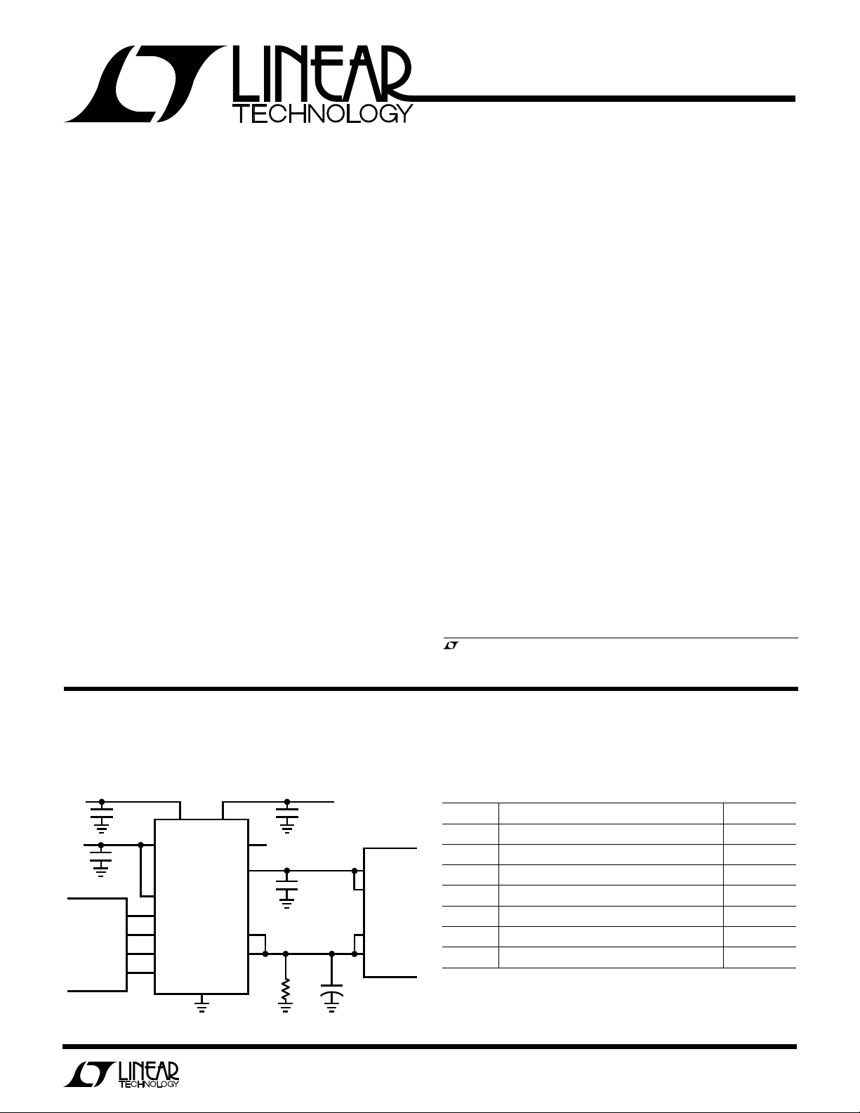
Protected PCMCIA V
CC
and
VPP Switching Matrix
U
DESCRIPTION
The LTC®1472 switching matrix routes power to both the
VCC and VPP power supply pins of the PCMCIA compatible
card socket. The V
between three operating states: OFF, 3.3V, and 5V. The
VPP output is switched between four operating states: 0V,
VCC, 12V, and Hi-Z. The output voltages are selected by
two sets of digital inputs which are compatible with
industry standard PC Card controllers (see Truth Tables).
The VCC output of the LTC1472 can supply up to 1A of
current and the VPP output up to 120mA. Both switches
have built-in SafeSlotTM current limiting and thermal shutdown to protect the card, socket and power supply against
accidental short-circuit conditions.
The LTC1472 is designed to conserve power by automatically dropping to 1µA standby current when the two
outputs are switched OFF. A shutdown pin is provided
which holds the external 12V regulator in standby mode
except when required for VPP power.
The LTC1472 is available in 16-pin SO.
, LTC and LT are registered trademarks of Linear Technology Corporation.
SafeSlot is a trademark of Linear Technology Corporation.
output of the LTC1472 is switched
CC
TYPICAL APPLICATION
Protected PCMCIA VCC and VPP Card Driver
3.3V
5V
CARD SLOT
CONTROLLER
PCMCIA
0.1µF
0.1µF
3V
IN
5V
IN
LTC1472
V
DD
VPP EN0
VPP EN1
V
EN0
CC
V
EN1
CC
GND
VPP
SHDN
VPP
V
CC(IN)
V
CC(OUT)
IN
TO 12V REGULATOR
OV, V
OUT
U
0.1µF
, 12V, Hi-Z
CC
0.1µF
OFF, 3.3V, 5V
+
10k
12V
1µF
VPP1
VPP2
PCMCIA
CARD SLOT
V
CC
V
CC
LTC1472-TA01
Linear Technology PCMCIA Product Family
DEVICE DESCRIPTION PACKAGE
LT®1312 Single PCMCIA VPP Driver/Regulator 8-Pin SO
LT1313 Dual PCMCIA VPP Driver/Regulator 16-Pin SO*
LTC1314 Single PCMCIA Switch Matrix 14-Pin SO
LTC1315 Dual PCMCIA Switch Matrix 24-Pin SSOP
LTC1470 Protected VCC 5V/3.3V Switch Matrix 8-Pin SO
LTC1471 Dual Protected VCC 5V/3.3V Switch Matrix 16-Pin SO*
LTC1472 Protected VCC and VPP Switch Matrix 16-Pin SO*
*Narrow Body
1
Page 2
LTC1472
TOP VIEW
S PACKAGE
16-LEAD PLASTIC SO
T
JMAX
= 100°C, θJA = 100°C/W
1
2
3
4
5
6
7
8
16
15
14
13
12
11
10
9
V
CC(OUT)
5V
IN
V
CC
EN1
V
CC
EN0
VPP
IN
SHDN
VPP EN0
VPP EN1
V
CC(OUT)
3V
IN
3VIN
GND
V
CC(IN)
VPP
OUT
GND
V
DD
WW
W
ABSOLUTE MAXIMUM RATINGS
U
PACKAGE/ORDER INFORMATION
5VIN Supply Voltage ................................... – 0.3V to 7V
3VIN Supply Voltage ................................... –0.3V to 7V
VPPIN Supply Voltage ............................ –0.3V to 13.2V
V
V
VPP
V
Supply Voltage...................................–0.3 to 7V
CC(IN)
Supply Voltage ............................... –0.3V to 7V
DD(IN)
(OFF) ........................................ –0.3V to 13.2V
OUT
CC(OUT)
(OFF) ............................................ –0.3V to 7V
Enable Inputs.............................................. –0.3V to 7V
VPP
V
Short-Circuit Duration ........................ Indefinite
OUT
CC(OUT)
Short-Circuit Duration ....................... Indefinite
Operating Temperature Range ..................... 0°C to 70°C
Junction Temperature...........................................100°C
Storage Temperature Range ................. –65°C to 150°C
Lead Temperature (Soldering, 10 sec).................. 300°C
ELECTRICAL CHARACTERISTICS
5VIN = 5V, 3VIN = 3.3V, VPP EN0 = VPP EN1 = OV, TA = 25°C, (Note 1) unless otherwise noted.
(VCC Switch Section)
Consult factory for Industrial and Military grade parts.
U
ORDER PART
NUMBER
LTC1472CS
W
U
SYMBOL PARAMETER CONDITIONS MIN TYP MAX UNITS
5V
IN
3V
IN
I
5VIN
I
3VIN
R
ON
I
LKG
I
LIM5V
I
LIM3V
V
CCENH
V
CCENL
I
VCCEN
t
VCC1
t
VCC2
t
VCC3
2
5VIN Supply Voltage Range (Note 2) 4.75 5.25 V
3VIN Supply Voltage Range (Note 3) 0 3.60 V
5VIN Supply Current Program to Hi-Z ● 0.01 10 µA
Program to 5V, No Load
Program to 3.3V, No Load
3VIN Supply Current Program to Hi-Z. ● 0.01 10 µA
Program to 5V, No Load
Program to 3.3V, No Load
5V Switch On Resistance Program to 5V, I
3.3V Switch On Resistance Program to 3.3V, I
Output Leakage Current OFF V
V
5V Current Limit Program to 5V, V
CC(OUT)
V
3.3V Current Limit Program to 3.3V, V
CC(OUT)
VCC Enable Input High Voltage ● 2V
V
Enable Input Low Voltage ● 0.8 V
CC
V
Enable Input Current 0V ≤ V
CC
Delay + Rise Time From 0V to 3.3V, R
Delay + Rise Time From 3.3V to 5V, R
Delay + Rise Time From 0V to 5V, R
EN0 = V
CC
CCEN
= 500mA 0.14 0.18 Ω
OUT
= 500mA 0.12 0.16 Ω
OUT
EN1 = 0V or 5V, 0V ≤ V
CC
= 0V (Note 4) 1 A
CC(OUT)
= 0V (Note 4) 1 A
CC(OUT)
≤ 5V ● ±1 µA
= 100Ω, C
LOAD
LOAD
LOAD
= 100Ω, C
= 100Ω, C
LOAD
LOAD
LOAD
≤ 5V ● ±10 µA
CC(OUT)
= 1µF (Note 5) 0.2 0.32 1 ms
= 1µF (Note 5) 0.2 0.52 1 ms
= 1µF (Note 5) 0.2 0.38 1 ms
● 140 200 µA
● 100 160 µA
● 0.01 10 µA
● 40 80 µA
Page 3
LTC1472
ELECTRICAL CHARACTERISTICS
VDD = 5V, V
= 5V, VPPIN = 12V, V
CC(IN)
CCEN0
= V
CCEN1
(VPP Switch Section)
= 0V, TA= 25°C, (Note 1), unless otherwise noted.
SYMBOL PARAMETER CONDITIONS MIN TYP MAX UNITS
V
CC(IN)
VPP
V
DD
I
CCIN
I
PPIN
I
DD
I
VPPOUT
R
ON
VPP
VPP
I
VPPEN
V
SDH
V
SDL
I
LIMVCC
I
LIMVPP
t
VPP1
t
VPP2
t
VPP3
t
VPP4
t
VPP5
t
VPP6
t
VPP7
t
VPP8
IN
ENH
ENL
VCC Input Voltage Range ● 3 5.5 V
VPP Input Voltage Range (Note 6) ● 0 12.6 V
Logic Supply Voltage Range (Note 7) ● 4.5 5.5 V
V
Supply Current, No Load Program to VPPIN or V
CC(IN)
Program to 0V or Hi-Z
VPPIN Supply Current, No Load Program to VPPIN or V
Program to 0V or Hi-Z
VDD Supply Current, No Load Program to VPP
Program to V
Program to V
IN
, VPPIN = 0V ● 85 150 µA
CC(IN)
, VPPIN = 12V ● 40 80 µA
CC(IN)
Program to 0V or Hi-Z
Hi-Z Output Leakage Current Program to Hi-Z, 0V < VPP
On Resistance VPP
On Resistance VPP
On Resistance VPP
to VPP
OUT
OUT
OUT
IN
to V
CC(IN)
to GND VDD = 5V, I
VPPIN = 12V, I
V
CC(IN)
= 120mA 0.50 1 Ω
LOAD
= 5V, I
= 5mA 1.70 5 Ω
LOAD
= 1mA 100 250 Ω
SINK
VPPIN = 12V ● 35 60 µA
CC(IN)
CC(IN)
< 12V ● 0.01 10 µA
OUT
● 0.01 10 µA
● 40 80 µA
● 0.01 10 µA
● 70 120 µA
● 0.01 10 µA
VPP Enable Input High Voltage VDD = 5V ● 2V
VPP Enable Input Low Voltage VDD = 5V ● 0.8 V
VPP Enable Input Current 0V < VPP EN < VDD ● ±1 µA
SHDN Output High Voltage Program to 0V, V
SHDN Output Low Voltage Program to VPPIN, I
VPP
Current Limit, V
OUT
VPP
Current Limit, VPP
OUT
CC(IN)
IN
Delay and Rise Time From 0V to V
Program to V
CC(IN)
Program to VPPIN, VPP
CC(IN)
or Hi-Z, I
CC(IN)
= 400µA ● 0.4 V
SINK
, VPP
= 0V (Note 4) 60 mA
OUT
= 0V (Note 4) 100 mA
OUT
= 400µA ● 3.5 V
LOAD
,VPPIN = 0V (Note 8) 5 15 50 µs
Delay and Rise Time From 0V to VPPIN (Note 8) 25 85 250 µs
Delay and Rise Time From V
Delay and Fall Time From VPPIN to V
to VPPIN (Note 8) 30 100 300 µs
CC(IN)
(Note 9) 5 15 50 µs
CC(IN)
Delay and Fall Time From VPPIN to 0V (Note 10) 10 35 100 µs
Delay and Fall Time From V
Output Turn-On Delay From Hi-Z to V
to 0V, VPPIN = 0V (Note 10) 10 30 100 µs
CC(IN)
(Note 8) 5 15 50 µs
CC(IN)
Output Turn-On Delay From Hi-Z to VPPIN (Note 8) 25 85 250 µs
The ● denotes the specifications which apply over the full operating
temperature range.
Note 1: V
ENH
= 5V, V
= 0V. See VCC and VPP Switch Truth Tables for
ENL
programming enable inputs for desired output states.
Note 2: Power for the V
from the 5V
power supply which must be continuously powered. 12V
IN
and 3.3V power is not required to control the NMOS V
input logic and charge pump circuitry is derived
CC
switches. (See
CC
Applications Information.)
Note 3: The two 3V
together and the two V
together. The 3V
supply input pins (14 and 15) must be connected
IN
supply pins do not need to be continuously powered
IN
output pins (1 and 16) must be connected
CC(OUT)
and may drop to 0V when not required.
Note 4: The V
and VPP output are protected with foldback current limit
CC
which reduces the short-circuit (0V) currents below peak permissible
current levels at higher output voltages.
Note 5: To 90% of final value.
Note 6: 12V power is only required when VPP
is programmed to 12V.
OUT
The external 12V regulator can be shutdown at all other times. Built-in
charge pumps power the internal NMOS switches from the 5V V
supply
DD
when 12V is not present.
Note 7: Power for the VPP input logic and charge pump circuitry is derived
from the V
Note 8: To 90% of the final value, C
Note 9: To 10% of the final value, C
Note 10: To 50% of the initial value, C
power supply which must be continuously powered.
DD
= 0.1µF, R
OUT
= 0.1µF, R
OUT
OUT
= 0.1µF, R
OUT
OUT
= 2.9k.
= 2.9k.
= 2.9k.
OUT
3
Page 4
LTC1472
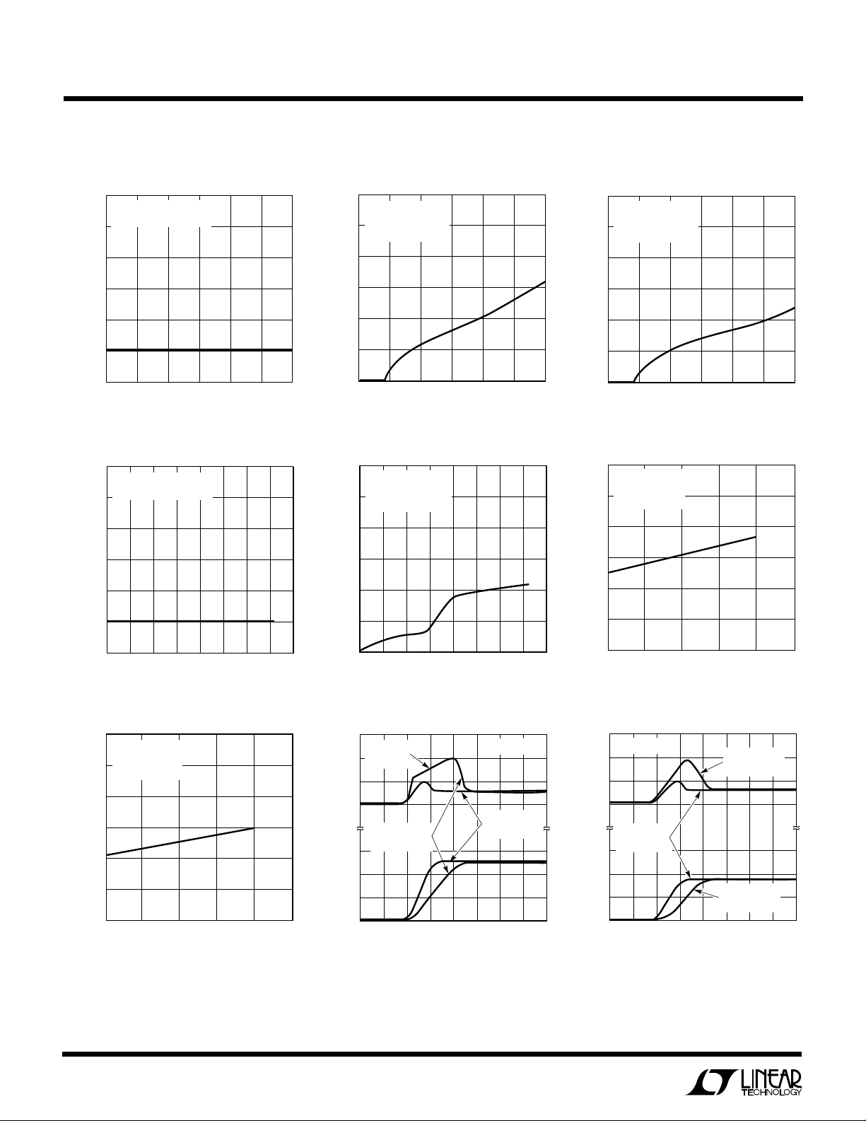
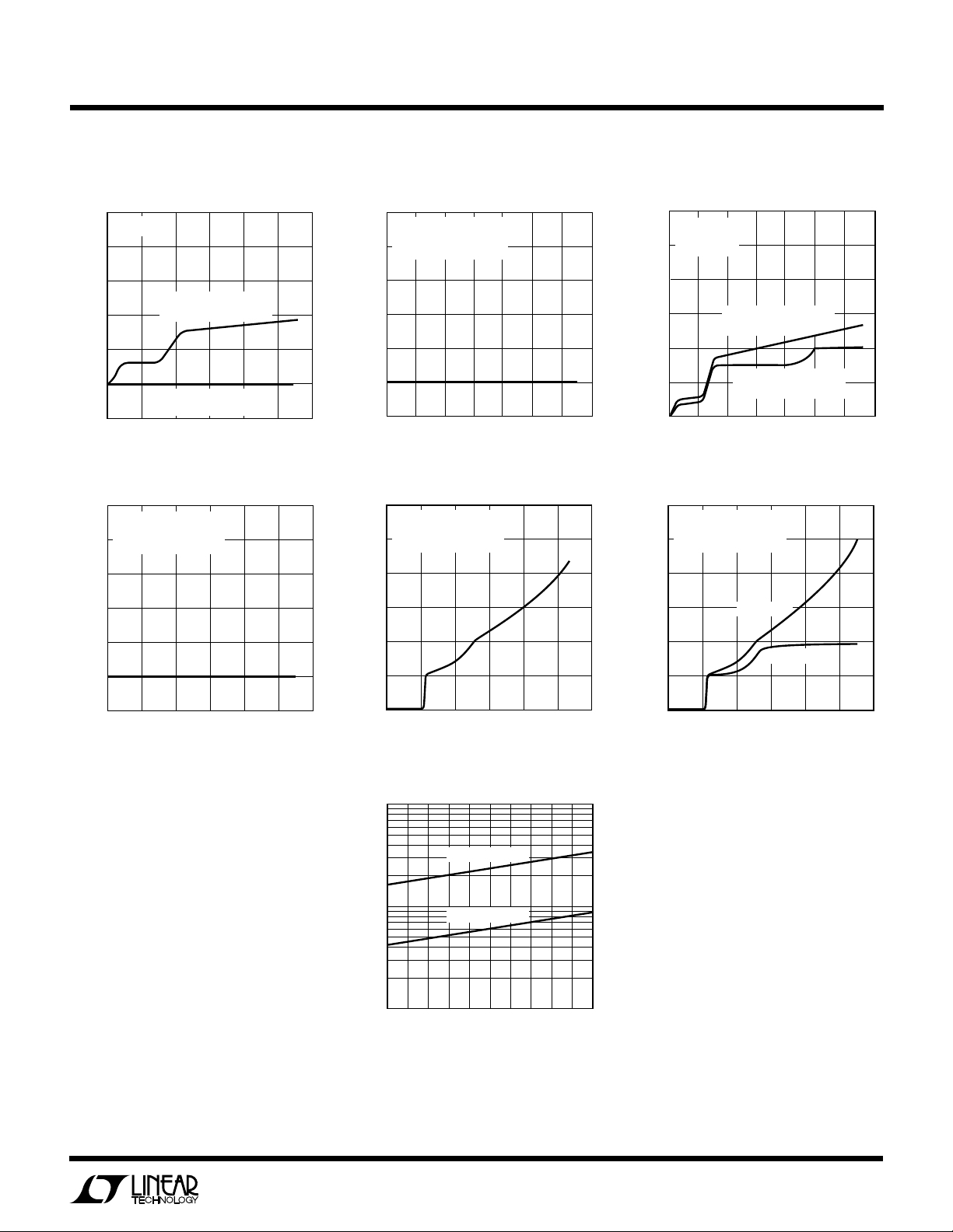
TIME (ms)
–0.2
INRUSH CURRENT (A)OUTPUT VOLTAGE (V)
0
1
1.4
LTC1472 TPC09
6
4
0
0.2
0.6
1.0
2
3
2
0
0.4
0.8
1.2
C
OUT
= 150µF
R
OUT
= 6.6Ω
C
OUT
= 150µF
R
OUT
= 6.6Ω
C
OUT
= 15µF
R
OUT
= 6.6Ω
TJ = 25°C
5VIN SUPPLY VOLTAGE (V)
0
0
5V
IN
SUPPLY CURRENT (µA)
50
100
150
200
300
1
234
LTC1472 TPC03
56
250
TA = 25°C V
CC(OUT)
PROGRAMMED
TO 3.3V, NO LOAD
W
U
TYPICAL PERFORMANCE CHARACTERISTICS
(VCC Section) VPP EN0 = VPP EN1 = 0V
5VIN Supply Current (OFF)
5
TA = 25°C V
PROGRAMMED TO OFF
4
3
2
1
SUPPLY CURRENT (µA)
IN
5V
0
–1
0
5
T
PROGRAMMED TO OFF
4
3
2
CC(OUT)
234
1
5VIN SUPPLY VOLTAGE (V)
= 25°C OUTPUT
A
5VIN Supply Current (5V ON) 5VIN Supply Current (3.3V ON)
56
LTC1472 TPC01
300
250
200
150
100
SUPPLY CURRENT (µA)
IN
5V
50
0
TA = 25°C V
PROGRAMMED
TO 5V, NO LOAD
0
1
5VIN SUPPLY VOLTAGE (V)
CC(OUT)
234
56
LTC1472 TPC02
5V Switch Resistance3VIN Supply Current (3.3V ON)3VIN Supply Current (OFF)
120
T
PROGRAMMED TO
100
3.3V, NO LOAD
80
60
= 25°C V
A
CC(OUT)
0.30
0.25
0.20
0.15
V
CC(OUT)
PROGRAMMED
TO 5V
SUPPLY CURRENT (µA)
3V
3.3V SWITCH RESISTANCE (Ω)
4
1
IN
0
–1
0
12
3VIN SUPPLY VOLTAGE (V)
3.3V Switch Resistance
0.30
V
CC(OUT)
PROGRAMMED
0.25
TO 3.3V
0.20
0.15
0.10
0.05
0
0
25 50 75 100
JUNCTION TEMPERATURE (°C)
3
LTC1472 TPC04
LT1472 TPC07
4
125
40
SUPPLY CURRENT (µA)
IN
3V
20
0
0
3
2
1
0
INRUSH CURRENT (A)OUTPUT VOLTAGE (V)
6
4
2
0
–0.2
12
3VIN SUPPLY VOLTAGE (V)
CURRENT
LIMITED
C
= 150µF
OUT
= 10Ω
R
OUT
0
0.2
0.6
0.4
TIME (ms)
C
OUT
R
OUT
0.8
1.0
3
LTC1472 TPC05
TJ = 25°C
= 15µF
= 10Ω
1.2
LTC1472 TPC08
4
1.4
0.10
5V SWITCH RESISTANCE (Ω)
0.05
0
0
25 50 75 100
JUNCTION TEMPERATURE (°C)
125
LT1472 TPC06
Inrush Current (3.3V Switch)Inrush Current (5V Switch)
Page 5
VPPIN SUPPLY VOLTAGE
0
VPP
IN
SUPPLY CURRENT (µA)
80
100
120
610
LTC1472 TPC12
60
40
24
81214
20
0
TA = 25°C
VPP
IN
= 12V
NO LOAD
VPP
OUT
PROGRAMMED
TO V
CC(IN)
VPP
OUT
PROGRAMMED
TO VPP
IN
W
U
TYPICAL PERFORMANCE CHARACTERISTICS
V
100
80
Supply Current (No Load)
CC(IN)
TA = 25°C
VPPIN Supply Current (OFF) VPPIN Supply Current (No Load)
5
TA = 25°C
PROGRAMMED
VPP
OUT
4
TO 0V OR Hi-Z
LTC1472
(VPP Section) VCC EN0 = VCC EN1 = 0V
3
2
1
SUPPLY CURRENT (µA)
IN
VPP
0
–1
0
24
610
VPPIN SUPPLY VOLTAGE
81214
SUPPLY CURRENT (µA)
CC(IN)
V
–20
60
VPP
PROGRAMMED
OUT
OR V
TO VPP
IN
40
20
0
0
VPP
OUT
TO 0V OR Hi-Z
234
1
V
SUPPLY VOLTAGE (V)
CC(IN)
CC(IN)
PROGRAMMED
56
LTC1472 TPC10
VDD Supply Current (OFF) VDD Supply Current (No Load)
120
TA = 25°C
PROGRAMMED
VPP
100
SUPPLY CURRENT (µA)
DD
V
OUT
, NO LOAD
TO VPP
IN
80
60
40
20
0
0
234
1
VDD SUPPLY VOLTAGE (V)
SUPPLY CURRENT (µA)
DD
V
–1
5
TA = 25°C
VPP
4
TO 0V OR Hi-Z
3
2
1
0
0
PROGRAMMED
OUT
234
1
VDD SUPPLY VOLTAGE (V)
56
LTC1472 TPC13
LTC1472 TPC11
56
LTC1472 TPC14
VDD Supply Current (ON)
120
TA = 25°C
PROGRAMMED
VPP
100
SUPPLY CURRENT (µA)
DD
V
OUT
, NO LOAD
TO VPP
IN
80
60
40
20
0
0
VPPIN = 0V
234
1
VDD SUPPLY VOLTAGE (V)
VPPIN = 12V
56
LTC1472 TPC15
Switch Resistances
10
1
SWITCH RESISTANCE (Ω)
0.1
020406080
VCCIN TO VPP
VPPIN TO VPP
TEMPERATURE (°C)
OUT
OUT
100
LTC1472 TPC16
5
Page 6

LTC1472
UUU
PIN FUNCTIONS
Enable Input (Pins 3,4,7,8)
The two VCC and two VPP Enable inputs are designed to
interface directly with industry standard PCMCIA controllers. They are high impedance CMOS gates with ESD
protection diodes to ground, and should not be forced
below ground. Both sets of inputs have about 100mV of
built-in hysteresis to ensure clean switching between
operating modes.
Shutdown Output (Pin 6)
The LTC1472 is designed to operate
12V power. The gates of the VCC NMOS switches are
powered by charge pumps from the 5VIN supply, and the
gates of the VPP NMOS switches are powered by charge
pumps powered from the VDD supply when 12V is not
present at the VPPIN pin (see Application Information for
more details). Therefore, the external 12V regulator can be
shut down most of the time, and only turned on when
programming the socket VPP pin to 12V.
The shutdown output is active high; i.e. the system 12V
regulator is shut down when this output is held high and
turned on when this output is held low.
without
continuous
V
The V
V
It can also be connected directly to a 3.3V or 5V power
supply if desired. This supply pin does not provide any
power to the internal control circuitry and is simply the
input to the V
consume any power when unloaded or turned off.
5VIN Supply (Pin 2)
The 5VIN supply pin serves two purposes. The first purpose is as the power supply input for the 5V NMOS switch.
The second purpose is to provide power for the input, gate
drive and protection circuitry for both the 3.3V and 5V V
switches,
The enable inputs should be turned off (both asserted high
or both asserted low) at least 100µ s before the 5VIN power
is removed to ensure that both VCC NMOS switch gates are
fully discharged and both switches are in the high impedance mode.
3VIN Supply (Pins 14,15)
Supply (Pin 12)
CC(IN)
supply pin is typically connected directly to the
CC(IN)
CC(OUT)
pin from the VCC switch section of the LTC1472.
this pin must be continuously powered
CC(IN)
-VPP
switch and therefore does not
OUT
.
CC
VPPIN Supply (Pin 5)
The VPPIN supply pin serves two purposes. The first
purpose is to provide power and gate drive for the VPPINVPP
12V gate drive for the V
this 12V power is not available, gate drive is obtained
automatically from the 5V VDD supply by an internal 5V to
12V charge pump converter.
VDD Supply (Pin 9)
The VDD pin provides power for the input, charge pump
and control circuitry for the VPP section of the LTC1472
and therefore must be continuously powered. The standby
quiescent current is typically 0.1µ A when the VPP
is programmed to 0V or Hi-Z and only rises to micropower
levels when the VPP switches are active.
switch. The second purpose is to provide optional
OUT
CC(IN)
-VPP
switch. If, however,
OUT
OUT
pin
The 3VIN supply pin serves as the power supply input for
the 3.3V switch. This pin does not provide any power to the
internal control circuitry and therefore does not consume
any power when unloaded or turned off.
V
CC(OUT)
The VCC output of the LTC1472 is switched between the
three operating states: OFF, 3.3V, and 5V. The VPP output
is switched between four operating states: 0, VCC, 12V and
Hi-Z. Both pins are protected against accidental shortcircuit conditions to ground by independent SafeSlot
foldback current-limit circuitry which protects the socket,
card and the system power supplies against damage. A
second level of protection is provided by independent
thermal shut down circuitry which protects each switch
against overtemperature conditions.
and VPP
Output (Pins 1,11,16)
OUT
6
Page 7

BLOCK DIAGRAM
W
LTC1472
5V
IN
V
CC
V
CC
EN0
EN1
V
SHDN
VPP EN0
VPP EN1
DD
TTL-TO-CMOS
CONVERTER
TTL-TO-CMOS
CONVERTER
TTL-TO-CMOS
CONVERTER
TTL-TO-CMOS
CONVERTER
VPP
10V
GATE CHARGE
AND
DISCHARGE
CONTROL LOGIC
BREAK-BEFORE-
MAKE SWITCH
AND CONTROL
BREAK-BEFORE-
MAKE SWITCH
IN
+
OSCILLATOR
AND BIAS
GATE CHARGE
AND
DISCHARGE
CONTROL LOGIC
OSCILLATOR
AND BIAS
GATE CHARGE
AND
DISCHARGE
CONTROL LOGIC
CHARGE
PUMP
GATE CHARGE
AND
DISCHARGE
CONTROL LOGIC
CHARGE
PUMP
CURRENT LIMIT
AND THERMAL
SHUTDOWN
CHARGE
PUMP
CURRENT LIMIT
AND THERMAL
SHUTDOWN
1.7Ω
–
0.5Ω
0.14Ω
0.12Ω
VPP
VCC
VPP
V
CC(OUT)
3V
IN
IN
(IN)
OUT
U
OPERATION
The LTC1472 protected switch matrix is designed to be a
complete single slot solution for VCC and VPP switching in
a PCMCIA compatible card system. The LTC1472 consists
of two independent functional sections: the VCC switching
section, and the VPP switching section.
THE VCC SWITCHING SECTION
The VCC switching section of the LTC1472 consist of the
following functional blocks:
100Ω
LTC1470-BD01
VCC Switch Input TTL-CMOS Converters
The LTC1472 VCC inputs are designed to accommodate a
wide range of 3V and 5V logic families. The input threshold
voltage is approximately 1.4V with approximately 100mV
of hysteresis. The inputs enable the bias generator, the
gate charge pumps and the protection circuity which are
powered from the 5VIN supply. Therefore, when the inputs
are turned off, the entire circuit is powered down and the
5VIN supply current drops below 1µA.
7
Page 8

LTC1472
U
OPERATION
VCC XOR Input Circuitry
The LTC1472 ensures that the 3.3V and 5V switches are
never turned on at the same time by employing an XOR
function which locks out the 3.3V switch when the 5V
switch is turned on, and locks out the 5V switch when the
3.3V switch is turned on. This XOR function also makes it
possible for the LTC1472 to work with either active-low or
active-high PCMCIA VCC switch control logic (see Applications Information for further details).
VCC Break-Before-Make Switch Control
The LTC1472 has built-in delays to ensure that the 3.3V
and 5V switch are non-overlapping. Further, the gate
charge pumps include circuity which ramps the NMOS
switches on slowly (400µs typical rise time) but turn off
much more quickly (typically 10µs).
VCC Bias, Oscillator and Gate Charge Pump
When either the 3.3V or 5V switch is enabled, a bias
current generator and high frequency oscillator are turned
on. An on-chip capacitive charge pump generates approximately 12V of gate drive for the internal low R
DS(ON)
NMOS VCC switches from the 5VIN power supply. Therefore, an external 12V supply is not required to switch the
VCC output. The 5VIN supply current drops below 1µA
when both switches are turned off.
VCC Gate Charge and Discharge Control
Both VCC switches are designed to ramp on slowly (400µ s
typical rise time). Turn off time is much quicker
(typically 10µs).
To ensure that both VCC NMOS switch gates are fully
discharged, program the switch to the high impedance
mode at least 100µs before turning off the 5VIN power
supply.
VCC Switch Protection
Two levels of protection are designed into each of the
power switches in the LTC1472. Both VCC switches are
protected against accidental short circuits with SafeSlot
fold-back current limit circuits which limit the output
current to typically 1A when the V
CC(OUT)
output is shorted
to ground. Both switches also have independent thermal
shutdown which limits the power dissipation to safe
levels.
VCC Switch Truth Table
V
EN0 V
CC
0 0 OFF
105V
0 1 3.3V
1 1 OFF
EN1 V
CC
CC(OUT)
THE VPP SWITCHING SECTION
The VPP switching section of the LTC1472 consists of the
following functional blocks:
VPP Switch Input TTL-CMOS Converters
The VPP inputs are designed to accommodate a wide
range of 3V and 5V logic families. The input threshold
voltage is 1.4V with ≈ 100mV of hysteresis. The inputs
enable the bias generator, the gate charge pumps and the
protection circuitry. When the inputs are turned off, the
entire circuit is powered down and the VDD and VPP
IN
supply currents drop below 1µA.
VPP Break-Before-Make Switch Control
The VPP input section has built-in delays to ensure that the
VPP switchs are non-overlapping. Further, the gate charge
pumps include circuitry which ramps the NMOS switches
on slowly but turns them off quickly.
VPP Bias, Oscillator and Gate Charge Pump
When either the VPPIN-VPP
OUT
or V
CC(IN)
-VPP
OUT
switch
is enabled, a bias current generator and high frequency
oscillator are turned on. An on-chip capacitive charge
pump generates approximately 23V of gate drive for the
internal low R
the VPPIN power supply. The gate of the V
NMOS VPPIN-VPP
DS(ON)
switch from
OUT
-VPP
CC(IN)
OUT
NMOS switch is either powered by the external 12V
regulator (if left on) or automatically from a built-in charge
pump powered from the VDD supply when the external 12V
supply drops below 10V. The VDD supply current drops
below 1µ A when switched to either the 0V or Hi-Z mode.
8
Page 9

U
3VIN3V
IN
SHDN
5V
IN
V
DD
VPP EN0
VPP EN1
V
CC
EN0
V
CC
EN1
VPP
IN
VPP
OUT
V
CC(IN)
V
CC(OUT)
V
CC(OUT)
GND
GND
LTC1472
V
IN
SEL
SHDN
PGND
SW
SENSE
I
LIM
GND
LT1301
3.3V
0.1µF
5V
5V
0.1µF
CL-PD6710
VPP_V
CC
VPP_PGM
V
CC
_3
V
CC
_5
PCMCIA
CARD SLOT
VPP1
VPP2
V
CC
V
CC
0.1µF
10k
1µF
TANT
OFF,
3.3V, 5V
0.1µF
0.1µF
47µF
16V
TANT
(12V)
100µF
10V
10µH
COILCRAFT
DO1608-103
3
2
10k
+
+
+
6
7
4
5
NC
MBRS130LT3
0V, V
CC
,
12V, Hi-Z
1
8
LTC1472-F01
OPERATION
LTC1472
VPP Gate Charge and Discharge Control
The VPP switches are designed to ramp slowly (typically
tens of µs) between output modes to reduce supply
glitching when powering large capacitive loads.
VPP Switch Protection
Both VPP power switches are protected against accidental
short circuits with SafeSlot fold-back current limit circuits
which limit the short-circuit (0V) output current to typi-
U
WUU
APPLICATIONS INFORMATION
The LTC1472 is a complete single slot VCC and VPP power
supply switch matrix with SafeSlot current limit protection
on both outputs. It is designed to interface directly with
industry standard PCMCIA card controllers and to industry standard 12V regulators.
Interfacing to the CL-PD6710 and the LT®1301
cally 100mA when protecting the 12V VPPIN supply and
60mA when protecting the V
supply. (Higher operat-
CC(IN)
ing currents are allowed at higher output voltages). Both
switches also have thermal shutdown.
VPP Switch Truth Table
VPP EN0 VPP EN1 VPP
000V
01V
1 0 VPP
1 1 Hi-Z
OUT
CC(IN)
IN
Figure 1 shows the LTC1472 interfaced to a standard
PCMCIA slot controller and an LT1301 step-up switching
regulator. The LTC1472 accepts logic control directly
from the CL-PD6710 and in turn, controls the LT1301 to
provide clean 12V VPP programming power when required. The LT1301 is then shutdown (10µA standby
current) at all other times to conserve power.
The XOR VCC input function allows the LTC1472 to interface directly to the active-low VCC control outputs of the
CL-PD6710 for 3.3V/5V voltage selection (see the V
Switch Truth Table). Therefore, no “glue” logic is required
to interface to this PCMCIA compatible controller.
The LTC1472 provides SafeSlot current-limit protection
for the LT1301 step-up regulator, the system 3.3V and 5V
regulators, the socket and the card. Further, depending
upon the system regulator’s own current limits, it may
allow the system power supplies to continue operation
during a card/slot short circuit without losing data, etc.
CC
Figure 1. Direct Interface to Industry Standard PCMCIA
Controller and LT1301 Step-Up Switching Regulator
9
Page 10

LTC1472
U
WUU
APPLICATIONS INFORMATION
Interfacing to “365” Type Controllers
The LTC1472 also interfaces directly with “365” type
controllers as shown in Figure 2. The VCC Enable inputs
are connected differently than to the CL-PD6710 controller because the “365” type controllers use active-high
logic control of the VCC switches (see the VCC Switch Truth
Table). No “glue logic” is required to interface to this type
of PCMCIA compatible controller.
12V Power Requirements
Note that in Figure 2, a “local” 5V to 12V converter is not
used. The LTC1472 works equally well with or without
continuous 12V power. If the main power supply system
has 12V continuously available, simply connect it to the
VPPIN pin. Internal circuitry automatically senses its presence and uses it to switch the internal VPP switches.
The 12V shutdown output can be used to shut down the
system 12V power supply (if not required for any purpose
other than VPP programming).
5V Power Requirements
The LTC1472 has been designed to operate without continuous 12V power, but continuous 5V power is required
at the VDD and 5VIN supply pins for proper operation and
should always be present when a card is powered (whether
it is a 5V or 3.3V only card).
If the 5V power must be turned off, for example, to enter
a 3.3V only full system “sleep” mode, the 5V supply must
be turned off at least 100µ s after the VCC and VPP switches
have been programmed to the Hi-Z or 0V states. This
ensures that the gates of the NMOS switches are completely discharged.
Also, the VCC switches cannot be operated properly without 5V power. They must be programmed to the off state
at least 100µs prior to turning the 5V supply off, or they
may be left in an indeterminate state.
Supply Bypassing
For best results, bypass the supply input pins with 1µF
capacitors as close as possible to the LTC1472. Sometimes, much larger capacitors are already available at the
outputs of the 3.3V, 5V and 12V power supply. In this case,
it is still good practice to use 0.1µ F capacitors as close as
possible to the LTC1472, especially if the power supply
output capacitors are more than 2" away on the printed
circuit board.
10
12V
12V SHUTDOWN
(OPTIONAL)
IN
V
V
SHDN
VPP
VPP
OUT
V
CC(IN)
CC(OUT)
CC(OUT)
10k
IN
10k
+
(0V, VCC, 12V, Hi-Z)
0.1µF
(OFF, 3.3V, 5V)
1µF
TANT
VPP1
VPP2
PCMCIA
CARD SLOT
V
CC
V
CC
LTC1472-F02
3.3V
5V
“365”TYPE
CONTROLLER
A_VPP_EN0
A_VPP_EN1
A_V
CC
A_V
CC
_EN0
_EN1
0.1µF
0.1µF
3VIN3V
5V
IN
V
DD
VPP EN0
VPP EN1
EN0
V
CC
V
EN1
CC
GND GND
LTC1472
Figure 2. Direct Interface to Industry Standard PCMCIA Controller and LT1301 Step-Up Switching Regulator
Page 11

LTC1472
U
WUU
APPLICATIONS INFORMATION
Output Capacitors
The V
CC(OUT)
400µ s rise time. Therefore, capacitors as large as 150µF
can be driven without producing voltage spikes on the
5VIN or 3VIN supply pins (see graphs in Typical Performance Characteristics). The V
0.1µF to 1µ F capacitor for noise reduction and smoothing.
The VPP
for noise reduction. The VPPIN capacitors should be at
least equal to the VPP
transitions between output voltages without creating spikes
on the system power supply lines.
Supply Sequencing
Because the 5V supply is the source of power for both the
VCC and VPP switch control logic, it is best to sequence the
power supplies such that the 5V supply is powered before
or simultaneous to the application of 3.3V or 12V power.
It is interesting to note however, that all of the switches in
the LTC1472 are NMOS transistors which require charge
pumps to generate gate voltages higher than the supply
rails for full enhancement. Because the gate voltages start
pin is designed to ramp on slowly, typically
CC(OUT)
pin should have a 0.01µF to 0.1µF capacitor
OUT
capacitors to ensure smooth
OUT
pin should have a
a 0V when the supplies are first activated, the switches
always start in the off state and do not produce glitches at
the output when powered.
Some PCMCIA switch matrix products employ PMOS
switches for 12V VPP control and great care must be taken
to ensure that the 5V control logic is powered before the
12V supply is turned on. If this sequence is not followed,
the PMOS VPP switch gate may start at ground potential
and the VPP output may be inadvertently forced to 12V.
Although, not advisable, it is possible to power the 12V
VPPIN supply pin of the LTC1472 prior to application of 5V
power. Only about 50µA flows to the VPP
these conditions.
If the 5V supply must be turned off, it is important to
program all switches to the Hi-Z or 0V state at least 100µ s
before the 5V power is removed to ensure that all NMOS
switch gates are fully discharged to 0V.
Whenever possible however, it is best to leave the 5VIN and
VDD pins continuously powered. The LTC1472 quiescent
current drops to < 1µ A with all the switches turned off and
therefore no 5V power is consumed in the standby mode.
pin under
OUT
11
Page 12

LTC1472
TYPICAL APPLICATIONS
Dual Protected PCMCIA Power Management System
3.3V or 5V
+
U
100µF
10V
2
SEL
3
SHDN
33µH*
COILCRAFT
DO3316-333
6
V
IN
LT1301
PGND
8
SW
SENSE
I
LIM
GND
1
7
MBRS130LT3
4
5
NC
0.1µF
12V
+
47µF
16V
TANT
A_VPP_PGM
A_VPP_V
A_V
CC
A_V
CC
CL-PD6720
B_VPP_PGM
B_VPP_V
B_V
CC
B_V
CC
3.3V
0.1µF
3VIN3V
5V
0.1µF
CC
_3
_5
3.3V
0.1µF
5V
0.1µF
CC
_3
_5
5V
IN
V
DD
VPP EN0
VPP EN1
EN0
V
CC
EN1
V
CC
GND GND
3VIN3V
5V
IN
V
DD
VPP EN0
VPP EN1
EN0
V
CC
EN1
V
CC
GND GND
LTC1472
LTC1472
IN
IN
SHDN
VPP
VPP
V
CC(IN)
V
CC(OUT)
V
CC(OUT)
SHDN
VPP
VPP
V
CC(IN)
V
CC(OUT)
V
CC(OUT)
10k
IN
OUT
10k
10k
IN
OUT
10k
0.1µF
0V, V
0.1µF
+
1µF
TANT
0.1µF
0V, VCC, 12V, Hi-Z
0.1µF
+
1µF
TANT
, 12V, Hi-Z
CC
OFF, 3.3V, 5V
OFF, 3.3V, 5V
VPP1
VPP2
PCMCIA
CARD SLOT
V
CC
V
CC
VPP1
VPP2
PCMCIA
CARD SLOT
V
CC
V
CC
LTC1472-TA02
12
*FOR 5V TO 12V CONVERSION USE 10µH, COILCRAFT DO1608-103. SEE LT1301 DATA SHEET
FOR MORE DETAILED INFORMATION ON INDUCTOR AND CAPACITOR SELECTION.
Page 13

U
TYPICAL APPLICATIONS
Single Protected PCMCIA Power Management System
3.3V OR 5V
+
Using the LT1301 Powered from 3.3V or 5V
33µH*
100µF
10V
2
3
COILCRAFT
DO3316-333
6
V
IN
SEL
SHDN
PGND
8
SW
SENSE
LT1301
I
GND
LIM
7
1
MBRS130LT3
4
5
NC
0.1µF
LTC1472
12V
+
47µF
16V
TANT
+
0.1µF
0V, V
, 12V, Hi-Z
CC
0.1µF
OFF, 3.3V, 5V
1µF
TANT
3.3V
0.1µF
3VIN3V
5V
0.1µF
CL-PD6710
VPP_PGM
VPP_V
CC
_3
V
CC
V
_5
CC
*FOR 5V TO 12V CONVERSION USE 10µH, COILCRAFT D01608-103. SEE LT1301 DATA SHEET
FOR MORE DETAILED INFORMATION ON INDUCTION AND CAPACITOR SELECTION.
5V
IN
V
DD
VPP EN0
VPP EN1
EN0
V
CC
V
EN1
CC
GND
LTC1472
IN
VPP
V
V
CC(OUT)
V
CC(OUT)
GND
SHDN
VPP
OUT
CC(IN)
10k
IN
10k
VPP1
VPP2
PCMCIA
CARD SLOT
V
CC
V
CC
LTC1472 TA03
13
Page 14

LTC1472
U
TYPICAL APPLICATIONS
Single Protected PCMCIA Power Management System
Using the LT1121 Powered from an Auxiliary Winding for 12V VPP Power
*13V TO 20V
(MAY BE FROM
AUXILIARY
WINDING)
+
10µF
10V
5V
2N7002
100k
8
IN
LT1121CS8
5
SHDN
PGND
6, 7
OUT
GND
ADJ
1
2
3
121k200pF
56.2k
12V
+
1µF
TANT
3.3V
0.1µF
IN
LTC1472
SHDN
VPP
VPP
V
CC(IN)
V
CC(OUT)
V
CC(OUT)
GND
IN
OUT
10k
3VIN3V
5V
0.1µF
CL-PD6710
VPP_PGM
VPP_V
CC
V
_3
CC
V
_5
CC
*SEE THE LTC1142 DATA SHEET FOR AN EXAMPLE OF A 3.3V/5V DUAL REGULATOR WITH AUXILIARY WINDING 15V OUTPUT
5V
IN
V
DD
VPP EN0
VPP EN1
EN0
V
CC
V
EN1
CC
GND
+
0.1µF
0V, V
CC
0.1µF
OFF, 3.3V, 5V
1µF
TANT
, 12V, Hi-Z
VPP1
VPP2
PCMCIA
CARD SLOT
V
CC
V
CC
LTC1472 TA04
14
Page 15

U
TYPICAL APPLICATIONS
Dual Protected PCMCIA Power Management System
12V
LTC1472
Powered by System 12V Supply
0.1µF
A_VPP_PGM
A_VPP_V
A_V
CC
A_V
CC
CL-PD6720
B_VPP_PGM
B_VPP_V
B_V
CC
B_V
CC
3.3V
0.1µF
3VIN3V
5V
0.1µF
CC
_3
_5
12V
3.3V
0.1µF
5V
0.1µF
CC
_3
_5
5V
IN
V
DD
VPP EN0
VPP EN1
EN0
V
CC
V
EN1
CC
GND
3VIN3V
5V
IN
V
DD
VPP EN0
VPP EN1
EN0
V
CC
V
EN1
CC
GND
LTC1472
LTC1472
IN
GND
IN
GND
SHDN
VPP
VPP
V
CC(IN)
V
CC(OUT)
V
CC(OUT)
SHDN
VPP
VPP
V
CC(IN)
V
CC(OUT)
V
CC(OUT)
NC
NC
OUT
OUT
IN
0.1µF
IN
10k
10k
0V, VCC, 12V, Hi-Z
0.1µF
OFF, 3.3V, 5V
+
1µF
TANT
0V, VCC, 12V, Hi-Z
0.1µF
OFF, 3.3V, 5V
+
1µF
TANT
VPP1
VPP2
PCMCIA
CARD SLOT
V
CC
V
CC
VPP1
VPP2
PCMCIA
CARD SLOT
V
CC
V
CC
LTC1472 TA05
Information furnished by Linear Technology Corporation is believed to be accurate and reliable.
However, no responsibility is assumed for its use. Linear Technology Corporation makes no representation that the interconnection of circuits as described herein will not infringe on existing patent rights.
15
Page 16

LTC1472
PACKAGE DESCRIPTION
U
Dimensions in inches (millimeters) unless otherwise noted.
S-Package
16-lead Plastic SOIC
0.386 – 0.394*
(9.804 – 10.008)
13
16
14
15
12
11 10
9
0.228 – 0.244
(5.791 – 6.197)
3
2
0.010 – 0.020
(0.254 – 0.508)
0.008 – 0.010
(0.203 – 0.254)
*THESE DIMENSIONS DO NOT INCLUDE MOLD FLASH OR PROTRUSIONS.
MOLD FLASH OR PROTRUSIONS SHALL NOT EXCEED 0.006 INCH (0.15mm).
× 45°
0.016 – 0.050
0.406 – 1.270
0.053 – 0.069
(1.346 – 1.752)
0° – 8° TYP
0.014 – 0.019
(0.355 – 0.483)
1
RELATED PARTS
See PCMCIA Product Family table on the first page of this data sheet.
4
5
0.050
(1.270)
TYP
0.150 – 0.157*
(3.810 – 3.988)
7
6
8
0.004 – 0.010
(0.101 – 0.254)
SO16 0893
16
Linear Technology Corporation
1630 McCarthy Blvd., Milpitas, CA 95035-7487
(408) 432-1900
●
FAX
: (408) 434-0507
●
TELEX
: 499-3977
LT/GP 0395 10K • PRINTED IN USA
LINEAR TECHNOLOGY CORPORATION 1995
 Loading...