

Page 1
FEATURES
■
SO-8 Package
■
12-Bit Resolution
■
Buffered True Rail-to-Rail Voltage Output
■
Asynchronous Clear Input
■
Built-In Reference
■
Schmitt Trigger On Clock Input Allows Direct
Optocoupler Interface
■
Power-On Reset Clears DAC to 0V
■
3-Wire Cascadable Serial Interface
■
Maximum DNL Error: 0.5LSB
■
Low Cost
U
APPLICATIONS
LTC1456
12-Bit Rail-to-Rail
Micropower DAC
with Clear Input
U
DESCRIPTION
The LTC®1456 is a complete single supply, rail-to-rail
voltage output, 12-bit digital-to-analog converter (DAC) in
an SO-8 package. It includes a rail-to-rail output buffer
amplifier and an easy-to-use 3-wire cascadable serial
interface. The LTC1456 includes a CLR pin that asynchronously clears the DAC to zero scale.
The LTC1456 has an internal 2.048V reference and a fullscale output of 4.095V. It operates on a 4.5V to 5.5V
supply, dissipating 2.2mW.
The low power supply current and the space saving SO-8
package make the LTC1456 ideal for battery-powered
applications.
, LTC and LT are registered trademarks of Linear Technology Corporation.
■
Digital Calibration
■
Industrial Process Control
■
Automatic Test Equipment
■
Cellular Telephones
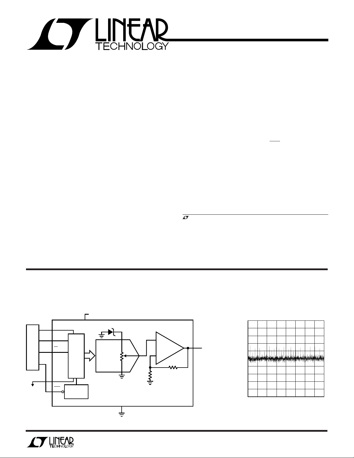
TYPICAL APPLICATION
Functional Block Diagram: 12-Bit Rail-to-Rail DAC with Clear Input
4.5V TO 5.5V
8
µP
TO
OTHER
DACS
D
2
IN
CLK1
CS/LD3
4
D
OUT
CLR6
V
12-BIT
SHIFT
REG
AND
DAC
LATCH
POWER-ON
RESET
2.048V
CC
12-BIT
DAC
U
GND
Differential Nonlinearity
vs Input Code
0.5
+
–
5
V
OUT
RAIL-TO-RAIL
7
VOLTAGE
OUTPUT
1456 TA01
0
DNL ERROR (LSB)
–0.5
512 1536 3072 3584
0
1024 2048 2560
CODE
4095
1456 TA02
1
Page 2
LTC1456
WW
W
U
ABSOLUTE MAXIMUM RATINGS
VCC to GND .............................................. –0.5V to 7.5V
Logic Inputs to GND ................................ –0.5V to 7.5V
V
.............................................. –0.5V to VCC + 0.5V
OUT
Maximum Junction Temperature ......... –65°C to 125°C
Operating Temperature Range
LTC1456C ............................................ 0°C to 70°C
LTC1456I ........................................ –40°C to 85°C
Storage Temperature Range ................ –65°C to 150°C
Lead Temperature (Soldering, 10 sec)................. 300°C
PACKAGE
TOP VIEW
CLK
1
D
2
IN
CS/LD
3
D
4
OUT
N8 PACKAGE
8-LEAD PDIP
T
= 125°C, θJA = 100°C/W (N8)
JMAX
T
= 125°C, θJA = 150°C/W (S8)
JMAX
/
O
RDER I FOR ATIO
V
8
CC
V
7
OUT
CLR
6
GND
5
S8 PACKAGE
8-LEAD PLASTIC SO
S8 PART MARKING
WU
ORDER PART
NUMBER
LTC1456CN8
LTC1456IN8
LTC1456CS8
LTC1456IS8
1456
1456I
Consult factory for Military grade parts.
ELECTRICAL CHARACTERISTICS
VCC = 4.5V to 5.5V, V
SYMBOL PARAMETER CONDITIONS MIN TYP MAX UNITS
DAC
Resolution ● 12 Bits
DNL Differential Nonlinearity Guaranteed Monotonic (Note 1) ● ±0.5 LSB
INL Integral Nonlinearity TA = 25°C ±3.5 LSB
V
OS
VOSTC Offset Error Temperature ±15 µV/°C
V
FS
VFSTC Full-Scale Voltage ±24 ppm/°C
Power Supply
V
CC
I
CC
Op Amp DC Performance
AC Performance
Offset Error TA = 25°C ±12 mV
Coefficient
Full-Scale Voltage TA = 25°C 4.065 4.095 4.125 V
Temperature Coefficient
Positive Supply Voltage For Specified Performance ● 4.5 5.5 V
Supply Current (Note 4) ● 430 650 µA
Short-Circuit Current Low V
Short-Circuit Current High V
Output Impedance to GND Input Code = 0 ● 40 120 Ω
Voltage Output Slew Rate (Note 2) ● 0.4 1.0 V/µs
Voltage Output Settling Time (Notes 2, 3) to ±0.5LSB 14 µs
Digital Feedthrough 0.3 nV• s
unloaded, TA = T
OUT
to T
MIN
(Note 1)
Shorted to GND ● 120 mA
OUT
Shorted to V
OUT
, unless otherwise noted.
MAX
CC
● ±4 LSB
● ±18 mV
● 4.045 4.095 4.145 V
● 120 mA
U
2
Page 3
LTC1456
ELECTRICAL CHARACTERISTICS
VCC = 4.5V to 5.5V, V
SYMBOL PARAMETER CONDITIONS MIN TYP MAX UNITS
Digital I/O
V
IH
V
IL
V
OH
V
OL
I
LEAK
C
IN
Switching
t
1
t
2
t
3
t
4
t
5
t
6
t
7
t
8
t
9
t
10
Digital Input High Voltage ● 2.4 V
Digital Input Low Voltage ● 0.8 V
Digital Output High Voltage I
Digital Output Low Voltage I
Digital Input Leakage VCC = 5V, VIN = GND to V
Digital Input Capacitance Guaranteed by Design. Not Subject to Test. ● 10 pF
DIN Valid to CLK Setup ● 40 ns
DIN Valid to CLK Hold ● 0ns
CLK High Time ● 40 ns
CLK Low Time ● 40 ns
CS/LD Pulse Width ● 50 ns
LSB CLK to CS/LD ● 40 ns
CS/LD Low to CLK ● 20 ns
D
Output Delay C
OUT
CLK Low to CS/LD Low ● 20 ns
CLR Pulse Width ● 65 ns
unloaded, TA = T
OUT
to T
MIN
= –1mA, D
OUT
= 1mA, D
OUT
= 15pF, VCC = 5V ● 150 ns
LOAD
, unless otherwise noted.
MAX
Only ● VCC – 1.0 V
OUT
Only ● 0.4 V
OUT
CC
● ±10 µA
The ● denotes specifications which apply over the full operating
temperature range.
Note 1: Nonlinearity is defined from the first code that is greater than or
equal to the maximum offset specification to code 4095 (full scale).
Note 2: Load is 5kΩ in parallel with 100pF.
Note 3: DAC switched between all 1s and the code corresponding to V
OS
for the part.
Note 4: Digital inputs at 0V or VCC.
3
Page 4

LTC1456
TEMPERATURE (°C)
–55
SUPPLY CURRENT (µA)
510
530
550
65
1456 G09
490
470
500
520
540
480
460
450
–25
5
35
95
125
VCC = 5.5V
VCC = 4.5V
VCC = 5V
UW
TYPICAL PERFORMANCE CHARACTERISTICS
Differential Nonlinearity (DNL)
0.5
0.4
0.3
0.2
0.1
0
DNL (LSB)
–0.1
–0.2
–0.3
–0.4
–0.5
1024 2048 2560
512 1536 3072 3584 4095
0
CODE
1456 G01
Integral Nonlinearity (INL)
2.0
1.6
1.2
0.8
0.4
0
–0.4
INL ERROR (LSB)
–0.8
–1.2
–1.6
–2.0
1024 2048 2560
512 1536 3072 3584 4095
0
CODE
1456 G02
Minimum Supply Headroom for
Full Output Swing vs Load Current
1.4
∆V
< 1LSB
OUT
CODE: ALL 1s
(V)
OUT
– V
CC
V
1.2
1.0
0.8
0.6
0.4
0.2
V
0
0
= 4.095V
OUT
510
LOAD CURRENT (mA)
20 30
15 25
1456 G03
Minimum Output Voltage
vs Output Sink Current
700
600
500
400
300
200
100
OUTPUT PULL-DOWN VOLTAGE (mV)
0
0
6
10
8
4
2
OUTPUT SINK CURRENT (mA)
125°C
25°C
–55°C
14
12 16
18
1456 G04
20
Output Swing vs Load Resistance Offset Voltage vs Temperature
4.5
CODE: ALL 1s
4.0
3.5
3.0
2.5
2.0
1.5
OUTPUT SWING (V)
1.0
0.5
0
10
4
100 1k 10k
LOAD RESISTANCE (Ω)
R
L
1456 G07
Supply Current
vs Logic Input Voltage Output Swing vs Load Resistance
1.750
1.615
1.480
1.345
1.210
1.075
0.940
0.805
SUPPLY CURRENT (mA)
0.670
0.535
0.400
1
0
1.5
0.5 4.5
LOGIC INPUT VOLTAGE (V)
ALL DIGITAL INPUTS
TIED TOGETHER
3
2
2.5
3.5
4
5
1456 G05
4.5
4.0
3.5
3.0
2.5
2.0
1.5
OUTPUT SWING (V)
1.0
0.5
0
10
100 1k 10k
LOAD RESISTANCE (Ω)
Supply Current vs Temperature
0.9
0.8
0.7
0.6
0.5
OFFSET VOLTAGE (mV)
0.4
0.3
–55
53565
–25
TEMPERATURE (°C)
95 125
1456 G08
CODE: ALL 0s
V
CC
R
L
1456 G06
Page 5

UUU
PIN FUNCTIONS
LTC1456
CLK (Pin 1): The Serial Interface Clock. Internal Schmitt
trigger on this input allows direct optocoupler interface.
D
(Pin 2): The Serial Interface Data. Data on the DIN pin
IN
is latched into the shift register on the rising edge of the
serial clock.
CS/LD (Pin 3): The Serial Interface Enable and Load
Control. When CS/LD is low the CLK signal is enabled, so
the data can be clocked in. When CS/LD is pulled high,
data is loaded from the shift register into the DAC
register, updating the DAC output. When CS/LD is high
the CLK is disabled internally.
W
BLOCK
IDAGRA
CLK
1
D
2
IN
3
CS/LD
12-BIT
SHIFT
REGISTER
LD
DAC
REGISTER
D
(Pin 4): The Output of the Shift Register Which
OUT
Becomes Valid on the Rising Edge of the Serial Clock.
GND (Pin 5): Ground.
CLR (Pin 6): The Clear Input. When pulled low, this pin
asynchronously clears the internal shift and DAC registers
to zero scale. Should be tied high for normal operation.
V
(Pin 7): The Buffered DAC Output.
OUT
V
(Pin 8): The Positive Supply Input. 4.5V ≤ VCC ≤ 5.5V.
CC
Requires a bypass capacitor to ground.
V
8
2.048V
12-BIT
DAC
+
–
CC
V
7
OUT
D
4
OUT
WU W
TI I G DIAGRA
CLK
t
9
D
CS/LD
D
OUT
IN
B0
PREVIOUS WORD
B11
PREVIOUS WORD
POWER-ON
t
1
RESET
B11
MSB
CLR
6
GND
5
1146 BD
t
2
B10
t
4
B10
t
8
t
3
B1
B1
t
6
B0
t
7
B0
LSB
t
5
B11
CURRENT WORD
1456 TD
5
Page 6

LTC1456
UU
DEFI ITIO S
Resolution (n): Resolution is defined as the number of
digital input bits, n. It defines the number of DAC output
states (2n) that divide the full-scale range. The resolution
does not imply linearity.
Full-Scale Voltage (VFS): This is the output of the DAC
when all bits are set to 1.
Voltage Offset Error (VOS): The theoretical voltage at the
output when the DAC is loaded with all zeros. The output
amplifier can have a true negative offset, but because the
part is operated from a single supply, the output cannot go
below zero. If the offset is negative, the output will remain
near 0V resulting in the transfer curve shown in Figure 1.
The offset of the part is measured at the code that corresponds to the maximum offset specification:
VOS = V
– [(Code • VFS)/(2n – 1)]
OUT
Least Significant Bit (LSB): One LSB is the ideal voltage
difference between two successive codes.
LSB = (VFS – VOS)/(2n – 1) = (VFS – VOS)/4095
LSB = 4.095/4095 = 1mV
Integral Nonlinearity (INL): End-point INL is the maximum deviation from a straight line passing through the
end-points of the DAC transfer curve. Because the part
operates from a single supply and the output cannot go
below zero, the linearity is measured between full scale
and the code corresponding to the maximum offset specification. The INL error at a given input code is calculated
as follows:
INL = [V
V
= The output voltage of the DAC measured at
OUT
– VOS – (VFS – VOS)(code/4095)]/LSB
OUT
the given input code
Differential Nonlinearity (DNL): DNL is the difference
between the measured change and the ideal 1LSB change
between any two adjacent codes. The DNL error between
any two codes is calculated as follows:
DNL = (∆V
∆V
= The measured voltage difference between
OUT
– LSB)/LSB
OUT
two adjacent codes
Digital Feedthrough: The glitch that appears at the analog
output caused by AC coupling from the digital inputs when
they change state. The area of the glitch is specified in
(nV)(sec).
6
OUTPUT
VOLTAGE
NEGATIVE
OFFSET
0V
Figure 1. Effect of Negative Offset
DAC CODE
1456 F01
Page 7

OPERATIO
D
IN
CLK
CS/LD
D
OUT
µP
0.1µF
OUTPUT
0V TO 4.095V
V
CC
V
OUT
GND
LTC1456
CLR
TO NEXT DAC FOR
DAISY-CHAINING
4.5V TO 5.5V
1456 TA03
LTC1456
U
Serial Interface
The data on the DIN input is loaded into the shift register
on the rising edge of the clock. The MSB is loaded first. The
DAC register loads the data from the shift register when
CS/LD is pulled high. The CLK is disabled internally when
CS/LD is high. Note: CLK must be low before CS/LD is
pulled low to avoid an extra internal clock pulse.
When CLR is pulled low it asynchronously resets the shift
and DAC registers to all zeros.
The buffered output of the 12-bit shift register is available
on the D
pin which swings from GND to VCC. Multiple
OUT
LTC1456s may be daisy-chained together by connecting
the D
pin to the DIN pin of the next chip, while the CLK
OUT
U
TYPICAL APPLICATION
The circuit below shows a digitally programmable current
source from an external voltage source using an external
op amp, an LT®1077 and an NPN transistor (2N3440). Any
digital word from 0 to 4095 is loaded into the LTC1456 and
its output correspondingly swings from 0V to 4.095V. In
the configuration shown, this voltage will be forced across
the resistor RA. If RA is chosen to be 410Ω the output
current will range from 0mA at zero scale to 10mA at full
scale. The minimum voltage for VS is determined by the
load resistor RL and Q1’s V
resistor of 50Ω, the voltage source can be as low as 5V.
voltage. With a load
CESAT
and CS/LD signals remain common to all chips in the daisy
chain. The serial data is clocked to all of the chips, then the
CS/LD signal is pulled high to update all of them simultaneously.
Voltage Output
The LTC1456's rail-to-rail buffered output can source or
sink 5mA over the entire operating temperature range
while pulling to within 300mV of the positive supply
voltage or ground. The output swings to within a few
millivolts of either supply rail when unloaded and has an
equivalent output resistance of 40Ω when driving a load to
the rails. The output can drive 1000pF without going into
oscillation.
12-Bit 5V Single Supply Voltage Output DAC
µP
Digitally Programmable Current Source
5V
+ 5V TO 100V
V
S
≤ 50Ω
FOR R
0.1µF
CLR
CLK
D
CS/LD
Information furnished by Linear Technology Corporation is believed to be accurate and reliable.
However, no responsibility is assumed for its use. Linear Technology Corporation makes no representation that the interconnection of its circuits as described herein will not infringe on existing patent rights.
V
CC
LTC1456
IN
GND
V
OUT
+
LT1077
–
L
R
Q1
2N3440
R
410Ω
LIOUT
A
4096 • R
1456 TA04
DIN • 4.095
= ≈ 0mA TO 10mA
A
7
Page 8

LTC1456
PACKAGE DESCRIPTION
0.300 – 0.325
(7.620 – 8.255)
U
Dimensions in inches (millimeters) unless otherwise noted.
N8 Package
8-Lead PDIP (Narrow 0.300)
(LTC DWG # 05-08-1510)
0.045 – 0.065
(1.143 – 1.651)
0.130 ± 0.005
(3.302 ± 0.127)
876
0.400*
(10.160)
MAX
5
0.065
(1.651)
0.009 – 0.015
(0.229 – 0.381)
+0.025
0.325
–0.015
+0.635
8.255
()
–0.381
*THESE DIMENSIONS DO NOT INCLUDE MOLD FLASH OR PROTRUSIONS.
MOLD FLASH OR PROTRUSIONS SHALL NOT EXCEED 0.010 INCH (0.254mm)
TYP
0.005
(0.127)
MIN
0.100 ± 0.010
(2.540 ± 0.254)
8-Lead Plastic Small Outline (Narrow 0.150)
0.010 – 0.020
(0.254 – 0.508)
0.008 – 0.010
(0.203 – 0.254)
*
DIMENSION DOES NOT INCLUDE MOLD FLASH. MOLD FLASH
SHALL NOT EXCEED 0.006" (0.152mm) PER SIDE
**
DIMENSION DOES NOT INCLUDE INTERLEAD FLASH. INTERLEAD
FLASH SHALL NOT EXCEED 0.010" (0.254mm) PER SIDE
× 45°
0.016 – 0.050
0.406 – 1.270
0.053 – 0.069
(1.346 – 1.752)
0°– 8° TYP
(0.355 – 0.483)
0.014 – 0.019
0.125
(3.175)
MIN
0.018 ± 0.003
(0.457 ± 0.076)
S8 Package
(LTC DWG # 05-08-1610)
0.004 – 0.010
(0.101 – 0.254)
0.050
(1.270)
BSC
0.015
(0.380)
MIN
(5.791 – 6.197)
0.255 ± 0.015*
(6.477 ± 0.381)
0.228 – 0.244
12
0.189 – 0.197*
(4.801 – 5.004)
7
8
1
2
4
3
N8 0695
5
6
0.150 – 0.157**
(3.810 – 3.988)
SO8 0695
3
4
RELATED PARTS
PART NUMBER DESCRIPTION COMMENTS
LTC1257 Single 12-Bit V
Reference Can Be Overdriven Up to 12V, i.e., FS
LTC1446/LTC1446L Dual 12-Bit V
LTC1450/LTC1450L Single 12-Bit V
LTC1451 Single Rail-to-Rail 12-Bit DAC, Full Scale: 4.095V, VCC: 4.5V to 5.5V, Same as LTC1456 Except REF Out Pin Replaces
Internal 2.048V Reference Brought Out to Pin CLR Pin
LTC1452 Single Rail-to-Rail 12-Bit V
LTC1453 Single Rail-to-Rail 12-Bit V
LTC1454/LTC1454L Dual 12-Bit V
LTC1458/LTC1458L Quad 12 Bit Rail-to-Rail Output DACs with Added Functionality LTC1458: VCC = 4.5V to 5.5V, V
Linear Technology Corporation
8
1630 McCarthy Blvd., Milpitas, CA 95035-7417 ● (408) 432-1900
FAX: (408) 434-0507
●
TELEX: 499-3977 ● www.linear-tech.com
DAC, Full Scale: 2.048V, VCC: 4.75V to 15.75V, 5V to 15V Single Supply, Complete V
OUT
DACs in SO-8 Package LTC1446: VCC = 4.5V to 5.5V, V
OUT
DACs with Parallel Interface LTC1450: VCC = 4.5V to 5.5V, V
OUT
Multiplying DAC, VCC: 2.7V to 5.5V Low Power, Multiplying V
OUT
= 12V SO-8 Package
MAX
LTC1446L: V
LTC1450L: V
= 2.7V to 5.5V, V
CC
= 2.7V to 5.5V, V
CC
OUT
Buffer Amplifier in SO-8 Package
DAC, Full Scale: 2.5V, VCC: 2.7V to 5.5V 3V, Low Power, Complete V
OUT
DACs in SO-16 Package with Added Functionality LTC1454: VCC = 4.5V to 5.5V, V
OUT
LTC1454L: V
LTC1458L: V
= 2.7V to 5.5V, V
CC
= 2.7V to 5.5V, V
CC
1456fs, sn1456 LT/TP 0697 7K • PRINTED IN
LINEAR TECHNOLOGY CORPORATION 1996
DAC in
OUT
= 0V to 4.095V
OUT
= 0V to 2.5V
OUT
= 0V to 4.095V
OUT
= 0V to 2.5V
OUT
DAC with Rail-to-Rail
DAC in SO-8 Package
OUT
= 0V to 4.095V
OUT
= 0V to 2.5V
OUT
= 0V to 4.095V
OUT
= 0V to 2.5V
OUT
USA
 Loading...