

Page 1
FEATURES
LTC1451
LTC1452/LTC1453
12-Bit Rail-to-Rail
Micropower DACs in SO-8
U
DESCRIPTIO
■
12-Bit Resolution
■
Buffered True Rail-to-Rail Voltage Output
■
3V Operation (LTC1453), ICC: 250µA Typ
■
5V Operation (LTC1451), ICC: 400µA Typ
■
3V to 5V Operation (LTC1452), ICC: 225µA Typ
■
Built-In Reference: 2.048V (LTC1451)
1.220V (LTC1453)
■
Multiplying Version (LTC1452)
■
Power-On Reset
■
SO-8 Package
■
3-Wire Cascadable Serial Interface
■
Maximum DNL Error: 0.5LSB
■
Schmitt Trigger on Clock Input Allows Direct
Optocoupler Interface
U
APPLICATIO S
■
Digital Calibration
■
Industrial Process Control
■
Automatic Test Equipment
■
Cellular Telephones
The LTC®1451/LTC1452/LTC1453 are complete single
supply, rail-to-rail voltage output 12-bit digital-to-analog
converters (DACs) in an SO-8 package. They include an
output buffer amplifier and an easy-to-use 3-wire
cascadable serial interface.
The LTC1451 has an onboard reference of 2.048V and a
full-scale output of 4.095V. It operates from a single 4.5V
to 5.5V supply.
The LTC1452 is a multiplying DAC with a full-scale output
of twice the reference input voltage. It operates from a
single supply of 2.7V to 5.5V.
The LTC1453 has an onboard 1.22V reference and a fullscale output of 2.5V. It operates from a single supply of
2.7V to 5.5V.
The low power supply current makes the LTC1451 family
ideal for battery-powered applications. The space saving
8-pin SO package and operation with no external components provide the smallest 12-bit DAC system available.
, LTC and LT are registered trademarks of Linear Technology Corporation.
TYPICAL APPLICATIO
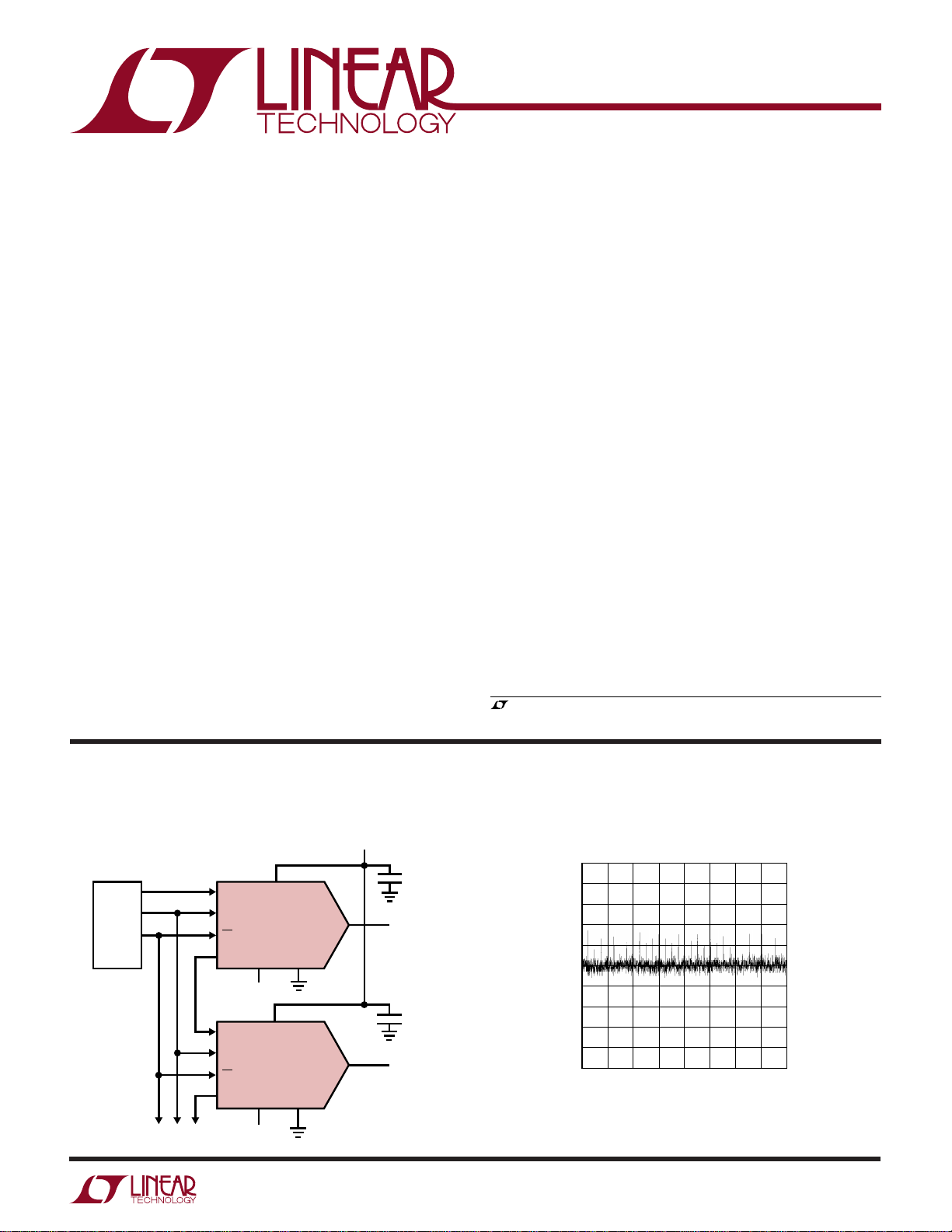
Daisy-Chained Control Outputs
V
µP
D
CLK
CS/LD
D
D
CLK
CS/LD
D
TO NEXT DAC
IN
OUT
IN
OUT
LTC1451
V
REF
LTC1451
V
REF
CC
GND
V
CC
GND
U
V
V
OUT
OUT
Differential Nonlinearity
5V
0.1µF
CONTROL
OUTPUT 1
0.1µF
CONTROL
OUTPUT 2
1451/2/3 TA01
0.5
0.0
DNL ERROR (LSB)
–0.5
0
vs Input Code
1024 2048 2560
512 1536 3072 3584
CODE
1451/2/3 TA02
4095
1
Page 2
LTC1451
LTC1452/LTC1453
WWWU
ABSOLUTE AXI U RATI GS
(Note 1)
VCC to GND .............................................. –0.5V to 7.5V
TTL Input Voltage .................................... –0.5V to 7.5V
V
OUT
, D
.................................... –0.5V to VCC + 0.5V
OUT
REF ................................................ –0.5V to VCC + 0.5V
Maximum Junction Temperature ......... –65°C to 125°C
UU
W
PACKAGE/ORDER I FOR ATIO
TOP VIEW
CLK
1
D
2
IN
CS/LD
3
D
4
OUT
N8 PACKAGE
8-LEAD PDIP
T
= 125°C, θJA = 100°C/W (N8)
JMAX
T
= 125°C, θJA = 150°C/W (S8)
JMAX
Consult factory for Military grade parts.
8-LEAD PLASTIC SO
V
8
CC
V
7
OUT
REF
6
GND
5
S8 PACKAGE
LTC1451CN8
LTC1452CN8
LTC1453CN8
LTC1451IN8
LTC1452IN8
LTC1453IN8
Operating Temperature Range
Commercial ...........................................0°C to 70°C
Industrial ......................................... –40°C to 85°C
Storage Temperature Range ................ –65°C to 150°C
Lead Temperature (Soldering, 10 sec)................. 300°C
ORDER PART NUMBER
LTC1451CS8
LTC1452CS8
LTC1453CS8
LTC1451IS8
LTC1452IS8
LTC1453IS8
S8 PART MARKING
1451
1452
1453
1451I
1452I
1453I
ELECTRICAL CHARACTERISTICS
temperature range, otherwise specifications are at TA = 25°C. VCC = 4.5V to 5.5V (LTC1451), 2.7V to 5.5V (LTC1452/LTC1453),
internal or external reference (V
SYMBOL PARAMETER CONDITIONS MIN TYP MAX UNITS
DAC
Resolution ● 12 Bits
DNL Differential Nonlinearity Guaranteed Monotonic (Note 2) ● ±0.5 LSB
INL Integral Nonlinearity TA = 25°C ±3.5 LSB
V
OS
VOSTC Offset Error Temperature ±15 µV/°C
V
FS
VFSTC Full-Scale Voltage When Using Internal Reference, LTC1451 ±0.10 LSB/°C
Offset Error TA = 25°C ±12 mV
Coefficient
Full-Scale Voltage When Using Internal Reference, LTC1451, TA = 25°C 4.065 4.095 4.125 V
Temperature Coefficient When Using External 2.048V Reference, LTC1452 ±0.02 LSB/°C
≤ VCC/2), V
REF
(Note 2)
LTC1451
External 2.048V Reference, VCC = 5V, LTC1452 ● 4.075 4.095 4.115 V
When Using Internal Reference, LTC1453, TA = 25°C 2.470 2.500 2.530 V
LTC1453
When Using Internal Reference, LTC1453 ±0.10 LSB/°C
and REF unloaded, unless otherwise noted.
OUT
The ● denotes specifications which apply over the full operating
● ±4LSB
● ±18 mV
● 4.045 4.095 4.145 V
● 2.460 2.500 2.540 V
2
Page 3
LTC1451
LTC1452/LTC1453
ELECTRICAL CHARACTERISTICS
The ● denotes specifications which apply over the full operating
temperature range, otherwise specifications are at TA = 25°C. VCC = 4.5V to 5.5V (LTC1451), 2.7V to 5.5V (LTC1452/LTC1453),
internal or external reference (V
SYMBOL PARAMETER CONDITIONS MIN TYP MAX UNITS
Reference (LTC1451/LTC1453)
Reference Output Voltage LTC1451 ● 2.008 2.048 2.088 V
Reference Output ±0.08 LSB/°C
Temperature Coefficient
Reference Line Regulation ● 0.7 ±2LSB/V
Reference Load Regulation 0 ≤ I
Reference Input Range V
Reference Input Resistance ● 81430 kΩ
Reference Input Capacitance 15 pF
Short-Circuit Current REF Shorted to GND ● 80 mA
Power Supply
V
CC
I
CC
Op Amp DC Performance
AC Performance
SINAD Signal-to-Noise + Distortion REF = 1kHz, 2V
Positive Supply Voltage For Specified Performance, LTC1451 ● 4.5 5.5 V
Supply Current 4.5V ≤ VCC ≤ 5.5V (Note 4), LTC1451 ● 300 400 620 µA
Short-Circuit Current Low V
Short-Circuit Current High V
Output Impedance to GND Input Code = 0 ● 40 120 Ω
Voltage Output Slew Rate (Note 3) ● 0.4 1.0 V/µs
Voltage Output Settling Time (Notes 3, 4) to ±0.5LSB 14 µs
Digital Feedthrough 0.3 nV• s
AC Feedthrough REF = 1kHz, 2V
≤ VCC/2), V
REF
LTC1453
LTC1453
REF
LTC1452
LTC1453
2.7V ≤ V
2.7V ≤ V
OUT
OUT
and REF unloaded, unless otherwise noted.
OUT
≤ 100µA, LTC1451 ● 0.2 ±1.5 LSB
OUT
≤ VCC – 1.5V ● VCC/2 V
≤ 5.5V (Note 4), LTC1452 ● 120 225 350 µA
CC
≤ 5.5V (Note 4), LTC1453 ● 150 250 500 µA
CC
Shorted to GND ● 100 mA
Shorted to V
CC
, LTC1452 –95 dB
P-P
, (Code: All 1s) LTC1452 85 dB
P-P
● 1.195 1.220 1.245 V
● 0.6 ±3 LSB
● 2.7 5.5 V
● 2.7 5.5 V
● 120 mA
3
Page 4
LTC1451
LTC1452/LTC1453
ELECTRICAL CHARACTERISTICS
The ● denotes specifications which apply over the full operating
temperature range, otherwise specifications are at TA = 25°C. VCC = 5V (LTC1451LTC1452), VCC = 3V (LTC1453).
LTC1451/LTC1452 LTC1453
SYMBOL PARAMETER CONDITIONS MIN TYP MAX MIN TYP MAX UNITS
Digital I/O
V
IH
V
IL
V
OH
V
OL
I
LEAK
C
IN
Switching
t
1
t
2
t
3
t
4
t
5
t
6
t
7
t
8
t
9
Digital Input High Voltage ● 2.4 2.0 V
Digital Input Low Voltage ● 0.8 0.6 V
Digital Output High Voltage I
Digital Output Low Voltage I
Digital Input Leakage VIN = GND to V
= –1mA ● VCC – 1.0 VCC – 0.7 V
OUT
= 1mA ● 0.4 0.4 V
OUT
CC
● ±10 ±10 µA
Digital Input Capacitance Guaranteed by Design ● 10 10 pF
Not Subject to Test
DIN Valid to CLK Setup ● 40 60 ns
DIN Valid to CLK Hold ● 00 ns
CLK High Time ● 40 60 ns
CLK Low Time ● 40 60 ns
CS/LD Pulse Width ● 50 80 ns
LSB CLK to CS/LD ● 40 60 ns
CS/LD Low to CLK ● 20 30 ns
D
Output Delay C
OUT
= 15pF ● 150 220 ns
LOAD
CLK Low to CS/LD Low ● 20 30 ns
Note 1: Absolute Maximum Ratings are those values beyond which the life
of the device may be impaired.
Note 2: Nonlinearity is defined from the first code that is greater than or
equal to the maximum offset specification to code 4095 (full scale).
Note 3: Load is 5kΩ in parallel with 100pF.
Note 4: DAC switched between all 1s and the code corresponding to V
for the part, i.e., LTC1451: code 18; LTC1453: code 30.
Note 5: Digital inputs at 0V or VCC.
UW
TYPICAL PERFOR A CE CHARACTERISTICS
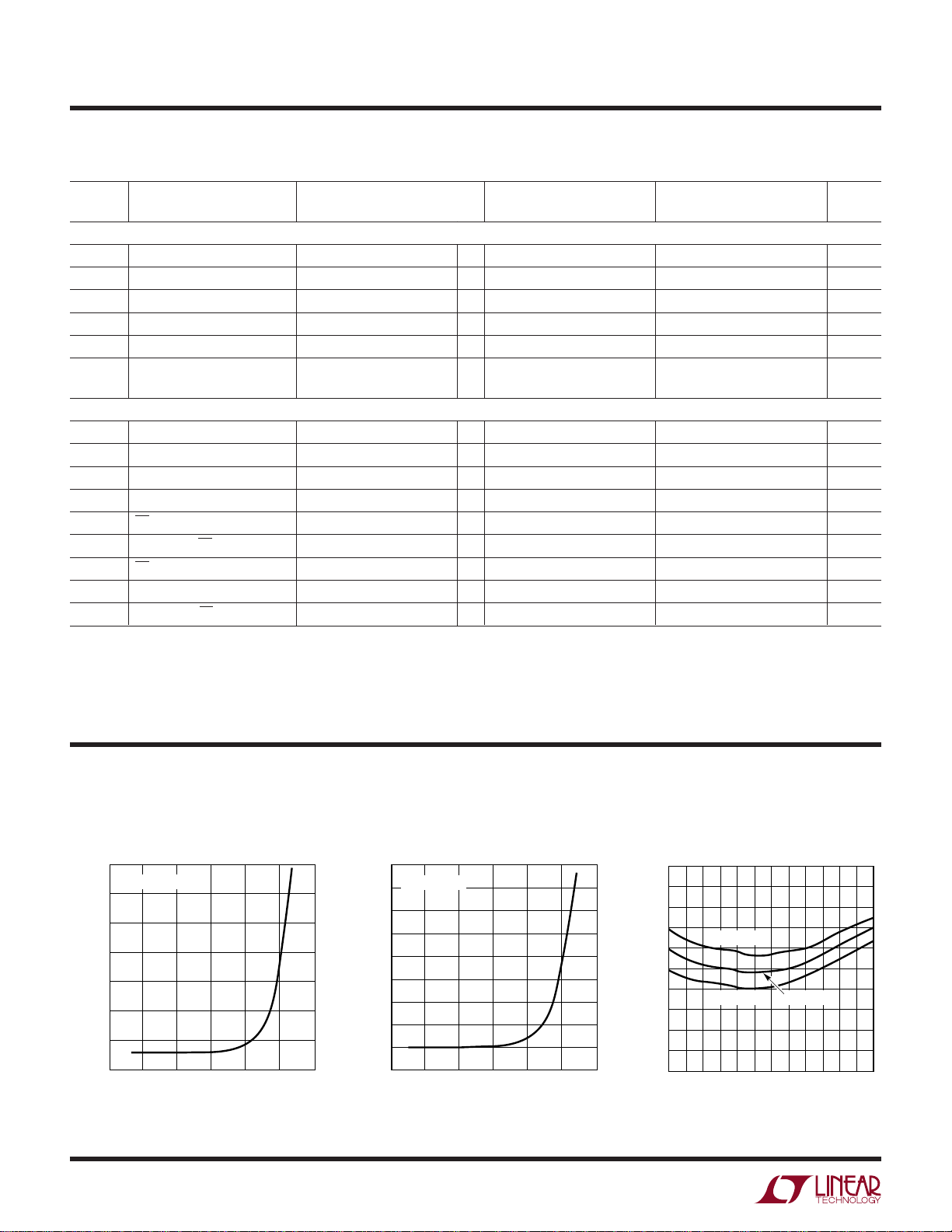
LTC1451 Minimum Supply
Voltage vs Load Current
5.4
∆V
< 1LSB
OUT
5.2
5.0
4.8
4.6
4.4
MINIMUM SUPPLY VOLTAGE (V)
4.2
4.0
0.0001
0.010.001 0.1 100
LOAD CURRENT (mA)
110
1451/2/3 G01
LTC1453 Minimum Supply
Voltage vs Load Current
4.50
∆V
< 1LSB
0.0001
OUT
0.010.001 0.1 100
LOAD CURRENT (mA)
4.25
4.00
3.75
3.50
3.25
3.00
2.75
MINIMUM SUPPLY VOLTAGE (V)
2.50
2.25
110
1451/2/3 G02
LTC1451
Supply Current vs Temperature
450
440
430
420
410
400
390
380
SUPPLY CURRENT (µA)
370
360
350
–55
VCC = 5.5V
VCC = 4.5V VCC = 5V
–25
35 65
5
TEMPERATURE (°C)
95
1451/2/3 G03
OS
125
4
Page 5

UW
TYPICAL PERFOR A CE CHARACTERISTICS
LTC1451
LTC1452/LTC1453
LTC1451
Supply Current vs Logic Input
Voltage
1.15
1.05
0.95
0.85
0.75
0.65
SUPPLY CURRENT (mA)
0.55
0.45
0.35
1.0 1.5 2.5 3.5 4.50.5
0
LOGIC INPUT VOLTAGE (V)
ALL DIGITAL INPUTS
TIED TOGETHER
3.0
2.0
LTC1451
Offset Voltage vs Temperature
900
800
700
600
500
OFFSET VOLTAGE (µV)
400
300
–55
–25
35 65
5
TEMPERATURE (°C)
4.0
95
1451/2/3 G04
1451/2/3 G07
5.0
125
LTC1451
Output Swing vs Load Resistance
4.5
4.0
3.5
3.0
2.5
2.0
1.5
OUTPUT SWING (V)
1.0
0.5
0
10
100 1k 10k
LOAD RESISTANCE (Ω)
FULL SCALE
TIED TO GND
R
L
ZERO SCALE
TIED TO V
R
L
LTC1451
Differential Nonlinearity (DNL)
0.5
0.0
DNL ERROR (LSB)
–0.5
1024 2048 2560
512 1536 3072 3584
0
CODE
VCC = 5V
CC
1451/2/3 G05
1451/2/3 TA02
4095
LTC1451
Pull-Down Voltage vs Output Sink
Current Capability
1000
100
10
1
OUTPUT PULL-DOWN VOLTAGE (mV)
0.1
0.0001 0.1 1 10 100
0.001 0.01
OUTPUT SINK CURRENT (mA)
125°C
25°C
–55°C
1451/2/3 G06
LTC1451
Integral Nonlinearity (INL)
2.0
1.6
1.2
0.8
0.4
0
–0.4
ERROR (LSB)
–0.8
VCC = 5V
–1.2
INTERNAL REFERENCE
–1.6
–2.0
= 25°C
T
A
0
512 1536
1024
2048
CODE
2560
3072
3584
1451/2/3 G09
4095
LTC1452
Total Harmonic Distortion + Noise
vs Frequency
–40
VCC = 5V
= 2V
V
IN
–50
–60
–70
–80
–90
TOTAL HARMONIC DISTORTION + NOISE (dB)
–100
P-P
V
= 4V
OUT
P-P
10050 10k 100k
1k
FREQUENCY (Hz)
1451/2/3 G08
0.2LSB/DIV
LTC1451
Broadband Output Noise
CODE = FFFH
BW = 3Hz TO 1.4MHz
GAIN = 1000
5ms/DIV
1451/2/3 G10
5
Page 6

LTC1451
LTC1452/LTC1453
U
UU
PI FU CTIO S
CLK: The TTL Level Input for the Serial Interface Clock.
DIN: The TTL Level Input for the Serial Interface Data. Data
on the DIN pin is latched into the shift register on the rising
edge of the serial clock.
CS/LD: The TTL Level Input for the Serial Interface Enable
and Load Control. When CS/LD is low the CLK signal is
enabled, so the data can be clocked in. When CS/LD is
pulled high, data is loaded from the shift register into the
DAC register, updating the DAC output.
D
: The Output of the Shift Register which Becomes
OUT
Valid on the Rising Edge of the Serial Clock.
W
BLOCK DIAGRA
CLK
1
GND: Ground.
REF: The Output of the Internal Reference and the Input
to the DAC Resistor Ladder. An external reference with
voltage up to VCC/2 may be used for the LTC1452.
V
: The Buffered DAC Output.
OUT
VCC: The Positive Supply Input. 4.5V ≤ VCC ≤ 5.5V
(LTC1451), 2.7 ≤ VCC ≤ 5.5V (LTC1452/LTC1453). Requires a bypass capacitor to ground.
V
8
CC
D
2
IN
3
CS/LD
D
4
OUT
UWW
TI I G DIAGRA
CLK
D
CS/LD
IN
B0
PREVIOUS WORD
LD
12-BIT
SHIFT
REGISTER
POWER-ON
t
1
t
9
RESET
B11
MSB
DAC
REGISTER
t
2
12-BIT DAC
REFERENCE
LTC1451: 2.048V
LTC1453: 1.22V
B10
t
8
t
4
+
V
7
OUT
–
REF
6
GND
5
11451/2/3 BD
t
6
t
3
B1
B0
LSB
t
7
t
5
6
D
OUT
B11
PREVIOUS WORD
B10
B1
B0
B11
CURRENT WORD
1451/2/3 TD
Page 7

DEFI ITIO S
LTC1451
LTC1452/LTC1453
UU
Resolution (n): Resolution is defined as the number of
digital input bits, n. It defines the number of DAC output
states (2n) that divide the full-scale range. The resolution
does not imply linearity.
Full-Scale Voltage (VFS): This is the output of the DAC
when all bits are set to 1.
Voltage Offset Error (VOS): Normally, DAC offset is the
voltage at the output when the DAC is loaded with all zeros.
The DAC can have a true negative offset, but because the
part is operated from a single supply, the output cannot go
below zero. If the offset is negative, the output will remain
near 0V resulting in the transfer curve shown in Figure 1.
The offset of the part is measured at the code that corresponds to the maximum offset specification:
VOS = V
– [(Code × VFS)/(2n – 1)]
OUT
Least Significant Bit (LSB): One LSB is the ideal voltage
difference between two successive codes.
LSB = (VFS – VOS)/(2n – 1) = (VFS – VOS)/4095
Nominal LSBs:
LTC1451 LSB = 4.095V/4095 = 1mV
LTC1452 LSB = V(REF)/4095
LTC1453 LSB = 2.5V/4095 = 0.610mV
Integral Nonlinearity (INL): End-point INL is the maximum deviation from a straight line passing through the
end-points of the DAC transfer curve. Because the part
operates from a single supply and the output cannot go
below zero, the linearity is measured between full scale
and the code corresponding to the maximum offset specification. The INL error at a given input code is calculated
as follows:
INL = [V
V
= The output voltage of the DAC measured at
OUT
– VOS – (VFS – VOS)(code/4095)]/LSB
OUT
the given input code
Differential Nonlinearity (DNL): DNL is the difference
between the measured change and the ideal 1LSB change
between any two adjacent codes. The DNL error between
any two codes is calculated as follows:
DNL = (∆V
∆V
= The measured voltage difference between
OUT
– LSB)/LSB
OUT
two adjacent codes
Digital Feedthrough: The glitch that appears at the analog
output caused by AC coupling from the digital inputs when
they change state. The area of the glitch is specified in
nV × sec.
OUTPUT
VOLTAGE
NEGATIVE
OFFSET
0V
Figure 1. Effect of Negative Offset
DAC CODE
1451/2/3 F01
7
Page 8

LTC1451
LTC1452/LTC1453
U
OPERATIO
Serial Interface
The data on the DIN input is loaded into the shift register
on the rising edge of the clock. The MSB is loaded first. The
DAC register loads the data from the shift register when
CS/LD is pulled high. The CLK is disabled internally when
CS/LD is high. Note: CLK must be low before CS/LD is
pulled low to avoid an extra internal clock pulse.
The buffered output of the 12-bit shift register is available
on the D
Multiple LTC1451/LTC1452/LTC1453s may be daisychained together by connecting the D
pin of the next chip, while the CLK and CS/LD signals
remain common to all chips in the daisy chain. The serial
data is clocked to all of the chips, then the CS/LD signal is
pulled high to update all of them simultaneously.
pin which swings from GND to VCC.
OUT
OUT
pin to the D
IN
Reference
The LTC1451 includes an internal 2.048V reference, making 1LSB equal to 1mV (gain of 2). The LTC1453 has an
internal reference of 1.22V with a full scale of 2.5V (gain of
2.05). The internal reference output is turned off when the
pin is forced above the reference voltage, allowing an
external reference to be connected to the reference pin.
The LTC1452 has no internal reference and the REF pin
must be driven externally. The buffer gain is 2, so the
external reference must be less than VCC/2 and be capable
of driving the 8k minimum DAC resistor ladder.
Voltage Output
The LTC1451 family’s rail-to-rail buffered output can
source or sink 5mA over the entire operating temperature
range while pulling to within 300mV of the positive supply
voltage or ground. The output swings to within a few
millivolts of either supply rail when unloaded and has an
equivalent output resistance of 40Ω when driving a load to
the rails. The output can drive 1000pF without going into
oscillation.
8
Page 9

TYPICAL APPLICATIO S
®
1121-3.3
LT
OUTIN
1µF
FROM
OPTO-
ISOLATED
INPUTS
3.3V
OPTO-ISOLATORS
CLK
D
CS/LD
IN
500Ω
4N28
U
An Isolated 4mA to 20mA Process Controller
Has 3.3V Minimum Loop Voltage
90k 5k
V
10k
CLK
D
IN
CS/LD
CLK
D
IN
CS/LD
V
CC
LTC1453
REF
OUT
45k 5k
V
LTC1451
LTC1452/LTC1453
V
LOOP
3.3V TO 30V
+
3k
LT1077
–
1k
Q1
2N3440
R
S
10Ω
I
OUT
11451/2/3 TA04
This circuit shows how to use an LTC1453 to make an
opto-isolated digitally controlled 4mA to 20mA process
controller. The controller circuitry, including the optoisolation, is powered by the loop voltage that can have a
wide range of 3.3V to 30V. The 1.22V reference output of
the LTC1453 is used for the 4mA offset current and V
OUT
is used for the digitally controlled 0mA to 16mA current.
RS is a sense resistor and the op amp modulates the
transistor Q1 to provide the 4mA to 20mA current through
this resistor. The potentiometers allow for offset and fullscale adjustment. The control circuitry dissipates well
under the 4mA budget at zero-scale.
Note that although these DACs have internal Schmitt
triggers and are suitable for use with slow rising edges
such as produced by the above optoisolator, the use of
optoisolators in a daisy-chained topology requires the
addition of a gate or the use of a fast isolator on the clock
signal. Setup and hold times between D
and DIN are not
OUT
guaranteed unless a clock edge with a rise time of less than
100ns is provided.
9
Page 10

LTC1451
LTC1452/LTC1453
TYPICAL APPLICATIO S
U
12-Bit 3V to 5V Voltage Output DAC
LTC1451: 4.5V TO 5.5V
LTC1452: 2.7V TO 5.5V
LTC1453: 2.7V TO 5.5V
0.1µF
OUTPUT
LTC1451: 0V TO 4.095V
LTC1452: 0V TO 2 • REF
LTC1453: 0V TO 2.5V
1451/2/3 TA03
µP
TO NEXT DAC FOR
DAISY-CHAINING
V
D
CLK
CS/LD
D
LTC1451: 2.048V
LTC1452: EXTERNAL
LTC1453: 1.22V
IN
OUT
LTC145X
V
REF
CC
GND
V
OUT
Digitally Programmable Current Source
5V
+ 5V TO 100V
V
S
FOR R
≤ 50Ω
0.1µF
V
CLK
µP
D
CS/LD
CC
LTC1451
IN
GND
V
OUT
+
LT1077
–
L
R
Q1
2N3440
LIOUT
4096 • R
DIN • 4.095
= ≈ 0mA TO 10mA
A
This circuit shows a digitally programmable current source
from an external voltage source using an external op amp,
an LT1077 and an NPN transistor (2N3440). Any digital
word from 0 to 4095 is loaded into the LTC1451 and its
output correspondingly swings from 0V to 4.095V. In the
configuration shown, this voltage will be forced across the
10
R
A
410Ω
1451/2/3 TA05
resistor RA. If RA is chosen to be 410Ω the output current
will range from 0mA at zero-scale to 10mA at full-scale.
The minimum voltage for VS is determined by the load
resistor RL and Q1's V
voltage. With a load resistor
CESAT
of 50Ω, the voltage source can be as low as 5V.
Page 11

PACKAGE DESCRIPTIO
LTC1452/LTC1453
U
Dimensions in inches (millimeters) unless otherwise noted.
N8 Package
8-Lead PDIP (Narrow 0.300)
(LTC DWG # 05-08-1510)
0.400*
(10.160)
MAX
876
0.255 ± 0.015*
(6.477 ± 0.381)
5
LTC1451
12
0.300 – 0.325
(7.620 – 8.255)
0.065
(1.651)
0.009 – 0.015
(0.229 – 0.381)
+0.035
0.325
–0.015
+0.889
8.255
()
–0.381
*THESE DIMENSIONS DO NOT INCLUDE MOLD FLASH OR PROTRUSIONS.
MOLD FLASH OR PROTRUSIONS SHALL NOT EXCEED 0.010 INCH (0.254mm)
TYP
0.045 – 0.065
(1.143 – 1.651)
0.100
(2.54)
BSC
S8 Package
8-Lead Plastic Small Outline (Narrow 0.150)
(LTC DWG # 05-08-1610)
8
0.228 – 0.244
(5.791 – 6.197)
3
0.189 – 0.197*
(4.801 – 5.004)
7
6
4
0.130 ± 0.005
(3.302 ± 0.127)
0.125
(3.175)
MIN
0.018 ± 0.003
(0.457 ± 0.076)
5
0.150 – 0.157**
(3.810 – 3.988)
0.020
(0.508)
MIN
N8 1098
0.010 – 0.020
(0.254 – 0.508)
0.008 – 0.010
(0.203 – 0.254)
*
DIMENSION DOES NOT INCLUDE MOLD FLASH. MOLD FLASH
SHALL NOT EXCEED 0.006" (0.152mm) PER SIDE
**
DIMENSION DOES NOT INCLUDE INTERLEAD FLASH. INTERLEAD
FLASH SHALL NOT EXCEED 0.010" (0.254mm) PER SIDE
Information furnished by Linear Technology Corporation is believed to be accurate and reliable.
However, no responsibility is assumed for its use. Linear Technology Corporation makes no representation that the interconnection of its circuits as described herein will not infringe on existing patent rights.
× 45°
0°– 8° TYP
0.016 – 0.050
(0.406 – 1.270)
0.053 – 0.069
(1.346 – 1.752)
0.014 – 0.019
(0.355 – 0.483)
TYP
1
3
2
4
0.004 – 0.010
(0.101 – 0.254)
0.050
(1.270)
BSC
SO8 1298
11
Page 12

LTC1451
LTC1452/LTC1453
TYPICAL APPLICATION
U
This circuit shows how to make a bipolar output 12-bit
DAC with a wide output swing using an LTC1451 and an
LT1077. R1 and R2 resistively divide down the LTC1451
output and an offset is summed in using the LTC1451
onboard 2.048V reference and R3 and R4. R5 ensures that
A Wide Swing, Bipolar Output 12-Bit DAC
5V
0.1µF
V
µP
4.094
V
OUT
–4.096
CLK
D
CS/LD
2048 4095
IN
LTC1451
GND V
D
IN
CC
V
OUT
REF
R3
10k
R5
20k
the onboard reference is always sourcing current and
never has to sink any current even when V
is at full-
OUT
scale. The LT1077 output will have a wide bipolar output
swing of – 4.096V to 4.094V as shown in the figure above.
With this output swing 1LSB = 2mV.
R1
5k
R2
10k
+
LT1077
–
5V
–5V
R4
20k
V
OUT
1451/2/3 TA06
2 • DIN • 4.095
:
4096
– 4.096V
RELATED PARTS
PART NUMBER DESCRIPTION COMMENTS
LTC1257 5V to 15V Single Supply, Complete 12-Bit V
OUT
DAC in SO-8 Package
LTC1446/LTC1446L Dual 12-Bit V
LTC1448 Dual 12-Bit V
LTC1655/LTC1655L 5V/3V 16-Bit V
LTC1659 Single 12-Bit V
LTC7541 12-Bit Multiplying Parallel I
LTC7543/LTC8143 12-Bit Multiplying Serial I
LTC8043 12-Bit Multiplying Serial I
DACs in SO-8 5V with 4.096V Full-Scale Output/3V with 2.5V Full Scale
OUT
DAC in SO-8 VCC from 2.7V to 5.5V, Output Swings to V
OUT
DAC in SO-8 Pin Conpatible with LTC1451/LTC1453
OUT
DAC in MSOP VCC from 2.7V to 5.5V, Output Swings to V
OUT
DAC 5V to 16V Supply, 12-Bit Wide Interface
OUT
DAC 5V Supply, Clear Pin and Serial Data Output (LTC8143)
OUT
DAC 5V Supply, SO-8 Package
OUT
Linear Technology Corporation
12
1630 McCarthy Blvd., Milpitas, CA 95035-7487
(408) 432-1900
●
FAX
: (408) 434-0507
●
TELEX
: 499-3977
Reference Can Be Overdriven Up to 12V, i.e., FS MAX = 12V
REF
REF
145123fa LT/TP 0100 2K REV A • PRINTED IN USA
LINEAR TECHNOLOGY CORPORATION 1995
 Loading...