

Page 1
LTC1446/LTC1446L
Dual 12-Bit Rail-to-Rail
Micropower DACs in SO-8
EATU
F
■
Dual DACs with 12-Bit Resolution
■
SO-8 Package
■
Rail-to-Rail Output Amplifiers
■
3V Operation (LTC1446L): ICC = 650µA Typ
■
5V Operation (LTC1446): ICC = 1000µA Typ
■
Internal Reference
■
Power-On Reset Clears DACs to 0V
■
3-Wire Cascadable Serial Interface
■
Maximum DNL Error: 0.5LSB
■
Low Cost
■
Schmitt Trigger On Input Allows Direct
RE
S
Optocoupler Interface
U
O
PPLICATI
A
■
Digital Calibration
■
Industrial Process Control
■
Automatic Test Equipment
■
Cellular Telephones
S
DUESCRIPTIO
The LTC®1446/LTC1446L are dual 12-bit digital-to-analog
converters (DACs) available in an SO-8 package. They are
complete with a rail-to-rail voltage
internal reference and an easy-to-use 3-wire cascadable
serial interface.
The LTC1446 has an internal reference and a full-scale
output of 4.095V. It operates from a single 4.5V to 5.5V
supply.
The LTC1446L has an internal reference and a full-scale
output of 2.5V. It operates from a single 2.7V to 5.5V
supply.
The low power supply current makes the LTC1446 family
ideal for battery-powered applications. These DACs are
available in space saving 8-pin SO and PDIP packages and
require no external components for operation.
, LTC and LT are registered trademarks of Linear Technology Corporation.
output amplifier, an
U
O
A
PPLICATITYPICAL
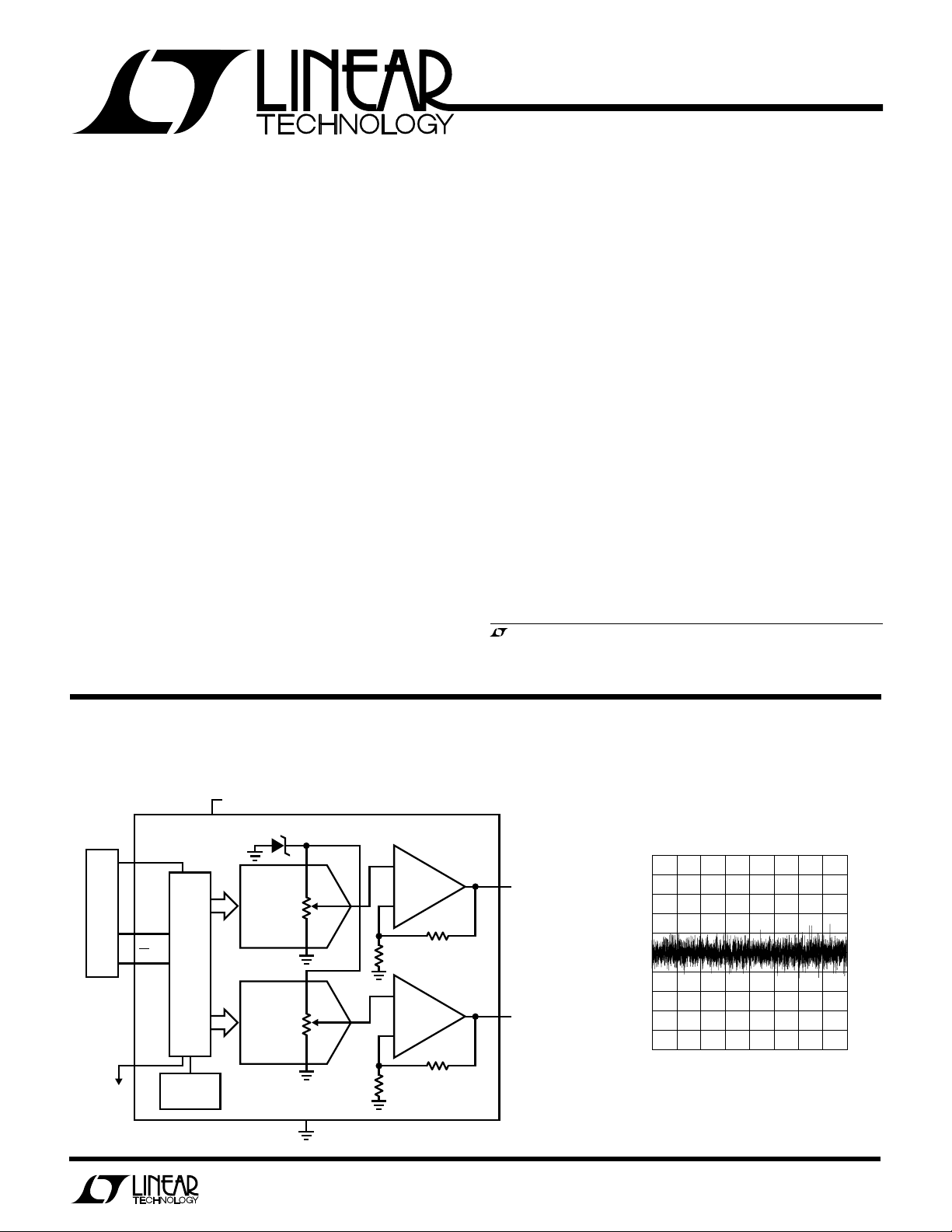
Functional Block Diagram: Dual 12-Bit Rail-to-Rail DAC
LTC1446: 5V
LTC1446L: 3V TO 5V
7
V
CC
DIN2
µP
CLK1
24-BIT
SHIFT
CS/LD3
REG
AND
DAC
LATCH
4
D
OUT
POWER-ON
RESET
12-BIT
DAC B
12-BIT
DAC A
GND
6
+
–
+
–
V
OUT B
V
OUT A
1446/1446L TA01
8
RAIL-TO-RAIL
VOLTAGE
OUTPUT
5
Differential Nonlinearity vs Input Code
0.5
0.4
0.3
0.2
0.1
0
–0.1
DNL ERROR (LSB)
–0.2
–0.3
–0.4
–0.5
1024 2048 2560
512 1536 3072 3584 4095
0
CODE
1446/46L G13
1
Page 2
LTC1446/LTC1446L
A
W
O
LUTEXI T
S
A
WUW
ARB
U
G
I
S
VCC to GND................................................ –0.5 to 7.5V
Logic Inputs to GND................................... –0.5 to 7.5V
Operating Temperature Range
LTC1446C/LTC1446LC............................0°C to 70°C
LTC1446I/LTC1446LI ..........................–40°C to 85°C
U
W
PACKAGE/ORDER INFORMATION
ORDER PART
TOP VIEW
1
CLK
D
2
IN
CS/LD
3
D
4
OUT
N8 PACKAGE
8-LEAD PDIP
T
= 125°C, θJA = 100°C/W
JMAX
Consult factory for Military grade parts.
V
8
OUT B
V
7
CC
GND
6
V
5
OUT A
NUMBER
LTC1446CN8
LTC1446IN8
LTC1446LCN8
LTC1446LIN8
V
OUT A/VOUT B
.................................–0.5V to VCC + 0.5V
Maximum Junction Temperature..........................125°C
Storage Temperature Range ..................–65°C to 150°C
Lead Temperature (Soldering, 10 sec)................. 300°C
U
ORDER PART
NUMBER
LTC1446CS8
LTC1446IS8
LTC1446LCS8
LTC1446LIS8
S8 PART MARKING
1446C 1446LC
1446I 1446LI
1
CLK
D
2
IN
CS/LD
3
D
4
OUT
8-LEAD PLASTIC SO
= 125°C, θJA = 150°C/W
T
JMAX
TOP VIEW
S8 PACKAGE
V
8
OUT B
V
7
CC
GND
6
V
5
OUT A
ELECTRICAL CHARACTERISTICS
VCC = 4.5V to 5.5V (LTC1446), 2.7V to 5.5V (LTC1446L), V
SYMBOL PARAMETER CONDITIONS MIN TYP MAX UNITS
DAC
Resolution ● 12 Bits
DNL Differential Nonlinearity Guaranteed Monotonic (Note 1) ● ±0.2 ±0.5 LSB
INL Integral Nonlinearity TA = 25°C ±2.0 4.5 LSB
ZSE Zero-Scale Error ● 0 3 18 mV
V
OS
V
TC Offset Error Tempco ±15 µV/°C
OS
V
FS
V
TC Full-Scale Voltage Tempco ±0.1 LSB/°C
FS
Power Supply (LTC1446)
V
CC
I
CC
Power Supply (LTC1446L)
V
CC
I
CC
Offset Error ● ±2 ±18 mV
Full-Scale Voltage LTC1446, TA = 25°C 4.065 4.095 4.125 V
LTC1446 ● 4.045 4.095 4.145 V
LTC1446L, T
LTC1446L ● 2.460 2.500 2.540 V
Positive Supply Voltage For Specified Performance ● 4.5 5.5 V
Supply Current 4.5V ≤ V
Positive Supply Voltage For Specified Performance ● 2.7 5.5 V
Supply Current 2.7V ≤ V
and V
OUT A
= 25°C 2.470 2.500 2.530 V
A
≤ 5.5V (Note 4) ● 1000 1500 µA
CC
≤ 5.5V (Note 4) ● 650 1000 µA
CC
unloaded, TA = T
OUT B
to T
MIN
● ±2.5 5.0 LSB
unless otherwise noted.
MAX,
2
Page 3
LTC1446/LTC1446L
ELECTRICAL CHARACTERISTICS
VCC = 4.5V to 5.5V (LTC1446), 2.7V to 5.5V (LTC1446L), V
SYMBOL PARAMETER CONDITIONS MIN TYP MAX UNITS
Op Amp DC Performance
Short-Circuit Current Low V
Short-Circuit Current High V
Output Impedance to GND Input Code = 0 ● 40 120 Ω
AC Performance
Voltage Output Slew Rate (Note 2) ● 0.5 1 V/µs
Voltage Output Settling Time (Notes 2, 3) to ±0.5LSB 14 µs
OUT
OUT
and V
OUT A
Shorted to GND ● 55 120 mA
Shorted to V
unloaded, TA = T
OUT B
CC
to T
MIN
● 70 120 mA
unless otherwise noted.
MAX,
VCC = 5V (LTC1446), VCC = 3V (LTC1446L), TA = T
SYMBOL PARAMETER CONDITIONS MIN TYP MAX MIN TYP MAX UNITS
Digital I/O
V
IH
V
IL
V
OH
V
OL
I
LEAK
C
IN
Switching
t
1
t
2
t
3
t
4
t
5
t
6
t
7
t
8
t
9
Digital Input High Voltage ● 2.4 2 V
Digital Input Low Voltage ● 0.8 0.6 V
Digital Output High Voltage I
Digital Output Low Voltage I
Digital Input Leakage VIN = GND to V
Digital Input Capacitance Guaranteed by Design ● 10 10 pF
DIN Valid to CLK Setup ● 40 60 ns
DIN Valid to CLK Hold ● 00ns
CLK High Time ● 40 60 ns
CLK Low Time ● 40 60 ns
CS/LD Pulse Width ● 50 80 ns
LSB CLK to CS/LD ● 40 60 ns
CS/LD Low to CLK ● 20 30 ns
D
Output Delay C
OUT
CLK Low to CS/LD Low ● 20 30 ns
= –1mA ● VCC – 1.0 VCC – 0.7 V
OUT
= 1mA ● 0.4 0.4 V
OUT
= 15pF ● 150 220 ns
LOAD
MIN
to T
CC
unless otherwise noted.
MAX,
LTC1446 LTC1446L
● ±10 ±10 µA
The
● denotes specifications which apply over the full operating
temperature range.
Note 1: Nonlinearity is defined from the first code that is greater
than or equal to the maximum offset specification to code 4095
(full scale).
Note 2: Load is 5kΩ in parallel with 100pF.
Note 3: DAC switched between all 1s and the code corresponding
to VOS for the part.
Note 4: Digital inputs at 0V or VCC.
3
Page 4
LTC1446/LTC1446L
CODE
0
–0.5
DNL ERROR (LSB)
–0.4
–0.2
–0.1
0
0.5
0.2
1024 2048 2560
1446/46L G03
–0.3
0.3
0.4
0.1
512 1536 3072 3584 4095
LOAD CURRENT (mA)
0
0
V
CC
– V
OUT
0.2
0.4
0.6
0.8
1.2
510
LTC1446/46L • TPC06
15
1.0
∆V
OUT
< 1LSB
CODE: ALL 1's
V
OUT
= 2.5V
LOGIC INPUT VOLTAGE (V)
0.6
SUPPLY CURRENT (mA)
1.4
2.2
3.0
1.0
1.8
2.6
1234
1446/46L G09
50
W
U
TYPICAL PERFORMANCE CHARACTERISTICS
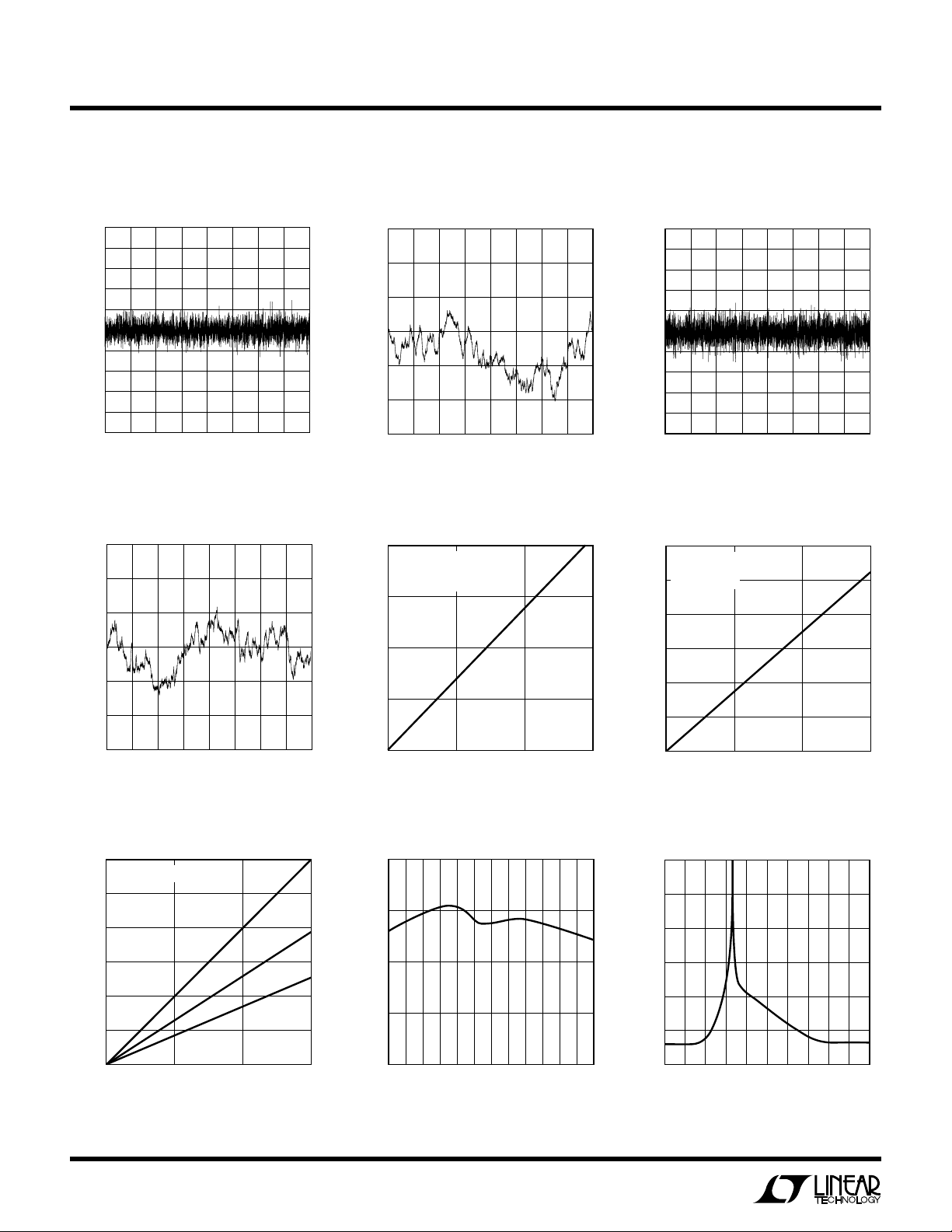
LTC1446 Differential Nonlinearity
(DNL) LTC1446 Integral Nonlinearity (INL) LTC1446L Differential Nonlinearity
0.5
0.4
0.3
0.2
0.1
0
–0.1
DNL ERROR (LSB)
–0.2
–0.3
–0.4
–0.5
1024 2048 2560
512 1536 3072 3584 4095
0
CODE
1446/46L G01
3
2
1
0
–1
INL ERROR (LSB)
–2
–3
512 1536
0
1024 2048
CODE
2560
3072
3584
1446/46L G02
4095
LTC1446L Integral Nonlinearity
3
2
1
0
–1
INL ERROR (LSB)
–2
–3
512 1536
0
1024 2048
LTC1446 Min Output Voltage vs
Output Sink Current
600
CODE: ALL 0'S
500
400
300
200
100
OUTPUT PULL-DOWN VOLTAGE (mV)
0
0
OUTPUT SINK CURRENT (mA)
4
3072
2560
CODE
125°C
510
25°C
–55°C
LTC1446/46L • TPC07
3584
1446/46L G04
4095
15
LTC1446 Min Supply Headroom for
Full Output Swing vs Load Current
0.8
∆V
< 1LSB
OUT
CODE: ALL 1's
= 4.095V
V
OUT
0.6
(V)
OUT
0.4
– V
CC
V
0.2
0
0
5
LOAD CURRENT (mA)
10
LTC1446 Full-Scale Voltage
vs Temperature
4.11
4.10
4.09
4.08
FULL-SCALE VOLTAGE (V)
4.07
–55
–25 5 35 65
TEMPERATURE (°C)
LTC1446L Min Supply Headroom for
Full Output Swing vs Load Current
15
LTC1446/46L • TPC05
LTC1446 Supply Current
vs Logic Input Voltage
95 125
1446/46L G09
Page 5

W
U
TYPICAL PERFORMANCE CHARACTERISTICS
LTC1446/LTC1446L
LTC1446L Supply Current vs Logic
Input Voltage
1.2
1.1
1.0
0.9
0.8
0.7
SUPPLY CURRENT (mA)
0.6
0.5
1.0 1.5 2.0 2.5 3.0
0.5
LOGIC INPUT VOLTAGE (V)
1446/46L G10
LTC1446 Supply Current vs
Temperature
970
960
950
940
930
920
SUPPLY CURRENT (µA)
910
900
–55 –35 –15 5 25 45 65 85 105
TEMPERATURE (°C)
UUU
PIN FUNCTIONS
CLK: The Serial Interface Clock.
DIN: The Serial Interface Data.
CS/LD: The Serial Interface Enable and Load Control.
When CS/LD is low the CLK signal is enabled, so the data
can be clocked in. When CS/LD is pulled high data is
loaded from the shift register into the DAC registers,
updating the DAC outputs.
LTC1446L Supply Current
vs Temperature
700
690
680
VCC = 5.5V
VCC = 5V
VCC = 4.5V
125
1446/46L G11
D
: The output of the shift register which becomes valid
OUT
670
660
650
SUPPLY CURRENT (µA)
640
630
620
VCC = 3.3V
VCC = 3V
VCC = 2.7V
25
–55
–35 125
–15
TEMPERATURE (°C)
45
5
65
85
105
1446/46L G12
on the rising edge of the serial clock.
GND: Ground.
V
OUT A,VOUT B
: Buffered DAC Outputs.
VCC: Positive Supply Input.
4.5V ≤ V
≤ 5.5V (LTC1446), 2.7V ≤ V
CC
CC
≤ 5.5V
(LTC1446L). Requires a bypass capacitor to ground.
5
Page 6

LTC1446/LTC1446L
W
BLOCK DIAGRAM
REFERENCE
1
CLK
D
2
IN
CS/LD
3
D
4
OUT
UW W
TI I G DIAGRA
24-BIT
SHIFT
REGISTER
POWER-ON
RESET
LD
DAC B
REGISTER
LD
DAC A
REGISTER
12-BIT
DAC B
12-BIT
DAC A
+
V
8
OUT B
–
7V
CC
GND
6
+
V
5
OUT A
–
1446BD
CS/LD
6
D
CLK
D
OUT
IN
t
B0-B
PREVIOUS WORD
PREVIOUS WORD
9
B11-A
B11-A
MSB
B10-A
PREVIOUS WORD
t
t
4
B0-A
PREVIOUS WORD
B0-A
t
8
t
3
LSB
1
B11-B
PREV WORD
B11-B
MSB
t
2
B10-B
PREV WORD
B0-B
B0-B
PREV WORD
LSB
t
6
t
7
t
5
B11-A
CURRENT WORD
1446 TD
Page 7

UU
DEFI ITIO S
LTC1446/LTC1446L
Resolution (n)
Resolution is defined as the number of digital input bits,
n. It defines the number of DAC output states (2n) that
divide the full-scale range. The resolution does not imply
linearity.
Full-Scale Voltage (VFS)
This is the output of the DAC when all bits are set to one.
Voltage Offset Error (VOS)
The theoretical voltage at the output when the DAC is
loaded with all zeros. The output amplifier can have a true
negative offset, but because the part is operated from a
single supply, the output cannot go below zero. If the
offset is negative, the output will remain near 0V resulting
in the transfer curve shown in Figure 1.
OUTPUT
VOLTAGE
NEGATIVE
0V
OFFSET
Figure 1. Effect of Negative Offset
DAC CODE
1446/46L F01
The offset of the part is measured at the code that corresponds to the maximum offset specification:
V
= V
OS
– [(Code)(VFS)/(2n – 1)]
OUT
Least Significant Bit (LSB)
One LSB is the ideal voltage difference between two
successive codes.
Nominal LSBs:
LTC1446 LSB = 4.095V/4095 = 1mV
LTC1446L LSB = 2.5V/4095 = 0.610mV
Zero Scale Error (ZSE)
The output voltage when the DAC is loaded with all zeros.
Since this is a single supply part this value cannot be less
than 0V.
Integral Nonlinearity (INL)
End-point INL is the maximum deviation from a straight
line passing through the end points of the DAC transfer
curve. Because the part operates from a single supply and
the output cannot go below 0, the linearity is measured
between full scale and the code corresponding to the
maximum offset specification. The INL error at a given
input code is calculated as follows :
INL = [V
V
= the output voltage of the DAC measured at the given
OUT
– VOS – (VFS – VOS)(Code/4095)]/LSB
OUT
input code
Differential Nonlinearity (DNL)
DNL is the difference between the measured change and
the ideal 1LSB change between any two adjacent codes.
The DNL error between any two codes is calculated as
follows:
DNL = (∆V
∆V
OUT
= The measured voltage difference between two
– LSB)/LSB
OUT
adjacent codes
LSB = (VFS – VOS)/(2n – 1) = (VFS – VOS)/4095
7
Page 8

LTC1446/LTC1446L
U
OPERATIO
Serial Interface
The data on the DIN input is loaded into the shift register
on the rising edge of the clock. Data is loaded as one 24bit word where the first 12 bits are for DAC A and the
second 12 are for DAC B. For each 12-bit segment the MSB
is loaded first. Data from the shift register is loaded into the
DAC register when CS/LD is pulled high. The clock is
disabled internally when CS/LD is high. Note: CLK must be
low before CS/LD is pulled low to avoid an extra internal
clock pulse.
The buffered output of the 24-bit shift register is available
on the D
Multiple LTC1446/LTC1446L’s may be daisy-chained together by connecting the D
chip, while the clock and CS/LD signals remain common
to all chips in the daisy chain. The serial data is clocked to
all of the chips, then the CS/LD signal is pulled high to
update all of them simultaneously.
pin which swings from GND to VCC.
OUT
pin to the DIN pin of the next
OUT
Voltage Output
The LTC1446/LTC1446L include an internal voltage reference which is connected to each DAC. The LTC1446 has a
full scale of 4.095V making 1LSB equal to 1mV. The
LTC1446L has a full scale of 2.5V making 1LSB equal to
0.61mV.
The LTC1446/LTC1446L rail-to-rail buffered outputs can
source or sink 5mA when operating with a 5V supply while
pulling to within 300mV of the positive supply voltage or
ground. The outputs swing to within a few millivolts of
either supply rail when unloaded and have an equivalent
output resistance of 40Ω when driving a load to the rails.
The buffer amplifiers can drive 1000pF without going into
oscillation.
8
Page 9

U
TYPICAL APPLICATIONS N
LTC1446/LTC1446L
This circuit shows how to use an LTC1446 and an
LT®1077 to make a wide bipolar output swing 12-bit DAC
with an offset that can be digitally programmed. V
OUT A
,
which can be set by loading the appropriate digital code
A Wide Swing, Bipolar Output DAC with Digitally Controlled Offset
LTC1446
V
V
OUT B
V
GND
OUT A
CC
CLK
D
IN
µP
CS/LD
D
OUT
for DAC A, sets the offset. As this value changes, the
transfer curve for the output moves up and down as
illustrated in the graph below.
5V
0.1µF
15V
50k
50k
100k
+
LT1077
–
–15V
100k
V
2 (V
OUT
=
OUT B
– V
OUT A)
V
OUT
–4.096
–8.190
8.190
4.094
A
B
0
C
≅
A: V
B: V
C: V
OUT A
OUT A
OUT A
0V
≅
2.048V
≅
4.095V
1446/46L F02
D
IN
9
Page 10

LTC1446/LTC1446L
U
TYPICAL APPLICATIONS N
This circuit shows how to use one LTC1446 to make an
autoranging ADC. The microprocessor sets the reference
span and the Common pin for the analog input by loading
the appropriate digital code into the LTC1446. V
OUT A
controls the Common pin for the analog inputs to the
LTC1296 and V
controls the reference span by setting
OUT B
An Autoranging 8-Channel ADC with Shutdown
CS
D
OUT
µP
CLK
D
IN
22µF
+
V
LTC1296
SSO REF
5V
CC
CH0
CH7
COM
REF
–
the REF+ pin on the LTC1296. The LTC1296 has a Shutdown pin that goes low in shutdown mode. This will turn
off the PNP transistor supplying power to the LTC1446.
The resistor and capacitor on the LTC1446 outputs act as
a lowpass filter for noise.
8 ANALOG
INPUT CHANNELS
+
CLK
D
IN
CS/LD
D
OUT
74HC04
LTC1446
V
V
OUT B
V
GND
OUT A
50k
CC
100Ω
100Ω
50k
0.1µF
0.1µF
0.1µF
5V
1446/46L F03
10
Page 11

PACKAGE DESCRIPTION
LTC1446/LTC1446L
U
Dimensions in inches (millimeters) unless otherwise noted.
N8 Package
8-Lead PDIP (Narrow 0.300)
(LTC DWG# 05-08-1510)
0.400*
(10.160)
MAX
0.255 ± 0.015*
(6.477 ± 0.381)
876
5
12
0.300 – 0.325
(7.620 – 8.255)
0.065
(1.651)
0.009 – 0.015
(0.229 – 0.381)
+0.025
0.325
–0.015
+0.635
8.255
()
–0.381
*THESE DIMENSIONS DO NOT INCLUDE MOLD FLASH OR PROTRUSIONS.
MOLD FLASH OR PROTRUSIONS SHALL NOT EXCEED 0.010 INCH (0.254mm)
TYP
0.100 ± 0.010
(2.540 ± 0.254)
0.045 – 0.065
(1.143 – 1.651)
0.005
(0.127)
MIN
S8 Package
8-Lead Plastic Small Outline (Narrow 0.150)
(LTC DWG # 05-08-1610)
3
0.189 – 0.197*
(4.801 – 5.004)
8
7
4
0.130 ± 0.005
(3.302 ± 0.127)
0.125
(3.175)
MIN
0.018 ± 0.003
(0.457 ± 0.076)
5
6
0.015
(0.380)
MIN
N8 0695
0.010 – 0.020
(0.254 – 0.508)
0.008 – 0.010
(0.203 – 0.254)
*
DIMENSION DOES NOT INCLUDE MOLD FLASH. MOLD FLASH
SHALL NOT EXCEED 0.006" (0.152mm) PER SIDE
**
DIMENSION DOES NOT INCLUDE INTERLEAD FLASH. INTERLEAD
FLASH SHALL NOT EXCEED 0.010" (0.254mm) PER SIDE
× 45°
0°– 8° TYP
0.016 – 0.050
0.406 – 1.270
Information furnished by Linear Technology Corporation is believed to be accurate and reliable.
However, no responsibility is assumed for its use. Linear Technology Corporation makes no representation that the interconnection of its circuits as described herein will not infringe on existing patent rights.
0.228 – 0.244
(5.791 – 6.197)
0.053 – 0.069
(1.346 – 1.752)
0.014 – 0.019
(0.355 – 0.483)
0.150 – 0.157**
(3.810 – 3.988)
1
3
2
4
(0.101 – 0.254)
0.050
(1.270)
BSC
0.004 – 0.010
SO8 0695
11
Page 12

LTC1446/LTC1446L
RELATED PARTS
PART NUMBER DESCRIPTION COMMENTS
LTC1257 Single 12-Bit V
Reference Can Be Overdriven up to 12V, i.e., FS Max = 12V
LTC1451 Single Rail-to-Rail Output 12-Bit DAC, Low Power, Complete V
Full Scale: 4.095V, VCC: 4.5V to 5.5V Internal 2.048V Reference
Brought Out to Pin
LTC1452 Single Rail-to-Rail 12-Bit V
LTC1453 Single Rail-to-Rail 12-Bit V
Full Scale: 2.5V, V
LTC1454/LTC1454L Dual 12-Bit V
with Added Functionality LTC1454L: V
LTC1456 Single Rail-to-Rail Output 12-Bit DAC with Clear Pin Low Power, Complete V
Full Scale: 4.095V, V
LTC1458/LTC1458L Quad 12-Bit V
DAC, Full Scale: 2.048V, VCC: 4.75V to 15.75V, 5V to 15V Single Supply, Complete V
OUT
Mulitplying DAC, VCC: 2.7V to 5.5V Low Power, Mulitplying V
OUT
Amplifier in SO-8 Package
DAC, 3V, Low Power, Complete V
OUT
: 2.7V to 5.5V
CC
DACs in a 16-Lead SO Package LTC1454: VCC = 4.5V to 5.5V, V
OUT
: 4.5V to 5.5V with Clear Pin
CC
DACs in 28-Lead SW and SSOP Packages LTC1458: VCC = 4.5V to 5.5V, V
OUT
LTC1458L: V
= 2.7V to 5.5V, V
CC
= 2.7V to 5.5V, V
CC
DAC in SO-8 Package
OUT
DAC in SO-8 Package
OUT
DAC with Rail-to-Rail Buffer
OUT
DAC in SO-8 Package
OUT
= 0V to 4.095V
OUT
= 0V to 2.5V
OUT
DAC in SO-8 Package
OUT
= 0V to 4.095V
OUT
= 0V to 2.5V
OUT
12
Linear Technology Corporation
1630 McCarthy Blvd., Milpitas, CA 95035-7417
(408) 432-1 900
●
FAX
: (408) 434-0507
●
TELEX
: 499-3977
LT/GP 1096 7K • PRINTED IN USA
LINEAR TECHNOLOGY CORPORATION 1996
 Loading...