

Datasheet LTC1445IN, LTC1445CS, LTC1445CN, LTC1444IS, LTC1444CN Datasheet (Linear Technology)
...Page 1
FEATURES
■
Ultralow Quiescent Current: 8.5µA Max
■
Wide Supply Range
Single: 2V to 11V
Dual: ±1V to ±5.5V
■
Input Voltage Range Includes the Negative Supply
■
Reference Output Drives 0.01µF Capacitor
■
Adjustable Hysteresis (LTC1444/LTC1445)
■
TTL/CMOS Compatible Outputs
■
Propagation Delay: 12µs (Typ) (10mV Overdrive)
■
No Crowbar Current
■
40mA Continuous Source Current
■
Pin Compatible Upgrades for MAX924 (LTC1443)
U
APPLICATIO S
■
Battery-Powered System Monitoring
■
Threshold Detectors
■
Window Comparators
■
Oscillator Circuits
LTC1443/LTC1444/LTC1445
Ultralow Power Quad
Comparators with Reference
U
DESCRIPTIO
The LTC®1443/LTC1444/LTC1445 are ultralow power quad
comparators with a built-in reference. The comparators
feature less than 8.5µA supply current over temperature,
an internal reference (1.182V ±1% for LTC1443 or 1.221V
±1% for LTC1444/LTC1445), programmable hysteresis
(LTC1444/LTC1445) and TTL/CMOS output (LTC1443/
LTC1445) that sinks and sources current (open-drain
output for LTC1444). The reference output can drive a
bypass capacitor of up to 0.01µF without oscillation.
The comparators operate from a single 2V to 11V supply
or a dual ±1V to ±5.5V supply (LTC1443). Comparator
hysteresis is easily programmable using two resistors and
the HYST pin (LTC1444/LTC1445). Each comparator’s
input operates from the negative supply to within 1.3V of
the positive supply. The LTC1443/LTC1445 comparator
output stage can continuously source up to 40mA. By
eliminating the cross-conducting current that normally
happens when the comparator changes logic states, power
supply glitches are eliminated.
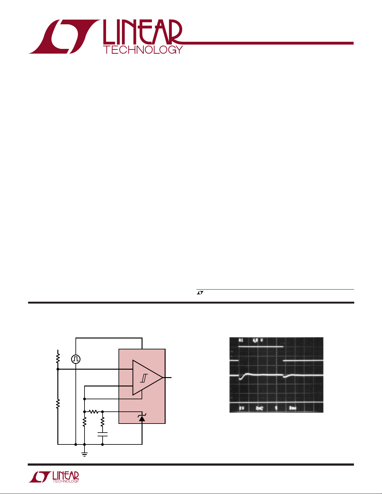
TYPICAL APPLICATIO
Reference Settling Test Circuit
V
IN
3.4M
1%
1.21M
1%
5V
TO 8V
R2
2.4M
R1
10k
5
4
14
8
R3
430Ω
C1
1.0µF
IN A
IN A
HYST
REF
U
+
–
+
–
3
+
V
LTC1445
–
V
9
LTC1443/44/45 • TA01
The LTC1443/LTC1444/LTC1445 are available in the
16-pin SO and PDIP packages.
, LTC and LT are registered trademarks of Linear Technology Corporation.
Reference Settling
8V
+
V
5V
2
OUT
V
REF
2mV/DIV
OUT
2ms/DIV
LTC1443/1444/1445 • TA02
1
Page 2
LTC1443/LTC1444/LTC1445
WWWU
ABSOLUTE AXI U RATI GS
(Note 1)
Voltage:
V+ to V–, V+ to GND, GND to V–...........12V to –0.3V
IN+, IN–, HYST................. (V+ + 0.3V) to (V– – 0.3V)
REF.................................. (V+ + 0.3V) to (V– – 0.3V)
OUT (LTC1443) ............. (V+ + 0.3V) to (GND – 0.3V)
OUT (LTC1444/LTC1445)
......................................... (V+ + 0.3V) to (V– – 0.3V)
Storage Temperature Range ................. –65°C to 150°C
Lead Temperature Range (Soldering, 10 sec)....... 300°C
UU
W
PACKAGE/ORDER I FOR ATIO
1
OUT B
2
OUT A
+
3
V
–
4
IN A
+
5
IN A
–
6
IN B
+
7
IN B
8
REF
N PACKAGE
16-LEAD PDIP
T
JMAX
T
JMAX
TOP VIEW
16
15
14
13
12
11
10
9
S PACKAGE
16-LEAD PLASTIC SO
= 150°C, θJA = 90°C/W (N)
= 150°C, θJA = 150°C/ W (S)
OUT C
OUT D
GND
IN D
IN D
IN C
IN C
–
V
+
–
+
–
ORDER PART
NUMBER
LTC1443CN
LTC1443CS
LTC1443IN
LTC1443IS
Current:
IN+, IN–, HYST.................................................. 20mA
REF................................................................... 20mA
OUT .................................................................. 50mA
OUT Short Circuit Duration (V+ ≤ 5.5V) ....... Continuous
Power Dissipation.............................................. 500mW
Operating Temperature Range
Commercial ............................................ 0°C to 70°C
Industrial ............................................ – 40°C to 85°C
1
OUT B
2
OUT A
+
3
V
–
4
IN A
+
5
IN A
–
6
IN B
+
7
IN B
8
REF
N PACKAGE
16-LEAD PDIP
T
JMAX
T
JMAX
TOP VIEW
16
15
14
13
12
11
10
9
S PACKAGE
16-LEAD PLASTIC SO
= 150°C, θJA = 90°C/W (N)
= 150°C, θJA = 150°C/ W (S)
OUT C
OUT D
HYST
IN D
IN D
IN C
IN C
–
V
+
–
+
–
ORDER PART
NUMBER
LTC1444CN
LTC1444CS
LTC1444IN
LTC1444IS
LTC1445CN
LTC1445CS
LTC1445IN
LTC1445IS
Consult factory for Military grade parts.
ELECTRICAL CHARACTERISTICS
The ● denotes the specifications which apply over the full operating
temperature range, otherwise specifications are at TA = 25°C. V+ = 5V, V– = GND = 0V, unless otherwise noted.
SYMBOL PARAMETER CONDITIONS MIN TYP MAX UNITS
Power Supply
+
V
I
CC
Comparator
V
OS
I
IN
V
CM
CMRR Common Mode Rejection Ratio V– to (V+ – 1.3V) 0.1 1.0 mV/V
PSRR Power Supply Rejection Ratio V+ = 2V to 11V 0.1 1.0 mV/V
Noise Voltage Noise 100Hz to 100kHz 20 µV
V
HYST
Supply Voltage Range ● 2.0 11.0 V
Supply Current IN+ = IN– = 80mV ● 5.5 8.5 µA
HYST = REF (LTC1444/LTC1445)
Comparator Input Offset Voltage VCM = 2.5V ● ±3.0 ±10.0 mV
+
Input Leakage Current (IN+, IN–)V
–
= V
IN
= 2.5V ● ±0.01 ±1.0 nA
IN
Input Leakage Current (HYST) LTC1444/LTC1445 ● ±0.02 ±1.0 nA
Comparator Input Common Mode Range ● V
–
V+ – 1.3V V
RMS
Hysteresis Input Voltage Range LTC1444, LTC1445 ● REF – 50mV REF V
2
Page 3
LTC1443/LTC1444/LTC1445
ELECTRICAL CHARACTERISTICS
The ● denotes the specifications which apply over the full operating
temperature range, otherwise specifications are at TA = 25°C. V+ = 5V, V– = GND = 0V, unless otherwise noted.
SYMBOL PARAMETER CONDITIONS MIN TYP MAX UNITS
t
PD
V
OH
V
OL
Propagation Delay Overdrive = 10mV, C
Overdrive = 100mV, C
= 100pF 12 µs
OUT
= 100pF 4 µs
OUT
Output High Voltage IO = –15mA; LTC1443/LTC1445 ● V+ – 0.4V V
Output Low Voltage IO = 1.8mA; LTC1443 ● GND + 0.4V V
IO = 1.8mA; LTC1444/LTC1445 ● V– + 0.4V V
Reference
V
REF
Reference Voltage No Load, LTC1443 C Temp Range ● 1.170 1.182 1.194 V
I Temp Range ● 1.164 1.200 V
No Load, LTC1444/ C Temp Range ● 1.209 1.221 1.233 V
I
SOURCE
I
SINK
LTC1445
Reference Output Source Current ∆V
Reference Output Sink Current ∆V
∆V
≤ 1mV ● 100 200 µA
REF
≤ 2.5mV 10 15 µA
REF
≤ 5mV ● 10 15 µA
REF
I Temp Range
Noise Voltage Noise 100Hz to 100kHz 100 µV
● 1.203 1.239 V
RMS
The ● denotes the specifications which apply over the full operating temperature range, otherwise specifications are at TA = 25°C.
V+ = 3V, V– = GND = 0V, unless otherwise noted.
SYMBOL PARAMETER CONDITIONS MIN TYP MAX UNITS
Power Supply
+
V
I
CC
Comparator
V
OS
I
IN
V
CM
CMRR Common Mode Rejection Ratio V– to (V+ –1.3V) 0.1 1.0 mV/V
PSRR Power Supply Rejection Ratio V+ = 2V to 11V 0.1 1.0 mV/V
Noise Voltage Noise 100Hz to 100kHz 100 µV
V
HYST
t
PD
V
OH
V
OL
Reference
V
REF
I
SOURCE
I
SINK
Noise Noise Voltage 100Hz to 100kHz 100 µV
Note 1: Absolute Maximum Ratings are those values beyond which the life
of the device may be impaired.
Supply Voltage Range ● 2.0 11.0 V
Supply Current IN+ = IN– = 80mV, HYST = REF ● 58 µA
Comparator Input Offset Voltage VCM = 1.5V ● ±3.0 ±10.0 mV
+
Input Leakage Current (IN+, IN–)V
–
= V
IN
= 1.5V ● ±0.01 ±1.0 nA
IN
Input Leakage Current (HYST) LTC1444/LTC1445 ● ±0.02 ±1.0 nA
Comparator Input Common Mode Range ● V
–
V+ – 1.3V V
RMS
Hysteresis Input Voltage Range LTC1444/LTC1445 ● REF – 50mV REF V
Propagation Delay Overdrive = 10mV, C
Overdrive = 100mV, C
= 100pF 14 µs
OUT
= 100pF 5 µs
OUT
Output High Voltage IO = –10mA, LTC1443/LTC1445 ● V+ – 0.4V V
Output Low Voltage IO = 0.8mA; LTC1443 ● GND + 0.4V V
IO = 0.8mA; LTC1444/LTC1445 ● V– + 0.4V V
Reference Voltage No Load, LTC1443 C Temp Range ● 1.170 1.182 1.194 V
I Temp Range ● 1.164 1.200 V
No Load, LTC1444/ C Temp Range ● 1.209 1.221 1.233 V
LTC1445
Reference Output Source Current ∆V
Reference Output Sink Current ∆V
∆V
I Temp Range
≤ 1mV ● 60 120 µA
REF
≤ 2.5mV 10 15 µA
REF
≤ 5mV ● 10 15 µA
REF
● 1.203 1.239 V
RMS
3
Page 4
LTC1443/LTC1444/LTC1445
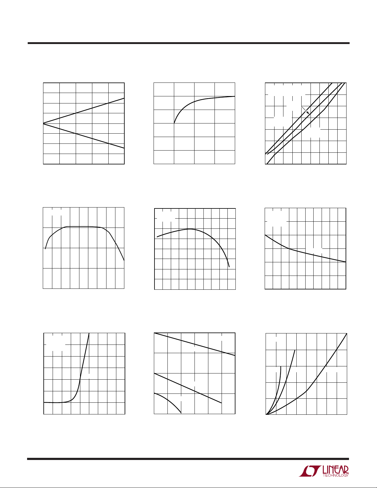
LOAD CURRENT (mA)
REFERENCE VOLTAGE (V)
1.184
1.183
1.182
1.181
1.180
1.179
1.178
0.2 0.4 0.6 0.8
LTC1443/44/45 • TPC06
1.00.10 0.3 0.5 0.7 0.9
V+ = 5V
V
–
= GND
T
A
= 25°C
SOURCE
UW
TYPICAL PERFOR A CE CHARACTERISTICS
LTC1444/LTC1445
Hysteresis Control
80
60
40
20
(mV)
–
0
– IN
+
–20
IN
–40
–60
–80
0
10 20 40
V
REF
– V
HYST
30
(mV)
LTC1443/44/45 • TPC01
50
Supply Current vs Supply Voltage Supply Current vs Temperature
5.2
TA = 25°C
5.0
4.8
4.6
4.4
SUPPLY CURRENT (µA)
4.2
4.0
1.0
1.5 2.0 2.5 3.0
SUPPLY VOLTAGE (V)
LTC1443/44/45 • TPC02
5.8
5.4
5.0
4.6
4.2
3.8
SUPPLY CURRENT (µA)
3.4
3.0
–60
IN+ = (IN– + 100mV)
–
= GND (LTC1443)
V
V+ = 5V
–
= 0V
V
V+ = 5V
–
= –5V
V
–20 60
–40
080100 120
TEMPERATURE (°C)
20
V+ = 3V
–
V
= 0V
40
LTC1443/44/45 • TPC03
LTC1444/LTC1445 Reference
Voltage vs Temperature
1.224
1.220
1.216
1.212
REFERENCE VOLTAGE (V)
1.208
–60
LTC1443 Reference Output
Voltage vs Output Load Current
1.194
1.192
1.190
1.188
1.186
1.184
1.182
REFERENCE OUTPUT VOLTAGE (V)
1.180
0
V+ = 5V
–40 –20 0 20
TEMPERATURE (°C)
V+ = 5V
–
= GND
V
= 25°C
T
A
10 30
15 35 40 45
5
LOAD CURRENT (µA)
40 60 80 100 120
LTC1443/44/45 • TPC04
SINK
20
25
LTC1443/44/45 • TPC07
LTC1443 Reference Voltage
vs Temperature
1.186
V+ = 5V
–60
–
V
–40
= GND
–20
40
0
TEMPERATURE (°C)
60
20
1.184
1.182
1.180
1.178
1.176
1.174
REFERENCE VOLTAGE (V)
1.172
1.170
Comparator Output Voltage High
vs Load Current
5.0
4.0
3.0
2.0
OUTPUT VOLTAGE HIGH (V)
1.0
V+ = 2V
0
10 20 30 40
V+ = 5V
V+ = 3V
LOAD CURRENT (mA)
100
80
120 140
LTC1443/44/45 • TPC05
TA = 25°C
50 60
LTC1443/44/45 • TPC08
LTC1443 Reference Output
Voltage vs Output Load Current
Comparator Output Voltage Low
vs Load Current
2.5
TA = 25°C
2.0
1.5
V+ = 2V V+ = 3V V+ = 5V
1.0
OUTPUT VOLTAGE HIGH (V)
0.5
0
0
10 20
40
30 50 80
LOAD CURRENT (mA)
60 70
LTC1443/44/45 • TPC09
4
Page 5

UW
TYPICAL PERFOR A CE CHARACTERISTICS
LTC1443/LTC1444/LTC1445
Comparator Response Time vs
Input Overdrive
5
TA = 25°C
4
3
2
1
0
0
100
INPUT VOLTAGE (mV) OUTPUT VOLTAGE (V)
–1
100mV 10mV
50mV 20mV
20108
RESPONSE TIME (µs)
Comparator Short-Circuit Source
Current vs Supply Voltage
160
140
120
100
80
60
SOURCE CURRENT (mA)
40
20
0
0
5
4
3
2
1
0
100
0
64
LTC1443/44/45 • TPC10
OUT CONNECTED TO
–
= GND = 0V
V
12 4
SUPPLY VOLTAGE (V)
3
INPUT VOLTAGE (mV) OUTPUT VOLTAGE (V)
LTC1443/44/45 • TPC13
Comparator Response Time vs
Input Overdrives
TA = 25°C
100mV
–1
08
5
50mV
20mV
10mV
12
210
4
6
RESPONSE TIME (µs)
14
LTC1443/44/45 • TPC11
RESPONSE TIME (µs)
Comparator Short-Circuit Sink
Current vs Supply Voltage
200
TA = 25°C
180
160
140
120
100
80
60
SINK CURRENT (mA)
40
20
16
18
0
OUT CONNECTED TO V
213579
0
SUPPLY VOLTAGE (V)
Comparator Response Time vs
Load Capacitance
12
10
8
6
4
2
0
t
PHL
t
PLH
20
LOAD CAPACITANCE (nF)
60
40
LTC1443/44/45 • TPC14
+
6
8
4
LTC1443/44/45 • TPC12
80
100
10
Supply Current vs
Comparator Input Frequency
10000
1000
100
C
OUT
SUPPLY CURRENT (µA)
10
1
1
100 10k 100k10 1k
INPUT FREQUENCY (Hz)
C
= 15pF
OUT
= 55pF
C
OUT
LTC1329 • TPC15
= 5pF
Comparator Response Time at
Low Supply Voltage
10000
1000
100
RESPONSE TIME (µs)
10
1
1
100mV OVERDRIVE
1.2 1.4 1.61.1 1.3 1.5
SUPPLY VOLTAGE (V)
20mV OVERDRIVE
LTC1443/44/45 • TPC16
5
Page 6

LTC1443/LTC1444/LTC1445
U
PI FU CTIO S
1
OUT B
2
OUT A
3
+
V
–
–
4
IN A
+
5
IN A
–
IN B
6
+
7
IN B
8
REF
+
–
+
UU
LTC1443
–
–
1.182V
OUT C
OUT D
GND
+
IN D
IN D
+
IN C
IN C
V
1443/44/45 • PD01
16
15
14
1
OUT B
2
OUT A
3
+
V
–
+
13
–
12
–
4
IN A
+
5
IN A
–
+
11
–
10
–
9
–
IN B
6
+
7
IN B
8
REF
LTC1444/LTC1445
+
+
1.221V
16
OUT C
15
OUT D
14
HYST
+
–
–
IN D
IN D
+
IN C
IN C
1443/44/45 • PD02
+
13
–
12
+
11
–
10
–
9
V
OUT B (Pin 1): Comparator B Output. (Open-drain output
for LTC1444). Output can source up to 40mA (LTC1443,
LTC1445) and sink 5mA.
OUT A (Pin 2): Comparator A Output. (Open-drain output
for LTC1444). Output can source up to 40mA (LTC1443,
LTC1445) and sink 5mA.
V+ (Pin 3): Positive Supply.
IN A– (Pin 4): Inverting Input of Comparator A. Input
common mode range from V– to V+ – 1.3V. Input current
typically 10pA at 25°C.
IN A+ (Pin 5): Noninverting Input of Comparator A. Input
common mode range from V– to V+ – 1.3V. Input current
typically 10pA at 25°C.
IN B– (Pin 6): Inverting Input of Comparator B. Input
common mode range from V– to V+ – 1.3V. Input current
typically 10pA at 25°C.
IN B+ (Pin 7): Noninverting Input of Comparator B. Input
common mode range from V– to V+ – 1.3V. Input current
typically 10pA at 25°C.
V– (Pin 9): Negative Supply. Connect to ground for single
supply operation on LTC1443.
IN C– (Pin10): Inverting Input of Comparator C. Input
common mode range from V– to V+ – 1.3V. Input current
typically 10pA at 25°C.
IN C+ (Pin 11): Noninverting Input of Comparator C. Input
common mode range from V– to V+ – 1.3V. Input current
typically 10pA at 25°C.
IN D– (Pin 12): Inverting Input of Comparator D. Input
common mode range from V– to V+ – 1.3V. Input current
typically 10pA at 25°C.
IN D+ (Pin 13): Noninverting Input of Comparator D. Input
common mode range from V– to V+ – 1.3V. Input current
typically 10pA at 25°C.
GND (Pin 14): LTC1443 Ground. Connect to V– for single
supply operation.
HYST (Pin 14): LTC1444/LTC1445 Hysteresis Input. Connect to REF if not used. Input voltage range is from V
to V
– 50mV.
REF
REF
REF (Pin 8): Reference Output. With respect to V–. Can
source up to 200µA and sink 15µA at 25°C. Drive 0.01µF
bypass capacitor without oscillation.
6
Page 7

LTC1443/LTC1444/LTC1445
U
UU
PI FU CTIO S
OUT D (Pin 15): Comparator D Output. (Open-drain
output for LTC1444). Output can source up to 40mA
(LTC1443, LTC1445) and sink 5mA.
WUUU
APPLICATIO S I FOR ATIO
The LTC1443/LTC1444/LTC1445 is a family of quad
micropower comparators with a built-in reference (1.182V
for the LTC1443 and 1.221V for the LTC1444/LTC1445).
Features include programmable hysteresis (LTC1444/
LTC1445), wide supply voltage range (2V to 11V) and the
ability of the reference to drive up to a 0.01µF capacitor
without oscillation. The comparator CMOS outputs
(LTC1443/LTC1445) can source up to 40mA while the
LTC1444 has an open-drain output to V–. The supply
current glitches that normally occur when the comparator
output switches states have been eliminated.
Power Supplies
The comparator family operates from a single 2V to 11V
supply. The LTC1443 includes a separate ground for the
comparator output stage, allowing a split supply ranging
from ±1V to ±5.5V. Connecting V– to GND on the LTC1443
allows single supply operation. If the comparator output
is required to source more than 1mA or the supply source
impedance is high, V+ should be bypassed with a 0.1µF
capacitor.
OUT C (Pin 16): Comparator C Output. (Open-drain output
for LTC1444). Output can source up to 40mA (LTC1443,
LTC1445) and sink 5mA.
tions which helps minimize parasitic feedback through the
supply pins.
Voltage Reference
The internal bandgap reference has a voltage of 1.182V for
LTC1443 or 1.221V for LTC1444/LTC1445 referenced to
V–. The reference accuracy is 1.5% from –40°C to 85°C.
It can source up to 200µA and sink up to 15µA with a 5V
supply. The reference can drive a bypass capacitor of up to
0.01µF without oscillation and by inserting a series resistor,
capacitance values up to 100µF can be used (Figure 1).
REFERENCE
OUTPUT
R1
Figure 1. Damping the Reference Output
REF
LTC144X
C1
–
V
LTC1443/44/45 • F01
Comparator Inputs
The comparator inputs can swing from the negative supply (V–) to within 1.3V maximum of the positive supply
(V+). The inputs can be forced 300mV below V– or above
V+ without damage, and the typical input leakage current
is only ±10pA.
Comparator Outputs
The LTC1443 comparator output swings between GND
and V+ to assure TTL compatibility with a split supply. The
LTC1444 and LTC1445 outputs swing between V– and V+.
The outputs are capable of sourcing up to 40mA (LTC1443/
LTC1445) and sinking up to 5mA while still maintaining
microampere quiescent currents. The output stage does
not generate crowbar switching currents during transi-
Figure 2 shows the resistor value required for different
capacitor values to achieve critical damping.
1000
100
10
RESISTOR VALUE (kΩ)
1
0.1
0.001
Figure 2. Damping Resistance vs Bypass Capacitor Value
0.01 0.1 101
CAPACITOR VALUE (µF)
LTC1443/44/45 • F02
7
Page 8

LTC1443/LTC1444/LTC1445
WUUU
APPLICATIO S I FOR ATIO
Bypassing the reference can help prevent false tripping of
the comparators by preventing glitches on the V+ or the
reference output voltage. Figure 3 shows the bypassed
reference output with a square wave applied to the V+ pin.
Resistors R1 and R2 set 10mV of hysteresis, while R3
damps the reference response. Note that the comparator
output doesn’t trip.
Hysteresis
Hysteresis can be added to the LTC1444/LTC1445 by
connecting a resistor (R1) between the REF and HYST
pins, and a second resistor (R2) from HYST to V– (Figure 4).
3
+
5V
TO 8V
R2
2.4M
R1
10k
R3
430Ω
C1
1.0µF
IN A
5
IN A
4
14
HYST
REF
8
Figure 3a. V+ Glitching Test Circuit
V
+
+
2
–
OUT
–
LTC1445
–
V
9
LTC1443/44/45 • F03
The difference between the upper and lower threshold voltages or hysteresis voltage band (VHB) is equal to twice the
voltage difference between the REF and HYST pins. When
more hysteresis is added, the upper threshold increases the
same amount as the lower threshold decreases. The maximum voltage allowed between REF and HYST is 50mV,
producing a maximum hysteresis voltage band of 100mV. If
hysteresis is not wanted, the HYST pin should be shorted to
REF. Acceptable values for I
range from 0.1µA to 5µA. If
REF
2.4M is chosen for R2, then R1(kΩ) = VHB (mV).
8V
+
V
5V
V
REF
2mV/DIV
OUT
2ms/DIV
Figure 3b. V+ Glitching Response
LTC1443/1444/1445 • TA02
8
8
I
REF
R1
R2
REF
LTC1445
14
HYST
9
LTC1443/44/45 • F04
R1 =
R2 =
Figure 4. Programmable Hysteresis
V
HB
(2)(I
)
REF
V
HB
1.221V –
()
I
2
REF
Page 9

WUUU
APPLICATIO S I FOR ATIO
LTC1443/LTC1444/LTC1445
5V
Level Detector
V2
R6
1.82M
1%
V1
R2
3.40M
1%
R7
1.21M
1%
R1
1.21M
1%
Figure 5. Glitch-Free Level Detector with Hysteresis
R3
15k, 1%
R4
2.4M
1%
R5
430Ω
5%
C1
1.0µF
IN B
7
IN B
6
IN A
5
IN A
4
14
HYST
REF
8
3
+
V
+
+
–
–
+
+
–
–
9
1/2LTC1444
–
V
LTC1443/44/45 • F05
OUT B
OUT A
4. Choose the values for R3 and R4 to set the hysteresis.
R8
2M
1%
1
2
The LTC1444 is ideal for use as a multisupply micropower
level detector as shown in Figure 5.
R1 and R2 form a voltage divider from V1 to the noninverting
comparator A input. R6 and R7 are used to divide down V2,
while R8 is the output pull-up resistor for the comparator
outputs. R3 and R4 set the hysteresis voltage and R5 and C1
bypass the reference output. The following design procedure
can be used to select the component values:
1. Choose the V1 voltage trip level, in this example 4.65V.
2. Calculate the required resistive divider ratio.
Ratio = V
REF/VIN
Ratio = 1.221V/4.65V = 0.263
3. Choose the required hysteresis voltage band at the input,
V
, in this example 60mV. Calculate the hysteresis
HBIN
voltage band referred to the comparator input VHB.
VHB = (V
HBIN
)(Ratio)
VHB = (60mV)(0.263)
VHB = 15.78mV
R4 = 2.4M
R3(kΩ) = VHB = 15k
5. Choose the values for R1 and R2 to set the trip point.
R1 = V
REF/IBIAS
=
RR
21
()
RM
2121
=
.
()
RM
2340
=
.
= 1.221V/1µA ≈ 1.21M
V
V
REF
IN
+
V
HB
2
1
−
1 221
.
465
.
V
+
V
15
mV
2
1
−
Using the same equations, R6 and R7 are 1.82M and 1.21M
respectfully to set the trip level at 3V for V2.
9
Page 10

LTC1443/LTC1444/LTC1445
U
PACKAGE DESCRIPTIO
Dimensions in inches (millimeters) unless otherwise noted.
0.255 ± 0.015*
(6.477 ± 0.381)
N Package
16-Lead PDIP (Narrow 0.300)
(LTC DWG # 05-08-1510)
14
15
16
2
1
3
0.770*
(19.558)
13
4
MAX
12
11
6
5
910
8
7
0.300 – 0.325
(7.620 – 8.255)
0.009 – 0.015
(0.229 – 0.381)
+0.035
0.325
–0.015
+0.889
8.255
()
–0.381
*THESE DIMENSIONS DO NOT INCLUDE MOLD FLASH OR PROTRUSIONS.
MOLD FLASH OR PROTRUSIONS SHALL NOT EXCEED 0.010 INCH (0.254mm)
0.020
(0.508)
MIN
0.130 ± 0.005
(3.302 ± 0.127)
0.125
(3.175)
MIN
0.100
(2.54)
BSC
0.045 – 0.065
(1.143 – 1.651)
0.065
(1.651)
TYP
0.018 ± 0.003
(0.457 ± 0.076)
N16 1098
10
Page 11

PACKAGE DESCRIPTIO
LTC1443/LTC1444/LTC1445
U
Dimensions in inches (millimeters) unless otherwise noted.
S Package
16-Lead Plastic Small Outline (Narrow 0.150)
(LTC DWG # 05-08-1610)
0.386 – 0.394*
(9.804 – 10.008)
13
16
14
15
12
11
10
9
0.010 – 0.020
(0.254 – 0.508)
0.008 – 0.010
(0.203 – 0.254)
*
DIMENSION DOES NOT INCLUDE MOLD FLASH. MOLD FLASH
SHALL NOT EXCEED 0.006" (0.152mm) PER SIDE
**
DIMENSION DOES NOT INCLUDE INTERLEAD FLASH. INTERLEAD
FLASH SHALL NOT EXCEED 0.010" (0.254mm) PER SIDE
× 45°
0° – 8° TYP
0.016 – 0.050
(0.406 – 1.270)
0.228 – 0.244
(5.791 – 6.197)
0.053 – 0.069
(1.346 – 1.752)
0.014 – 0.019
(0.355 – 0.483)
TYP
0.150 – 0.157**
(3.810 – 3.988)
4
5
0.050
(1.270)
BSC
3
2
1
7
6
8
0.004 – 0.010
(0.101 – 0.254)
S16 1098
Information furnished by Linear Technology Corporation is believed to be accurate and reliable.
However, no responsibility is assumed for its use. Linear Technology Corporation makes no representation that the interconnection of its circuits as described herein will not infringe on existing patent rights.
11
Page 12

LTC1443/LTC1444/LTC1445
U
TYPICAL APPLICATIO
Single Cell to 5V Supply
R1
1.1M
5%
R2
82.5k
1%
1 CELL
LITHIUMION
BATTERY
C2, C3: AUX TPSD107M010R0100 OR
R3
1M
1%
SANYO OS-CON 16SA100M
R5
51k
5%
R4
2.4M
5%
5
+
V
1/4 LTC1444
4
–
–
6
1/4 LTC1444
+
HYST
7
R6
430Ω
5%
C1
1µF
3
+
A
B
14
51k
5%
8REF
–
9V
2
R7
1
LTC1444
REF
L1
10µH
SUMIDA
CD54-100
+
C2
100µF
NC
NC
6
V
IN
3
SHDN
LT1300
5
I
LIM
2
SEL
PWR GND GND
81
1N5817
7
SW
SENSE
D1
4
3
MMFT2955ETI
+
C3
100µF
1
2, 4
267k
1%
R8
732k
1%
11
R9
+
1/4 LTC1444
10
–
C
0.22µF
Q1
161513
C4
R10
3.37M
5%
+
1/4 LTC1444
12
–
R11
51k
5%
R12
D
51k
5%
NMI
RESET
LTC1443/44/45 • F06
V
CC
µP
RELATED PARTS
PART NUMBER DESCRIPTION COMMENTS
LT®1034 Micropower Dual Reference 1.2V or 2.5V with 7V Auxiliary Reference
LT1179 Quad Micropower Single Supply Precision Op Amp 17µA Max per Amplifier
LTC1285/LTC1288 3V Micropower Sampling 12-Bit ADCs SO-8 Package, Auto Shutdown to 1nA
LT1389 Nanopower Precision Shunt Reference 800nA Operating Current, 0.05% Accuracy
LTC1440/LTC1441/LTC1442 Ultralow Power Single/Dual Comparator with Reference 2.8µA Typical Quiescent Current
LT1495 Dual Precision Rail-to-Rail Input and Output Op Amp 1.5µA Max per Amplifier
LT1521 300mA Low Dropout Regulator 12µA Quiescent Current
LT1634 Micropower Precision Shunt Reference 10µA Operating Current, 0.05% Accuracy
12
Linear Technology Corporation
1630 McCarthy Blvd., Milpitas, CA 95035-7417
(408) 432-1900 ● FAX: (408) 434-0507
●
www.linear-tech.com
144345fa LT/TP 0100 2K REV A • PRINTED IN USA
LINEAR TECHNOLOGY CORPORATION 1995
 Loading...