

Page 1
LTC1430A
High Power Step-Down
Switching Regulator Controller
EATU
F
■
High Power 5V to 1.xV-3.xV Switching Controller:
RE
S
Can Exceed 10A Output
■
Maximum Duty Cycle > 90% Permits 3.3V to 2.xV
Conversion Using a Low Power 5V Supply
■
All N-Channel External MOSFETs
■
Fixed Frequency Operation—Small L
■
Excellent Output Regulation: ±1% Over Line, Load
and Temperature Variations
■
High Efficiency: Over 95% Possible
■
No Low Value Sense Resistor Needed
■
Outputs Can Drive External FETs with Up to
10,000pF Gate Capacitance
■
Quiescent Current: 350µA Typ, 1µA in Shutdown
■
Fast Transient Response
■
Adjustable or Fixed 3.3V Output
■
Available in 8-Lead SO and 16-Lead GN
and SO Packages
U
O
PPLICATI
A
■
Power Supply for Pentium® II and AMD-K6
S
®
Microprocessors
■
High Power 5V to 3.xV Regulators
■
Local Regulation for Dual Voltage Logic Boards
■
Low Voltage, High Current Battery Regulation
DUESCRIPTIO
The LTC®1430A is a high power, high efficiency switching
regulator controller optimized for 5V to 1.xV-3.xV applications. It includes a precision internal reference and an
internal feedback system that can provide output regulation of ±1% over temperature, load current and line voltage
shifts. The LTC1430A uses a synchronous switching architecture with two N-channel output devices, eliminating the
need for a high power, high cost P-channel device. Additionally, it senses output current across the drain-source
resistance of the upper N-channel FET, providing an
adjustable current limit without an external low value sense
resistor.
The LTC1430A includes a fixed frequency PWM oscillator
for low output ripple under virtually all operating conditions. The 200kHz free-running clock frequency can be
externally adjusted from 100kHz to above 500kHz. The
LTC1430A’s maximum duty cycle is typically 93.5% compared to 88% for the LTC1430. This permits 3.3V to 2.xV
conversion using a low power 5V supply. The LTC1430A
features low 350µA quiescent current, allowing greater
than 90% efficiency operation in converter designs from
1A to greater than 50A output current. Shutdown mode
drops the LTC1430A supply current to 1µA.
, LTC and LT are registered trademarks of Linear Technology Corporation.
Pentium is a registered trademark of Intel Corporation.
AMD-K6 is a registered trademark of Advanced Micro Devices, Inc.
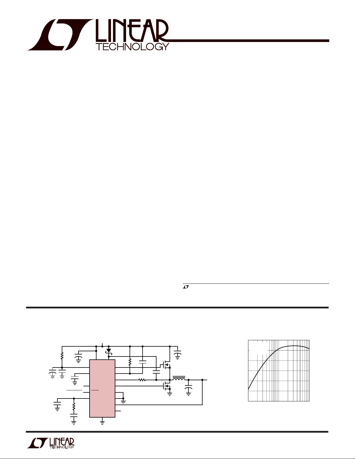
4.7µF
U
O
A
PPLICATITYPICAL
TA = 25°C
= 5V
PV
CC
V
= 3.3V
OUT
Efficiency
LOAD CURRENT (A)
10
1430 TA02
Typical 5V to 3.3V, 10A Application
5V
+
C
IN
220µF
×4
Q1A, Q1B
2 IN PARALLEL
2.7µH/15A
+
Q2
C
OUT
330µF
×6
1430 TA01
3.3V
10A
CC2
LTC1430A
SENSE
SENSE
PV
PGND
–
CC1
I
MAX
GND
MBR0530T1
G1
I
FB
G2NC
+
FB NC
16k
0.1µF
1k
Q1A, Q1B, Q2: MOTOROLA MTD20N03HL
: AVX-TPSE227M010R0100
C
IN
: AVX-TPSE337M006R0100
C
OUT
0.1µF
+
0.1µF
SHUTDOWN
R
7.5k
0.01µF
C
C
C
4700pF
1µF
PV
V
CC
SS
FREQSET
SHDN
COMP
100Ω
+
C1
220pF
100
90
80
70
EFFICIENCY (%)
60
50
40
0.1 1
1
Page 2
LTC1430A
A
W
O
LUTEXI TIS
S
A
WUW
U
ARB
G
Supply Voltage
VCC....................................................................... 9V
PV
.............................................................. 13V
CC1, 2
Input Voltage
IFB......................................................... –0.3V to 18V
All Other Inputs ...................... –0.3V to (VCC + 0.3V)
WU
/
PACKAGE
G1
PV
CC1
GND
FB
T
JMAX
O
RDER I FOR ATIO
TOP VIEW
1
2
3
4
S8 PACKAGE
8-LEAD PLASTIC SO
= 150°C, θJA = 150°C/W
ORDER
PART NUMBER
G2
8
/PV
V
7
CC
CC2
COMP
6
SHDN
5
LTC1430ACS8
S8 PART MARKING
1430A
(Note 1)
Junction Temperature........................................... 150°C
Operating Temperature Range
LTC1430AC ............................................. 0°C to 70°C
LTC1430AI ........................................ – 40°C to 85°C
Storage Temperature Range ................ –65°C to 150°C
Lead Temperature (Soldering, 10 sec)................. 300°C
U
TOP VIEW
1
G1
2
PV
CC1
3
PGND
4
GND
–
SENSE
SENSE
16-LEAD PLASTIC SSOP
5
6
FB
+
7
8
SHDN
GN PACKAGE
T
= 150°C, θJA = 130°C/W (GN)
JMAX
T
= 150°C, θJA = 110°C/W (S)
JMAX
G2
16
PV
15
CC2
V
14
CC
I
13
FB
I
12
MAX
FREQSET
11
COMP
10
SS
9
S PACKAGE
16-LEAD PLASTIC SO
ORDER
PART NUMBER
LTC1430ACGN
LTC1430AIGN
LTC1430ACS
Consult factory for Military grade parts.
ELECTRICAL CHARACTERISTICS
VCC = 5V, T
SYMBOL PARAMETER CONDITIONS MIN TYP MAX MIN TYP MAX UNITS
V
CC
PV
CC
V
OUT
V
FB
∆V
OUT
I
VCC
I
PVCC
f
OSC
= 25°C (Note 2) unless otherwise noted.
A
LTC1430AC LTC1430AI
Supply Voltage ● 4848V
PV
, PV
CC1
Output Voltage Figure 1 3.30 3.30 V
Feedback Voltage SENSE+ and SENSE– Floating , ● 1.25 1.265 1.28 1.23 1.265 1.29 V
Output Load Regulation Figure 1, I
Output Line Regulation Figure 1, V
Supply Current (VCC Only) Figure 2, V
Supply Current (PVCC) Figure 2, PVCC = 5V, V
Internal Oscillator Frequency FREQSET Floating ● 140 200 260 130 200 300 kHz
Voltage ● 313313V
CC2
= 2.5V
V
COMP
= 0A to 10A 5 5 mV
OUT
= 4.75V to 5.25V 1 1 mV
CC
= V
SHDN
V
= 0V 1 10 1 10 µA
SHDN
V
= 0V 0.1 0.1 µA
SHDN
CC
= VCC (Note 3) 1.5 1.5 mA
SHDN
● 350 700 350 700 µA
2
Page 3
LTC1430A
ELECTRICAL CHARACTERISTICS
VCC = 5V, T
SYMBOL PARAMETER CONDITIONS MIN TYP MAX MIN TYP MAX UNITS
V
IH
V
IL
I
IN
g
mV
g
mI
A
V
I
MAX
I
SS
tr, t
s
t
NOV
DC
MAX
= 25°C (Note 2) unless otherwise noted.
A
LTC1430AC LTC1430AI
SHDN Input High Voltage ● 2.4 2.4 V
SHDN Input Low Voltage ● 0.8 0.8 V
SHDN Input Current ● ±0.1 ±1 ±0.1 ±1 µA
Error Amplifier Transconductance ● 350 650 1100 300 650 1200 µmho
I
Amplifier Transconductance (Note 4) 2400 2400 µmho
LIM
Error Amplifier Open-Loop Gain (Note 5) ● 40 48 40 48 dB
I
Sink Current V
MAX
I(MAX)
= V
CC
● 8 12 16 8 12 17 µA
Soft Start Source Current VSS = 0V ● –8 –12 –16 –8 –12 –17 µA
Driver Rise/Fall Time Figure 3, PV
Driver Non-Overlap Time Figure 3, PV
Maximum Duty Cycle Figure 3, V
= 1.265V
V
FB
= PV
CC1
CC1
COMP
= 5V 80 250 80 250 ns
CC2
= PV
= 5V 25 130 250 25 130 250 ns
CC2
= VCC, ● 90 93.5 89 93.5 %
The ● denotes specifications which apply over the full operating
temperature range.
Note 1: Absolute Maximum Ratings are those values beyond which the life
of a device may be impaired.
Note 2: All currents into device pins are positive; all currents out of device
pins are negative. All voltages are referenced to ground unless otherwise
specified.
Note 3: Supply current in normal operation is dominated by the current
needed to charge and discharge the external FET gates. This will vary with
the LTC1430A operating frequency, operating voltage and the external
FETs used.
Note 4: The I
normal (not current limited) operation, the I
Note 5: The open-loop DC gain and transconductance from the FB pin
(SENSE
amplifier can sink but cannot source current. Under
LIM
+
and SENSE– floating) to COMP pin will be AV and gm
output current will be zero.
LIM
V
respectively.
3
Page 4
LTC1430A
TEMPERATURE (°C)
–40
70
DUTY CYCLE (%)
75
85
90
95
0
40
60
1430 G03
80
–20 20
80
100
100
V
COMP
= V
CC
VFB = 1.265V
LOAD CURRENT (A)
0
–1.0
∆V
OUT
(mV)
–0.8
–0.4
–0.2
0
0.4
1
5
7
1460 G06
–0.6
0.2
4
9
10
2
3
68
TA = 25°C
V
OUT
= 3.3V
V
CC
= 5V
FIGURE 4
UW
TYPICAL PERFOR A CE CHARACTERISTICS
I
Pin Sink Current
MAX
vs Temperature
14.0
VCC = 5V
13.5
Oscillator Frequency
vs Temperature
240
VCC = 5V
FREQSET FLOATING
230
Maximum Duty Cycle
vs Temperature
13.0
12.5
12.0
CURRENT (µA)
MAX
I
11.5
11.0
10.5
–40
–20 0
TEMPERATURE (°C)
40 80 100
20 60
Error Amplifier Transconductance
vs Temperature
850
800
750
700
650
600
550
500
450
TRANSCONDUCTANCE (µmho)
400
350
gm =
–20 20
–40
∆I
COMP
∆V
FB
0
TEMPERATURE (°C)
40
60 100
1430 G01
80
1430 G04
220
210
200
190
OSCILLATOR FREQUENCY (kHz)
180
170
(mV)
FB
∆V
–10
–40
–20 0
∆V
vs Temperature
FB
10
VCC = 5V
8
6
4
2
0
–2
–4
–6
–8
–20 0 40
–40
20 60
TEMPERATURE (°C)
20
TEMPERATURE (°C)
40 80 100
1430 G02
Load Regulation
60 80 100
1430 G05
4
OUTPUT VOLTAGE (V)
Output Voltage vs Load Current
with Current Limit
4.0
3.5
3.0
2.5
2.0
1.5
1.0
0.5
R
= 10k R
I(MAX)
TA = 25°C
= 5V
V
CC
FIGURE 4
0
24 8
0
LOAD CURRENT (A)
= 16k
I(MAX)
6
Supply Current
vs Oscillator Frequency
1000
TA = 25°C
= 5V
V
CC
FIGURE 4
100
10
SUPPLY CURRENT (mA)
1
12
10
1430 G07
0.1
0 200 300 400
100
OSCILLATOR FREQUENCY (kHz)
IV
CC
IPVCC (LOADED
WITH 10,000pF,
= 12V)
PV
CC
(NO LOAD,
IPV
CC
= 12V)
PV
CC
IPVCC (NO LOAD,
= 5V)
PV
CC
500
1430 G08
Page 5

UU U
PI FU CTIO S
LTC1430A
(16-Lead Package/8-Lead Package)
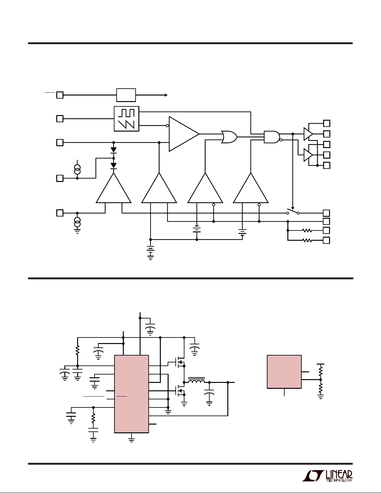
G1 (Pin 1/Pin 1): Driver Output 1. Connect this pin to the
gate of the upper N-channel MOSFET, Q1. This output will
swing from PV
to PGND. It will always be low when G2
CC1
is high.
PV
(Pin 2/Pin 2): Power VCC for Driver 1. This is the
CC1
power supply input for G1. G1 will swing from PGND to
PV
. PV
CC1
PVCC + V
must be connected to a potential of at least
CC1
(Q1). This potential can be generated using
GS(ON)
an external supply or a simple charge pump connected to
the switching node between the upper MOSFET and the
lower MOSFET; see Applications Information for details.
PGND (Pin 3/Pin 3): Power Ground. Both drivers return to
this pin. It should be connected to a low impedance ground
in close proximity to the source of Q2. 8-lead parts have
PGND and GND tied together at Pin 3.
GND (Pin 4/Pin 3): Signal Ground. All low power internal
circuitry returns to this pin. To minimize regulation errors
due to ground currents, GND should be connected to
PGND right at the LTC1430A. 8-lead parts have PGND and
GND tied together internally at Pin 3.
SENSE–, FB, SENSE+ (Pins 5, 6, 7/Pin 4): These three
pins connect to the internal resistor divider and to the
internal feedback node. To use the internal divider to set
the output voltage to 3.3V, connect SENSE+ to the positive
terminal of the output capacitor and SENSE– to GND. FB
should be left floating in applications that use the internal
divider. To use an external resistor divider to set the output
voltage, float SENSE+ and SENSE– and connect the external resistor divider to FB.
COMP (Pin 10/Pin 6): External Compensation. The COMP
pin is connected directly to the output of the error amplifier
and the input of the PWM. An RC network is used at this
node to compensate the feedback loop to provide optimum transient response. See Applications Information for
compensation details.
FREQSET (Pin 11/NA): Frequency Set. This pin is used to
set the free running frequency of the internal oscillator.
With the pin floating, the oscillator runs at about 200kHz.
A resistor from FREQSET to ground will speed up the
oscillator; a resistor to VCC will slow it down. See Applications Information for resistor selection details.
I
(Pin 12/NA): Current Limit Set. I
MAX
sets the thresh-
MAX
old for the internal current limit comparator. If IFB drops
below I
limit. I
with G1 on, the LTC1430A will go into current
MAX
has a 12µA pull-down to GND. It can be adjusted
MAX
with an external resistor to PVCC or an external voltage
source.
IFB (Pin 13/NA): Current Limit Sense. Connect to the
switched node at the source of Q1 and the drain of Q2
through a 1k resistor. The 1k resistor is required to prevent
voltage transients from damaging IFB. This pin can be
taken up to 18V above GND without damage.
VCC (Pin 14/Pin 7): Power Supply. All low power internal
circuits draw their supply from this pin. Connect to a clean
power supply, separate from the main PVCC supply at the
drain of Q1. This pin requires a 4.7µF or greater bypass
capacitor. 8-lead parts have VCC and PV
tied together
CC2
at Pin 7 and require at least a 10µF bypass to GND.
SHDN (Pin 8/Pin 5): Shutdown. A TTL compatible low
level at SHDN for longer than 50µs puts the LTC1430A into
shutdown mode. In shutdown, G1 and G2 go low, all
internal circuits are disabled and the quiescent current
drops to 10µA max. A TTL compatible high level at SHDN
allows the part to operate normally.
SS (Pin 9/NA): Soft Start. The SS pin allows an external
capacitor to be connected to implement a soft start function. An external capacitor from SS to ground controls the
start-up time and also compensates the current limit loop,
allowing the LTC1430A to enter and exit current limit
cleanly. See Applications Information for more details.
PV
(Pin 15/Pin 7): Power VCC for Driver 2. This is the
CC2
power supply input for G2. G2 will swing from GND to
PV
. PV
CC2
supply. 8-lead parts have VCC and PV
is usually connected to the main high power
CC2
tied together at
CC2
Pin 7 and require at least a 10µF bypass to GND.
G2 (Pin 16/Pin 8): Driver Output 2. Connect this pin to the
gate of the lower N-channel MOSFET, Q2. This output will
swing from PV
to PGND. It will always be low when G1
CC2
is high.
5
Page 6
LTC1430A
–
+
–
+
I
LIM
FB MIN
PWM
MAX
+
40mV
20k
+
1.265V
12µA
+
40mV
12µA
12.4k
PV
CC1
SHDN
FREQSET
COMP
SS
I
MAX
V
CC
PV
CC2
G1
G2
PGND
I
FB
FB
SENSE
+
SENSE
–
1430 BD
INTERNAL
SHUTDOWN
50µs
DELAY
BLOCK DIAGRAM
W
TEST CIRCUITS
4.7µF
6
= 12V
PV
CC1
PV
CC2
= 5V
+
0.01µF
R
C
7.5k
C
4700pF
1µF
PV
CC2
V
CC
SS
LTC1430A
FREQSET
SHDN
COMP
C
SENSE
100Ω
+
C1
220pF
0.1µF
SHUTDOWN
PV
CC1
I
MAX
PGND
GND
SENSE
–
+
1µF
G1
I
FB
G2NC
+
FB NC
+
C
IN
220µF
×4
Q1A, Q1B
2 IN PARALLEL
2.7µH/15A
+
Q2
Q1A, Q1B, Q2: MOTOROLA MTD20N03HL
C
: AVX-TPSE227M010R0100
IN
C
: AVX-TPSE337M006R0100
OUT
Figure 1
C
OUT
330µF
×6
3.3V
LTC1430A
SENSE
FB MEASUREMENT
+
SENSE
FB
–
NC
NC
V
OUT
1430 F01
1.61k
1k
Page 7
TEST CIRCUITS
V
SHDN
SHDN
NC
NC
NC
NC
I
MAX
FREQSET
COMP
SS
GND PGND SENSE
V
CC
V
CCPVCC2
LTC1430A
PV
SENSE
PV
CC
CC1IFB
–
LTC1430A
5V
+
10µF
PV
PV
V
CC1
CC
V
G1
G2
FB
NC
NC
NC
+
COMP
COMP
LTC1430A
V
FB
FB
GND
CC2
PGND
G1
10,000pF
G2
10,000pF
0.1µF
G1 RISE/FALL
G2 RISE/FALL
4.7µF
+
Figure 2
100Ω
0.1µF
SHUTDOWN
C1
220pF
+
0.01µF
R
C
7.5k
C
4700pF
1430 F02
1430 F03
Figure 3
V
CC
PV
CC1
I
MAX
PGND
GND
SENSE
–
1N4148
G1
I
FB
G2NC
+
FB NC
0.1µF
16k
1k
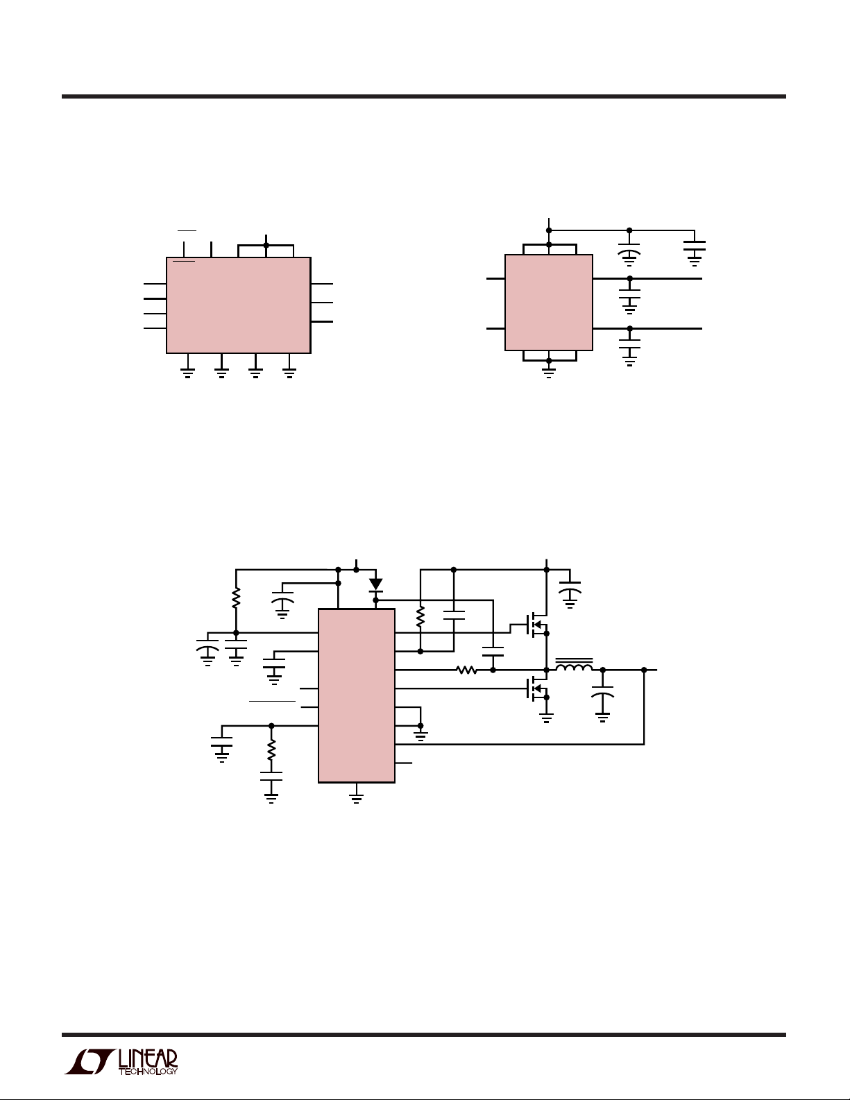
Q1A, Q1B, Q2: MOTOROLA MTD20N03HL
: AVX-TPSE227M010R0100
C
IN
C
: AVX-TPSE337M006R0100
OUT
1µF
PV
CC2
V
CC
SS
LTC1430A
FREQSET
SHDN
COMP
C
SENSE
0.1µF
V
= 5V
IN
Q1A, Q1B
2 IN PARALLEL
2.7µH/15A
Q2
+
C
IN
220µF
×4
+
C
OUT
330µF
×6
3.3V
1430 F04
Figure 4
7
Page 8

LTC1430A
U
WUU
APPLICATIONS INFORMATION
OVERVIEW
T
he LTC1430A is a voltage feedback PWM switching
regulator controller (see Block Diagram) designed for use
in high power, low voltage step-down (buck) converters.
It includes an onboard PWM generator, a precision reference trimmed to ±0.5%, two high power MOSFET gate
drivers and all necessary feedback and control circuitry to
form a complete switching regulator circuit. The PWM
loop nominally runs at 200kHz.
The 16-lead versions of the LTC1430A include a current
limit sensing circuit that uses the upper external power
MOSFET as a current sensing element, eliminating the
need for an external sense resistor.
Also included in the 16-lead version is an internal soft start
feature that requires only a single external capacitor to
operate. In addition, 16-lead parts feature an adjustable
oscillator which can run at frequencies from 50kHz to
500kHz, allowing added flexibility in external component
selection. The 8-lead version does not include current
limit, internal soft start or frequency adjustability.
THEORY OF OPERATION
Primary Feedback Loop
The LTC1430A senses the output voltage of the circuit at
the output capacitor with the SENSE+ and SENSE– pins
and feeds this voltage back to the internal transconductance amplifier FB. FB compares the resistor-divided output voltage to the internal 1.265V reference and outputs an
error signal to the PWM comparator. This is then compared to a fixed frequency sawtooth waveform generated
by the internal oscillator to generate a pulse width modulated signal. This PWM signal is fed back to the external
MOSFETs through G1 and G2, closing the loop. Loop
compensation is achieved with an external compensation
network at COMP, the output node of the FB transconductance amplifier.
MIN, MAX Feedback Loops
Two additional comparators in the feedback loop provide
high speed fault correction in situations where the FB
amplifier may not respond quickly enough. MIN compares
the feedback signal to a voltage 40mV (3%) below the
internal reference. At this point, the MIN comparator
overrides the FB amplifier and forces the loop to full duty
cycle, set by the internal oscillator at about 93.5%. Similarly, the MAX comparator monitors the output voltage at
3% above the internal reference and forces the output to
0% duty cycle when tripped. These two comparators
prevent extreme output perturbations with fast output
transients, while allowing the main feedback loop to be
optimally compensated for stability.
Current Limit Loop
The 16-lead LTC1430A devices include yet another feedback loop to control operation in current limit. The current
limit loop is disabled in the 8-lead device. The I
fier monitors the voltage drop across external MOSFET Q1
with the IFB pin during the portion of the cycle when G1 is
high. It compares this voltage to the voltage at the I
As the peak current rises, the drop across Q1 due to its
R
that Q1’s drain current has exceeded the maximum level,
I
LIM
capacitor, cutting the duty cycle and controlling the output
current level. At the same time, the I
generates a signal to disable the MIN comparator to
prevent it from conflicting with the current limit circuit. If
the internal feedback node drops below about 0.8V, indicating a severe output overload, the circuitry will force the
internal oscillator to slow down by a factor of as much as
100. If desired, the turn on time of the current limit loop
can be controlled by adjusting the size of the soft start
capacitor, allowing the LTC1430A to withstand short
overcurrent conditions without limiting.
By using the R
the current limit circuit eliminates the sense resistor that
would otherwise be required and minimizes the number of
components in the external high current path. Because
power MOSFET R
with temperature, the LTC1430A current limit is not designed to be accurate; it is meant to prevent damage to the
power supply circuitry during fault conditions. The actual
current level where the limiting circuit begins to take effect
may vary from unit to unit, depending on the power
MOSFETs used. See Soft Start and Current Limit for more
details on current limit operation.
increases. When IFB drops below I
DS(ON)
starts to pull current out of the external soft start
of Q1 to measure the output current,
DS(ON)
is not tightly controlled and varies
DS(ON)
MAX
LIM
ampli-
LIM
pin.
MAX
, indicating
comparator
8
Page 9

LTC1430A
U
WUU
APPLICATIONS INFORMATION
MOSFET Gate Drive
Gate drive for the top N-channel MOSFET Q1 is supplied
from PV
power supply input) by at least one power MOSFET
V
GS(ON)
allows PV
up to 13V maximum. This higher voltage can be supplied
with a separate supply, or it can be generated using a
simple charge pump as shown in Figure 5. When using a
separate PV
inrush current if PV
93.5% maximum duty cycle ensures that the charge pump
will always provide sufficient gate drive to Q1. Gate drive
for the bottom MOSFET Q2 is provided through PV
16-lead devices or VCC/PV
can usually be driven directly from PVCC with 16-lead
parts, although it can also be charge pumped or connected
to an alternate supply if desired. 3.3V input applications
use 3.3V at PVCC and 5V at VCC and PV
Supply Operation for more details. The 8-lead part
requires an RC filter from PVCC to VCC to ensure proper
operation; see Input Supply Considerations.
. This supply must be above PVCC ( the main
CC1
for efficient operation. An internal level shifter
to operate at voltages above VCC and PVCC,
CC1
supply, the PVCC input may exhibit a large
CC1
is present during power up. The
CC1
for
CC2
for the 8-lead device. PV
CC2
. See 3.3V Input
CC1
CC2
V
IN
CONTROLLER
Figure 6a. Classical Buck Architecture
CONTROLLER
Figure 6b. Synchronous Buck Architecture
Q1
V
OUT
D1
1430 F06a
V
IN
Q1
V
OUT
Q2
1430 F06b
much lower than the VF of the diode in the classical circuit.
This more than offsets the additional gate drive required
by the second MOSFET, allowing the LTC1430A to achieve
efficiencies in the mid-90% range for a wide range of load
currents.
PV
CC
OPTIONAL
USE FOR PV
D
Z
12V
1N5242
≥ 7V
CC
PV
CC2
LTC1430A
Figure 5. Doubling Charge Pump
MBR0530T1
PV
CC1
0.1µF
G1
G2
Q1
L1
V
OUT
Q2
+
C
OUT
1430 F05
Synchronous Operation
The LTC1430A uses a synchronous switching architecture, with MOSFET Q2 taking the place of the diode in a
classical buck circuit (Figure 6). This improves efficiency
by reducing the voltage drop and the resultant power
dissipation across Q2 to VON = (I)(R
DSON(Q2)
), usually
Another feature of the synchronous architecture is that
unlike a diode, Q2 can conduct current in either direction.
This allows the output of a typical LTC1430A circuit to sink
current as well as sourcing it while remaining in regulation. The ability to sink current at the output allows the
LTC1430A to be used with reactive or other nonconventional
loads that may supply current to the regulator as well as
drawing current from it. An example is a high current logic
termination supply, such as the GTL terminator shown in
the Typical Applications section.
EXTERNAL COMPONENT SELECTION
Power MOSFETs
Two N-channel power MOSFETs are required for most
LTC1430A circuits. These should be selected based primarily on threshold and on-resistance considerations;
thermal dissipation is often a secondary concern in high
efficiency designs. Required MOSFET threshold should be
determined based on the available power supply voltages
and/or the complexity of the gate drive charge pump
9
Page 10

LTC1430A
DC (Q2) = 1 –
V
OUT
V
IN
=
(V
IN
– V
OUT
)
V
IN
PPLICATI
A
U
O
S
I FOR ATIO
WU
U
scheme. In 5V input designs where an auxiliary 12V supply
is available to power PV
with R
specified at VGS = 5V or 6V can be used with
DS(ON)
CC1
and PV
, standard MOSFETs
CC2
good results. The current drawn from this supply varies
with the MOSFETs used and the LTC1430A’s operating
frequency, but is generally less than 50mA.
LTC1430A designs that use a doubler charge pump to
generate gate drive for Q1 and run from PVCC voltages
below 7V cannot provide enough gate drive voltage to fully
enhance standard power MOSFETs. When run from 5V, a
doubler circuit may work with standard MOSFETs, but the
MOSFET RON may be quite high, raising the dissipation in
the FETs and costing efficiency. Logic level FETs are a
better choice for 5V PVCC systems; they can be fully
enhanced with a doubler charge pump and will operate at
maximum efficiency. Doubler designs running from PV
CC
voltages near 4V will begin to run into efficiency problems
even with logic level FETs; such designs should be built
with tripler charge pumps (see Figure 7) or with newer,
super low threshold MOSFETs. Note that doubler charge
pump designs running from more than 7V and all tripler
charge pump designs should include a zener clamp diode
DZ at PV
to prevent transients from exceeding the
CC1
absolute maximum rating at that pin.
Once the threshold voltage has been selected, RON should
be chosen based on input and output voltage, allowable
power dissipation and maximum required output current.
In a typical LTC1430A buck converter circuit operating in
continuous mode, the average inductor current is equal to
D
12V
1N5242
1N5817
Z
1N5817
1N5817
PV
CC
the output load current. This current is always flowing
through either Q1 or Q2 with the power dissipation split up
according to the duty cycle:
V
DC (Q1) =
OUT
V
IN
The RON required for a given conduction loss can now be
calculated by rearranging the relation P = I2R:
(Q1)
P
RON (Q1) =
RON (Q2) =
P
should be calculated based primarily on required
MAX
DC(Q1)(I
VIN(P
=
V
OUT(IMAX
P
DC(Q2)(I
VIN(P
=
(V
IN
MAX
MAX
MAX
– V
MAX
)(Q1)
(Q2)
MAX
MAX
OUT
2
)
2
)
2
)
)(Q2)
)(I
MAX
2
)
efficiency. A typical high efficiency circuit designed for 5V
in, 3.3V at 10A out might require no more than 3%
efficiency loss at full load for each MOSFET. Assuming
roughly 90% efficiency at this current level, this gives a
P
value of (3.3V)(10A/0.9)(0.03) = 1.1W per FET and
MAX
a required RON of:
10
10µF
LTC1430A
PV
PV
CC2
CC1
Figure 7. Tripling Charge Pump
0.1µF
G1
G2
0.1µF
RON (Q1) = = 0.017Ω
Q1
L1
V
OUT
+
Q2
C
OUT
RON (Q2) = = 0.032Ω
(5V)(1.1W)
2
(3.3V)(10A
)
(5V)(1.1W)
(5V – 3.3V)(10A
2
)
Note that the required RON for Q2 is roughly twice that of
1430 • F07
Q1 in this example. This application might specify a single
0.03Ω device for Q2 and parallel two more of the same
devices to form Q1. Note also that while the required R
ON
values suggest large MOSFETs, the dissipation numbers
Page 11

LTC1430A
∆I = DC
(V
IN – VOUT
)
(f
OSC
)(L)
DC =
V
OUT
V
IN
U
O
PPLICATI
A
are only 1.1W per device or less — large TO-220 packages
and heat sinks are not necessarily required in high efficiency applications. Siliconix Si4410DY (in SO-8) and
Motorola MTD20N03HL (in DPAK) are two small, surface
mount devices with RON values of 0.03Ω or below with 5V
of gate drive; both work well in LTC1430A circuits with up
to 10A output current. A higher P
decrease MOSFET cost and circuit efficiency and increase
MOSFET heat sink requirements.
Inductor
The inductor is often the largest component in an LTC1430A
design and should be chosen carefully. Inductor value and
type should be chosen based on output slew rate requirements and expected peak current. Inductor value is primarily controlled by the required current slew rate. The
maximum rate of rise of the current in the inductor is set
by its value, the input-to-output voltage differential and the
maximum duty cycle of the LTC1430A. In a typical 5V to
3.3V application, the maximum rise time will be:
– V
(V
90% =
IN
L
OUT
S
I FOR ATIO
)
AMPS
SECOND
WU
value will generally
MAX
1.53AµsI
L
U
f
= LTC1430A oscillator frequency
OSC
L = inductor value
Solving this equation with our typical 5V to 3.3V application, we get:
(1.7)(0.66)
(200kHz)(2µH)
Peak inductor current at 10A load:
2.8A
2
The inductor core must be adequate to withstand this peak
current without saturating, and the copper resistance in
the winding should be kept as low as possible to minimize
resistive power loss. Note that the current may rise above
this maximum level in circuits under current limit or under
fault conditions in unlimited circuits; the inductor should
be sized to withstand this additional current.
= 11.4A10A +
= 2.8A
P–P
where L is the inductor value in µH. A 2µH inductor would
have a 0.76A/µs rise time in this application, resulting in a
6.5µs delay in responding to a 5A load current step. During
this 6.5µs, the difference between the inductor current and
the output current must be made up by the output capacitor, causing a temporary droop at the output. To minimize
this effect, the inductor value should usually be in the 1µH
to 5µH range for most typical 5V to 2.xV-3.xV LTC1430A
circuits. Different combinations of input and output voltages and expected loads may require different values.
Once the required value is known, the inductor core type
can be chosen based on peak current and efficiency
requirements. Peak current in the inductor will be equal to
the maximum output load current added to half the peakto- peak inductor ripple current. Ripple current is set by the
inductor value, the input and output voltage and the
operating frequency. If the efficiency is high and can be
approximately equal to 1, the ripple current is approximately equal to:
Input and Output Capacitors
A typical LTC1430A design puts significant demands on
both the input and output capacitors. Under normal steady
load operation, a buck converter like the LTC1430A draws
square waves of current from the input supply at the
switching frequency, with the peak value equal to the
output current and the minimum value near zero. Most of
this current must come from the input bypass capacitor,
since few raw supplies can provide the current slew rate to
feed such a load directly. The resulting RMS current flow
in the input capacitor will heat it up, causing premature
capacitor failure in extreme cases. Maximum RMS current
occurs with 50% PWM duty cycle, giving an RMS current
value equal to I
adequate ripple current rating must be used to ensure
reliable operation. Note that capacitor manufacturers’
ripple current ratings are often based on only 2000 hours
(3 months) lifetime; further derating of the input capacitor
ripple current beyond the manufacturer’s specification is
recommended to extend the useful life of the circuit.
/2. A low ESR input capacitor with an
OUT
11
Page 12

LTC1430A
INTERNAL
CIRCUITRY
V
CC
/PV
CC2
LTC1430A (8-LEAD)
PV
CC1
Q1
L1
Q2
G1
G2
PV
CC
C
OUT
V
OUT
1430 F09
+
INTERNAL
CIRCUITRY
V
CC
LTC1430A (16-LEAD)
PV
CC2
PV
CC1
Q1
L1
Q2
G1
G2
PV
CC
C
OUT
V
OUT
1430 F08
+
PPLICATI
A
The output capacitor in a buck converter sees much less
ripple current under steady-state conditions than the input
capacitor. Peak-to-peak current is equal to that in the
inductor, usually a fraction of the total load current. Output
capacitor duty places a premium not on power dissipation
but on low ESR. During an output load transient, the
output capacitor must supply all of the additional load
current demanded by the load until the LTC1430A can
adjust the inductor current to the new value. ESR in the
output capacitor results in a step in the output voltage
equal to the ESR value multiplied by the change in load
current. A 5A load step with a 0.05Ω ESR output capacitor
will result in a 250mV output voltage shift; this is a 7.6%
output voltage shift for a 3.3V supply! Because of the
strong relationship between output capacitor ESR and
output load transient response, the output capacitor is
usually chosen for ESR, not for capacitance value; a
capacitor with suitable ESR will usually have a larger
capacitance value than is needed to control steady-state
output ripple.
Electrolytic capacitors rated for use in switching power
supplies with specified ripple current ratings and ESR can
be used effectively in LTC1430A applications. OS-CON
electrolytic capacitors from Sanyo give excellent performance and have a very high performance/size ratio for an
electrolytic capacitor. Surface mount applications can use
either electrolytic or dry tantalum capacitors. Tantalum
capacitors must be surge tested and specified for use in
switching power supplies; low cost, generic tantalums are
known to have very short lives followed by explosive
deaths in switching power supply applications. AVX TPS
series surface mount devices are popular tantalum capacitors that work well in LTC1430A applications. A common
way to lower ESR and raise ripple current capability is to
parallel several capacitors. A typical LTC1430A application might require an input capacitor with a 5A ripple
current capacity and 2% output shift with a 10A output
load step, which requires a 0.007Ω output capacitor ESR.
Sanyo OS-CON part number 10SA220M (220µF/10V)
capacitors feature 2.3A allowable ripple current at 85°C
and 0.035Ω ESR; three in parallel at the input and six at the
output will meet the above requirements.
12
U
O
S
I FOR ATIO
WU
U
Input Supply Considerations/Charge Pump
The 16-lead LTC1430A requires four supply voltages to
operate: PVCC for the main power input, PV
CC1
and PV
CC2
for MOSFET gate drive and a clean, low ripple VCC for the
LTC1430A internal circuitry (Figure 8). In many applications, PVCC and PV
can be tied together and fed from a
CC2
common high power supply, provided that the supply
voltage is high enough to fully enhance the gate of external
MOSFET Q2. This can be the 5V system supply if a logic
level MOSFET is used for Q2. VCC can usually be filtered
with an RC from this same high power supply; the low
quiescent current (typically 350µA) allows the use of
relatively large filter resistors and correspondingly small
filter capacitors. 100Ω and 4.7µF usually provide ad-
equate filtering for VCC.
The 8-lead version of the LTC1430A has the PV
CC2
and V
CC
pins tied together inside the package (Figure 9). This pin,
brought out as VCC/PV
, has the same low ripple re-
CC2
quirements as the 16-lead part, but must also be able to
supply the gate drive current to Q2. This can be obtained
Figure 8. 16-Lead Power Supplies
Figure 9. 8-Lead Power Supplies
Page 13

LTC1430A
PPLICATI
A
U
O
S
I FOR ATIO
WU
U
by using a larger RC filter from the PVCC pin; 22Ω and 10µF
work well here. The 10µF capacitor must be VERY close to
the part (preferably right underneath the unit) or output
regulation may suffer.
For both versions of the LTC1430A, PV
than PVCC by at least one external MOSFET V
must be higher
CC1
GS(ON)
to fully
enhance the gate of Q1. This higher voltage can be
provided with a separate supply (typically 12V) which
should power up after PVCC, or it can be generated with a
simple charge pump (Figure 5). The charge pump consists
of a Schottky diode from PVCC to PV
capacitor from PV
to the switching node at the drain of
CC1
Q2. This circuit provides 2PVCC – VF to PV
and a 0.1µF
CC1
while Q1 is
CC1
ON and PVCC – VF while Q1 is OFF where VF is the ON
voltage of the Schottky diode. Ringing at the drain of Q2
can cause transients above 2PVCC at PV
; if PVCC is
CC1
higher than 7V, a 12V zener diode should be included from
PV
to PGND to prevent transients from damaging the
CC1
circuitry at PV
or the gate of Q1.
CC2
More complex charge pumps can be constructed with the
16-lead versions of the LTC1430A to provide additional
voltages for use with standard threshold MOSFETs or very
low PVCC voltages. A tripling charge pump (Figure 7) can
provide 2PVCC and 3PVCC voltages. These can be connected to PV
CC2
and PV
respectively, allowing stan-
CC1
dard threshold MOSFETs to be used with 5V at PVCC or 5V
logic level threshold MOSFETs to be used with 3.3V at
PVCC. VCC can be driven from the same potential as PV
CC2
,
allowing the entire system to run from a single 3.3V
supply. Tripling charge pumps require the use of Schottky
diodes to minimize forward drop across the diodes at
start-up. The tripling charge pump circuit will tend to
rectify any ringing at the drain of Q2 and can provide well
more than 3PVCC at PV
; all tripling (or higher multiply-
CC1
ing factor) circuits should include a 12V zener clamp diode
DZ to prevent overvoltage at PV
CC1
.
3.3V Input Supply Operation
The LTC1430A can be used with input supply voltages
lower than 5V as long as a low power 5V supply is available
to power the LTC1430A itself and to provide gate drive to
the external MOSFETs. A typical 3.3V to 2.5V application
is shown in Figure 10. The circuit can supply up to 10A at
2.5V output, and draws this power from the 3.3V supply.
The 5V supply typically needs to supply about 20mA to
provide gate drive to the external MOSFETs and keep the
LTC1430A control circuits powered. For applications where
there is no 5V supply available, see the LTC1649 data
sheet.
Compensation and Transient Response
The LTC1430A voltage feedback loop is compensated at
the COMP pin; this is the output node of the internal g
m
error amplifier. The loop can generally be compensated
4.7µF
1µF
3.3V
Q1A, Q1B
2 IN PARALLEL
2.7µH/15A
Q2
+
C
IN
220µF
×4
2.5V
OUT
976Ω
1%
1k
1%
1430 F10
10A
+
C
330µF
×6
5V
SENSE
NC
PV
PGND
–
CC1
I
MAX
GND
MBR0530T1
G1
I
FB
G2NC
+
FB
16k
NC
Q1A, Q1B, Q2: INTERNATIONAL RECTIFIER IRF7801
: AVX-TPSE227M010R0100
C
IN
: AVX-TPSE337M006R0100
C
OUT
0.1µF
1k
+
0.01µF
R
C
7.5k
C
4700pF
1µF
PV
CC2
V
CC
SS
LTC1430A
FREQSET
SHDN
COMP
SENSE
C
100Ω
+
0.1µF
SHUTDOWN
C1
220pF
Figure 10. 3.3V to 2.5V, 10A Application
13
Page 14

LTC1430A
1430 F12
C
SS
COMP
SS
LTC1430A
12µA
V
CC
FB
PPLICATI
A
U
O
S
I FOR ATIO
WU
U
properly with an RC network from COMP to GND and an
additional small C from COMP to GND (Figure 11). Loop
stability is affected by inductor and output capacitor
values and by other factors. Optimum loop response can
be obtained by using a network analyzer to find the loop
poles and zeros; nearly as effective and a lot easier is to
empirically tweak the RC values until the transient recovery
looks right with an output load step. Table 1 shows
recommended compensation components for 5V to 3.3V
applications based on the inductor and output capacitor
values. The values were calculated using multiple paralleled 330µF AVX TPS series surface mount tantalum
capacitors as the output capacitor.
Table 1. Recommended Compensation Network for 5V to 3.3V
Application Using Multiple 330µF AVX Output Capacitors
L1 (µH) C
1 990 1.8 0.022 820
1 1980 3.6 0.01 470
1 4950 9.1 0.0047 150
1 9900 18 0.0022 82
2.7 990 3.6 0.01 470
2.7 1980 7.5 0.0047 220
2.7 4950 18 0.0022 82
2.7 9900 39 0.001 39
5.6 990 9.1 0.0047 150
5.6 1980 18 0.0022 82
5.6 4950 47 820pF 33
5.6 9900 91 470pF 15
10 990 18 0.0022 82
10 1980 39 0.001 39
10 4950 91 470pF 15
10 9900 180 220pF 10
(µF) RC (kΩ)C
OUT
(µF) C1 (pF)
C
LTC1430A
COMP
R
C
C
GND SGND
Figure 11. Compensation Pin Hook-Up
C1C
1430 F11
and inductor core saturation rating. Minimizing output
capacitor ESR will also help optimize output transient
response. See Input and Output Capacitors for more
information.
Soft Start and Current Limit
The 16-lead versions of the LTC1430A include a soft start
circuit at the SS pin; this circuit is used both for initial startup and during current limit operation. The soft start and
current limit circuitry is disabled in the 8-lead version. SS
requires an external capacitor to GND with the value
determined by the required soft start time. An internal
12µA current source is included to charge the external
capacitor. Soft start functions by clamping the maximum
voltage that the COMP pin can swing to, thereby controlling the duty cycle (Figure 12). The LTC1430A will begin to
operate at low duty cycle as the SS pin rises to about 2V
below VCC. As SS continues to rise, the duty cycle will
increase until the error amplifier takes over and begins to
regulate the output. When SS reaches 1V below VCC the
Output transient response is set by three major factors: the
time constant of the inductor and the output capacitor, the
ESR of the output capacitor, and the loop compensation
components. The first two factors usually have much
more impact on overall transient recovery time than the
third; unless the loop compensation is way off, more
improvement can be had by optimizing the inductor and
the output capacitor than by fiddling with the loop compensation components. In general, a smaller value inductor will improve transient response at the expense of ripple
14
Figure 12. Soft Start Clamps COMP Pin
Page 15

LTC1430A
PPLICATI
A
U
O
S
I FOR ATIO
WU
U
LTC1430A will be in full operation. An internal switch
shorts the SS pin to GND during shutdown.
The LTC1430A detects the output current by watching the
voltage at IFB while Q1 is ON. The I
this voltage to the voltage at I
MAX
amplifier compares
LIM
(Figure 13). In the ON
state, Q1 has a known resistance; by calculating backwards, the voltage generated at IFB by the maximum
output current in Q1 can be determined. As IFB falls below
I
, I
MAX
will begin to sink current from the soft start pin,
LIM
causing the voltage at SS to fall. As SS falls, it will limit the
output duty cycle, limiting the current at the output.
Eventually the system will reach equilibrium, where the
pull-up current at the SS pin matches the pull-down
current in the I
amplifier; the LTC1430A will stay in this
LIM
state until the overcurrent condition disappears. At this
time IFB will rise, I
will stop sinking current and the
LIM
internal pull-up will recharge the soft start capacitor,
restoring normal operation. Note that the IFB pin requires
an external 1k series resistor to prevent voltage transients
at the drain of Q2 from damaging internal structures.
0.1µF
PV
R
IMAX
I
MAX
+
The I
12µA
V
SS
C
SS
Figure 13. Current Limit Operation
amplifier pulls current out of SS in proportion to
LIM
I
LIM
CC
12µA
LTC1430A
the difference between IFB and I
1k
I
FB
–
1430 F13
. Under mild overload
MAX
CC
Q1
Q2
conditions, the SS pin will fall gradually, creating a time
delay before current limit takes effect. Very short, mild
overloads may not trip the current limit circuit at all.
Longer overload conditions will allow the SS pin to reach
a steady level, and the output will remain at a reduced
voltage until the overload is removed. Serious overloads
will generate a larger overdrive at I
, allowing it to pull SS
LIM
down more quickly and preventing damage to the output
components.
The I
amplifier output is disabled when Q1 is OFF to
LIM
prevent the low IFB voltage in this condition from activating
the current limit. It is re-enabled a fixed 170ns after Q1
turns on; this allows for the IFB node to slew back high and
the I
amplifier to settle to the correct value. As the
LIM
LTC1430A goes deeper into current limit, it will reach a
point where the Q1 on-time needs to be cut to below 170ns
to control the output current. This conflicts with the
minimum settling time needed for proper operation of the
I
amplifier. At this point, a secondary current limit
LIM
circuit begins to reduce the internal oscillator frequency,
lengthening the off-time of Q1 while the on-time remains
constant at 170ns. This further reduces the duty cycle,
allowing the LTC1430A to maintain control over the output
current.
Under extreme output overloads or short circuits, the I
LIM
amplifier will pull the SS pin more than 2V below VCC in a
single switching cycle, cutting the duty cycle to zero. At
this point all switching stops, the output current decays
through Q2 and the LTC1430A runs a partial soft start
cycle and restarts. If the short is still present the cycle will
repeat. Peak currents can be quite high in this condition,
but the average current is controlled and a properly
designed circuit can withstand short circuits indefinitely
with only moderate heat rise in the output FETs. In addition, the soft start cycle repeat frequency can drop into the
low kHz range, causing vibrations in the inductor which
provide an audible alarm that something is wrong.
Oscillator Frequency
The LTC1430A includes an onboard current controlled
oscillator which will typically free-run at 200kHz. An
internal 20µA current is summed with any current in or out
of the FREQSET pin (Pin 11), setting the oscillator frequency to approximately 10kHz/µA. FREQSET is internally
servoed to the LTC1430A reference voltage (1.265V).
With FREQSET floating, the oscillator is biased from the
15
Page 16

LTC1430A
U
O
PPLICATI
A
internal 20µA source and runs at 200kHz. Connecting a
50k resistor from FREQSET to ground will sink an additional 25µA from FREQSET, causing the internal oscillator
to run at approximately 450kHz. Sourcing an external
10µA current into FREQSET will cut the internal frequency
to 100kHz. An internal clamp prevents the oscillator from
running slower than about 50kHz. Tying FREQSET to V
will cause it to run at this minimum speed.
Shutdown
The LTC1430A includes a low power shutdown mode,
controlled by the logic at the SHDN pin. A high at SHDN
allows the part to operate normally. A low level at SHDN
stops all internal switching, pulls COMP and SS to ground
internally and turns Q1 and Q2 off. In shutdown, the
LTC1430A itself will drop below 1µA quiescent current
typically, although off-state leakage in the external
MOSFETs may cause the total PVCC current to be somewhat higher, especially at elevated temperatures. When
SHDN rises again, the LTC1430A will rerun a soft start
cycle and resume normal operation. Holding the LTC1430A
in shutdown during PVCC power up removes any PV
sequencing constraints.
External Clock Synchronization
The LTC1430A SHDN pin can double as an external clock
input for applications that require a synchronized clock or
a faster switching speed. The SHDN pin terminates the
internal sawtooth wave and resets the oscillator immediately when it goes low, but waits 50µs before shutting
down the rest of the internal circuitry. A clock signal
applied directly to the SHDN pin will force the LTC1430A
internal oscillator to lock to its frequency as long as the
external clock runs faster than the internal oscillator
frequency. The LTC1430A can be synchronized to frequencies between 250kHz and 350kHz with no additional
components.
The LTC1430A is synchronizable at frequencies from
200kHz to 500kHz. Frequencies above 300kHz can cause
a decrease in the maximum obtainable duty cycle as rise/
fall time and propagation delay take up a large fraction of
the switch cycle. Circuits using these frequencies should
S
I FOR ATIO
WU
U
CC
CC1
be checked carefully in applications where operation near
dropout is important—like 3.3V to 2.5V converters. Frequencies above 500kHz can cause erratic current limit
operation and are not recommended.
LAYOUT CONSIDERATIONS
Grounding
Proper grounding is critical for the LTC1430A to obtain
specified output regulation. Extremely high peak currents
(as high as several amps) can flow between the bypass
capacitors and the PV
currents can generate significant voltage differences between two points that are nominally both “ground.” As a
general rule, GND and PGND should be totally separated
on the layout, and should be brought together at only one
point, right at the LTC1430A GND and PGND pins. This
helps minimize internal ground disturbances in the
LTC1430A by keeping PGND and GND at the same potential, while preventing excessive current flow from disrupting the operation of the circuits connected to GND. The
PGND node should be as compact and low impedance as
possible, with the negative terminals of the input and
output capacitors, the source of Q2, the LTC1430A PGND
node, the output return and the input supply return all
clustered at one point. Figure 14 is a modified schematic
showing the common connections in a proper layout. Note
that at 10A current levels or above, current density in the
PC board itself can become a concern; traces carrying high
currents should be as wide as possible.
Output Voltage Sensing
The 16-lead versions of the LTC1430A provide three pins
for sensing the output voltage: SENSE+, SENSE– and FB.
SENSE+ and SENSE– connect to an internal resistor
divider which is connected to FB. To set the output of the
LTC1430A to 3.3V, connect SENSE+ to the output as near
to the load as practical and connect SENSE– to the
common GND/PGND point. Note that SENSE– is not a true
differential input sense input; it is just the bottom of the
internal divider string. Connecting SENSE– to the ground
near the load will not improve load regulation. For any
other output voltage, the SENSE+ and SENSE– pins should
CC1
, PV
and PGND pins. These
CC2
16
Page 17

LTC1430A
PPLICATI
A
4.7µF
C1
220pF
4700pF
U
O
S
I FOR ATIO
+
35V
C
R
7.5k
C
0.1µF
GND
NC
NC
C
C
SS
0.01µF
GND
WU
100Ω
PV
V
CC
PV
LTC1430A
I
MAX
FREQSET
SENSE
SHDN
COMP
SS
SENSE
PGNDGND
CC2
CC1
U
PGND
G1
I
FB
+
G2
FB
–
1µF
0.1µF
NC
Figure 14. Typical Schematic Showing Layout Considerations
V
SENSE
LTC1430A
SENSE
+
FB
–
1430 F15
NC
NC
OUT
R1
R2
Figure 15. Using External Resistors to Set Output Voltages
be floated and an external resistor string should be connected to FB (Figure 15). As before, connect the top
resistor (R1) to the output as close to the load as practical
and connect the bottom resistor (R2) to the common
GND/PGND point. In both cases, connecting the top of the
resistor divider (either SENSE+ or R1) close to the load can
significantly improve load regulation by compensating for
any drops in PC traces or hookup wires between the
LTC1430A and the load.
Power Component Hook-Up/Heat Sinking
As current levels rise much above 1A, the power components supporting the LTC1430A start to become physically large (relative to the LTC1430A, at least) and can
require special mounting considerations. Input and output
capacitors need to carry high peak currents and must have
low ESR; this mandates that the leads be clipped as short
as possible and PC traces be kept wide and short. The
5V
TOTAL
+
Q1B*
880µF
(220µF
10V ×4)
2.7µH/15A
3.3V
TOTAL
+
1980µF
(330µF
6.3V ×6)
1430 F14
MBR0530T1
Q1A*
Q2*
PGND
* MOTOROLA MTD20N03HL
power inductor will generally be the most massive single
component on the board; it can require a mechanical holddown in addition to the solder on its leads, especially if it
is a surface mount type.
The power MOSFETs used require some care to ensure
proper operation and reliability. Depending on the current
levels and required efficiency, the MOSFETs chosen may
be as large as TO-220s or as small as SO-8s. High
efficiency circuits may be able to avoid heat sinking the
power devices, especially with TO-220 type MOSFETs. As
an example, a 90% efficient converter working at a steady
3.3V/10A output will dissipate only (33W/90%)10% =
3.7W. The power MOSFETs generally account for the
majority of the power lost in the converter; even assuming
that they consume 100% of the power used by the
converter, that’s only 3.7W spread over two or three
devices. A typical SO-8 MOSFET with a RON suitable to
provide 90% efficiency in this design can commonly
dissipate 2W when soldered to an appropriately sized
piece of copper trace on a PC board. Slightly less efficient
or higher output current designs can often get by with
standing a TO-220 MOSFET straight up in an area with
some airflow; such an arrangement can dissipate as much
as 3W without a heat sink. Designs which must work in
high ambient temperatures or which will be routinely
overloaded will generally fare best with a heat sink.
17
Page 18

LTC1430A
U
O
PPLICATI
A
Figure 17 is a synchronous buck regulator designed to
provide a low voltage, very high current output from a 5V
or lower input voltage. The circuit uses two 8-pin
LTC1430ACS8s, operated 180° out of phase from each
other. Each half of the circuit is good for 15A of output
current, giving 30A total. The LT®1006 amplifier forces the
two half circuits to share the load current equally. This
scheme trades a small amount of additional control circuit
complexity for radical reductions in the volume (hence
cost) of the capacitors and inductors required. Advantages of this approach include very low input and output
ripple voltages, higher ripple frequency and extremely fast
transient response.
By incorporating two regulators phased opposite one
another, both the input ripple currents and the output
ripple currents tend to cancel. This permits running much
higher ripple currents in the output inductors than would
be tolerable with a single channel. The overall output ripple
current in a two phase design is approximately 1/2 of a
single channel’s ripple current, allowing the inductor value
of each channel to be 1/2 that of what a single channel
system would require for equal output ripple. Since energy
storage varies as the square of inductor current, and
directly as the inductance, each inductor stores only 1/8th
the energy of a single inductor design. Since there are two
inductors, total energy storage, and therefore inductor
volume, is 1/4th that of a single phase system.
A similar analysis can be done for the input capacitor
requirements. In fact, a two-phase regulator will actually
require less input capacitance than a single channel design
at 1/2 the load current. Figure 16 shows how the ripple
currents tend to cancel one another.
Another significant advantage of the two-phase topology
is radically improved transient response. During a load
transient, each of the two channels runs to maximum (or
minimum) duty cycle. The two ripple current terms now
end up reinforcing one another rather than canceling. The
result is a very high di/dt, hence, very fast transient
recoveries. Once steady state conditions return, the ripple
currents begin to cancel again, providing very low output
ripple voltage.
S
I FOR ATIO
WU
U
A + B
CHANNEL A
CHANNEL B
2µs/DIV
Figure 16. Output Inductor Currents 5A/DIV, 30A Out
The clocking of the two channels is accomplished by the
CD4047, a low cost, CMOS mulitvibrator with a built-in
divide-by-two flip flop. The CD4047 oscillator is set to run
at 600kHz and the Q and Q outputs drive the LTC1430A
shutdown pins. Since the sync signals are derived from
the clock’s divide-by-two outputs, they are inherently
180° out of phase and at the desired 300kHz clock frequency. Q1, D1 and the two resistors connected to Q1’s
base are used to disable the synchronization at turn-on to
prevent start-up problems. As long as the input-output
differential voltage is large enough to turn on Q1, the sync
circuit is disabled and both LTC1430As will free run at
200kHz. Once the output rises above ≈1.5V, the regulators are allowed to lock to the clock.
One challenge with a voltage mode two-phase design is
current sharing. Unlike current mode control which offers
inherent current sharing, voltage mode control virtually
assures that one channel will try to hog a large percentage
of the load current. The circuit gets around this problem
with a current share amplifier. The LT1006 op amp compares the voltage across both sense resistors and adds or
subtracts a small current into the lower LTC1430A’s
feedback divider, forcing it to match the upper LTC1430A’s
current. The two PCB trace resistors are intentionally
chosen to have a very low value to minimize power losses.
The LT1006 features 80µV typical VOS, ensuring reasonably accurate current sharing.
There are three problems associated with this current
sharing approach that must be dealt with. The first is that
1430A F16
18
Page 19

LTC1430A
PPLICATI
A
D1
BAW56CT1
SYNC1
SENSE1
I
CHARGE PUMP
(OPTIONAL)
C23
0.47µF
SYNC2
U
O
S
I FOR ATIO
R24
Q1
MMBT3906LT1
39k
10k
R12
C7
470µF
6.3V
+
R13
TRACE
0.002Ω
C11
470µF
6.3V
+
L2
C5
1µF
0.8µH
Q3
Si4410DY
WU
OUT
V
C18
1000pF
R5
9.76k
1%
C32
470µF
6.3V
+
C10
470µF
6.3V
+
C19
6800pF
R28
1Ω
Q5
Si4410DY
U
C35
C34
1µF
1µF
R17
10k
1%
SENSE2
I
CHARGE PUMP
(OPTIONAL)
C27
C40
1500µF
6.3V
C20
+
C39
+
6800pF
SANYO
1500µF
6.3V
SANYO
1430 F17
R18
10k
1%
OPTIONAL
IN
V
C17
9.76k
470µF
470µF
Q9
1000pF
1%
6.3V
6.3V
Si4410DY
R29
IN
V
1Ω
1µF
C36
C8
470µF
6.3V
+
R11
TRACE
0.002Ω
C12
470µF
6.3V
+
C4
1µF
Q7
Si4410DY
0.47µF
R2
C33
+
C9
+
L1
0.8µH
D2
BAT54
5V
D4
BAT54
R10
10Ω
12V
5V
20k
62k
2.0V
16.9k
16.9k
10k
10k
10k
51k
2.5V
OUT
V
NANANA
NA
3.3V
REF
R24
R17
R18R7R24
IN
V
SUBSTITUTION TABLE
3.3V
43k
39k
36k
C25
R21
1µF
16.9k
10k
6.04k
R17
5V
1Ω
C21
+
16.9k
10k
6.04k
R18
C22
62k
51k
36k
R7
D3
BAT54
Q6
Q2
Si4410DY
1Ω
R20
R1
51Ω
47µF
10V
2
7
1
CC1
PV
CC2
PV
8
1Ω
R22
G1
LTC1430ACS8
G2
C1
1µF
Q4
4
5
FB
SHDN
Si4410DY
(OPTIONAL)
3
GND
COMP
6
C14
C13
R23
1500pF
R14
180pF
R16
R25
10Ω
C24
1Ω
12V 5V
10k
+
C3
25V
22µF
1µF
SYNC1
1k
101113
Q
Q
AST
AST
546
C28
0.1µF
R4
OSC
–T
1k
+T
8123
RET
RCC
CD4047
CX
1
RX
2
C6
5%
NPO
100pF
9
R6
RST
3.09k
5V CLOCK)
(POWER FROM
1%
R3
5V
Si4410DY
1Ω
1Ω
R19
1µF
2
7
1
CC1
PV
CC2
PV
8
C2
Q8
1Ω
R26
4
G1
LTC1430ACS8
G2
5
1µF
SYNC2
12V
Si4410DY
(OPTIONAL)
3
FB
GND
SHDN
COMP
6
R32
10Ω
+
C26
C30
C29
C15
C16
22µF
0.022µF
1µF
R27
1500pF
R15
180pF
25V
1Ω
R8
R30
10k
7
4.3k
1k
SENSE2
I
Figure 17. Low Voltage 30A Power Supply
NOTES:
1. L1 AND L2 ARE PANASONIC ETQP1F0R8LB
2. ALL RESISTORS ±5% UNLESS OTHERWISE MARKED
3. INPUT AND OUTPUT CAPS ARE KEMET T510 SERIES
4. TRACE RESISTORS R11 AND R13 ARE 0.1" WIDE BY 0.675" LONG
R7
51k
6
1
8
SHARE
CURRENT
AMPLIFIER
4
LT1006
+
–
2
3
R9
4.3k
C31
R31
SENSE1
I
0.022µF
C38
1k
3300pF
C37
3300pF
19
Page 20

LTC1430A
PPLICATI
A
U
O
S
I FOR ATIO
WU
U
the sense resistors should be well matched. This is
accomplished by using trace resistors that are laid out
symmetrically. Since they are formed of the same material
and processed identically, they will inherently match very
well. Note that the absolute value of these resistors is not
important; only the match between them is of concern.
The second issue is related to the reference point for the
two sense voltages. In order to avoid the need to use a true
differential amplifier to measure input current, the circuit
is configured such that the input side of these resistors
must be at the exact same potential. If the layout is not
configured this way, the current sharing accuracy will
prove disappointing. With only 0.2Ω sense resistors, a
seemingly small error will produce a rather large current
mismatch between channels.
The last issue is related to having a very noisy sense
voltage. The current waveshape at the input to a buck
regulator is trapezoidal. Therefore, the sense amplifier
must integrate the two current measurements in order that
the average input currents be compared. The two-stage
RC filter on the sense amplifier provides an adequately
clean signal for the share circuit to operate correctly. High
speed is not required in the current sense loop. In balanced
operation any offsets in the slave regulator are dialed out
by the sense amplifier. If a sudden load change should
occur, both regulators will respond immediately and in the
right direction. If there are any gain differences in the two
loops there will need to be a small correction in the current
share error voltage. This can occur over a relatively long
time period with no adverse effects. As such, the share
amplifier’s bandwidth is on the order of a few hundred Hz,
ensuring good noise immunity.
Figure 18 demonstrates the high efficiency achieved with
this two-phase converter. An efficiency > 90% is realized
from a few amperes up to 30A. In theory and in practice,
this multiphase approach can be extended to even higher
current and output power levels. Consult Linear Technology for further details.
100
95
90
85
80
75
70
EFFICIENCY (%)
65
60
55
50
Figure 18. Low Voltage 30A Power Supply Efficiency
5
0
15 20
10
LOAD CURRENT (A)
30
25
1430 F18
20
Page 21

PACKAGEDESCRIPTI
O
U
Dimensions in inches (millimeters) unless otherwise noted.
GN Package
16-Lead Plastic SSOP (Narrow 0.150)
(LTC DWG # 05-08-1641)
0.189 – 0.196*
(4.801 – 4.978)
16
15
14
12 11 10
13
LTC1430A
0.009
(0.229)
9
REF
0.015
± 0.004
(0.38 ± 0.10)
0.007 – 0.0098
(0.178 – 0.249)
0.016 – 0.050
(0.406 – 1.270)
* DIMENSION DOES NOT INCLUDE MOLD FLASH. MOLD FLASH
SHALL NOT EXCEED 0.006" (0.152mm) PER SIDE
** DIMENSION DOES NOT INCLUDE INTERLEAD FLASH. INTERLEAD
FLASH SHALL NOT EXCEED 0.010" (0.254mm) PER SIDE
0° – 8° TYP
× 45°
0.229 – 0.244
(5.817 – 6.198)
0.053 – 0.068
(1.351 – 1.727)
0.008 – 0.012
(0.203 – 0.305)
12
0.150 – 0.157**
(3.810 – 3.988)
5
4
3
678
0.004 – 0.0098
(0.102 – 0.249)
0.025
(0.635)
BSC
GN16 (SSOP) 0398
21
Page 22

LTC1430A
PACKAGEDESCRIPTI
U
O
Dimensions in inches (millimeters) unless otherwise noted.
S8 Package
8-Lead Plastic Small Outline (Narrow 0.150)
(LTC DWG # 05-08-1610)
8
0.189 – 0.197*
(4.801 – 5.004)
7
6
5
0.228 – 0.244
(5.791 – 6.197)
0.010 – 0.020
(0.254 – 0.508)
0.008 – 0.010
(0.203 – 0.254)
*
DIMENSION DOES NOT INCLUDE MOLD FLASH. MOLD FLASH
SHALL NOT EXCEED 0.006" (0.152mm) PER SIDE
**
DIMENSION DOES NOT INCLUDE INTERLEAD FLASH. INTERLEAD
FLASH SHALL NOT EXCEED 0.010" (0.254mm) PER SIDE
× 45°
0°– 8° TYP
0.016 – 0.050
0.406 – 1.270
0.053 – 0.069
(1.346 – 1.752)
0.014 – 0.019
(0.355 – 0.483)
0.150 – 0.157**
(3.810 – 3.988)
1
3
2
4
0.004 – 0.010
(0.101 – 0.254)
0.050
(1.270)
TYP
SO8 0996
22
Page 23

PACKAGEDESCRIPTI
U
O
Dimensions in inches (millimeters) unless otherwise noted.
S Package
16-Lead Plastic Small Outline (Narrow 0.150)
(LTC DWG # 05-08-1610)
16
15
0.386 – 0.394*
(9.804 – 10.008)
13
14
LTC1430A
12
11
10
9
0.010 – 0.020
(0.254 – 0.508)
0.008 – 0.010
(0.203 – 0.254)
*
DIMENSION DOES NOT INCLUDE MOLD FLASH. MOLD FLASH
SHALL NOT EXCEED 0.006" (0.152mm) PER SIDE
**
DIMENSION DOES NOT INCLUDE INTERLEAD FLASH. INTERLEAD
FLASH SHALL NOT EXCEED 0.010" (0.254mm) PER SIDE
×
45
0.016 – 0.050
0.406 – 1.270
°
0° – 8° TYP
0.228 – 0.244
(5.791 – 6.197)
0.053 – 0.069
(1.346 – 1.752)
0.014 – 0.019
(0.355 – 0.483)
0.150 – 0.157**
(3.810 – 3.988)
4
5
0.050
(1.270)
TYP
3
2
1
7
6
8
0.004 – 0.010
(0.101 – 0.254)
S16 0695
Information furnished by Linear Technology Corporation is believed to be accurate and reliable.
However, no responsibility is assumed for its use. Linear Technology Corporation makes no representation that the interconnection of its circuits as described herein will not infringe on existing patent rights.
23
Page 24

LTC1430A
A
PPLICATITYPICAL
R7
C1
15k
0.1µF
R10
3.3kR8130k
C3
220pF
C11
0.068µF
SHDN
C6
0.01µF
C8
22µF
35V
U
O
GTL Terminator
D1
MBR0530T1
C4
+ +
330
6.3V
D1
MBRS340T3
C2
OSCON
R4
51
C7
0.1µF
C10
C16
1µF
15
PV
CC2
14
V
CC
11
FSET
LTC1430A
12
I
MAX
8
SHDN
10
COMP
9
SS
4
SGND
PV
CC1
PGND
–SENSE
+SENSE
2
1
G1
13
I
FB
16
G2
3
5
7
6
FB
R2
3Ω
3Ω
R3
0.1µF
R1
1k
Si4410
Q1
Si4410
L1
2.7µH
680pF
Q2
D2
MBRS340T3
+
R6
10k
R5
16.5k
1%
R9
88.7k
1%
+
C5
330
6.3V
OSCON
C12
330
6.3V
OSCON
C13
330
6.3V
OSCON
+
5V
1.5V OUT
+ +
330
6.3V
TANT
330
6.3V
TANT
ADDITIONAL
DECOUPLING
AT THE LOAD
1430 TA03
RELATED PARTS
PART NUMBER DESCRIPTION COMMENTS
LTC1142 Current Mode Dual Step-Down Switching Regulator Controller Dual Version of LTC1148
LTC1148 Current Mode Step-Down Switching Regulator Controller Synchronous, VIN ≤ 20V
LTC1149 Current Mode Step-Down Switching Regulator Controller Synchronous, VIN ≤ 48V, For Standard Threshold FETs
LTC1159 Current Mode Step-Down Switching Regulator Controller Synchronous, VIN ≤ 40V, For Logic Threshold FETs
LTC1266 Current Mode Step-Up/Down Switching Regulator Controller Synchronous N- or P-Channel FETs, Comparator/
Low-Battery Detector
LTC1267 Current Mode Dual Step-Down Switching Regulator Controller Dual Version of LTC1159
LTC1649 3.3V Input Synchronous Switching Regulator Controller 3.3V Input
1430af, 1430afs LT/TP 0898 4K • PRINTED IN USA
LINEAR TECHNOLOGY CORPORATION 1998
24
Linear Technology Corporation
1630 McCarthy Blvd., Milpitas, CA 95035-7417
(408) 432-1900 ● FAX: (408) 434-0507
●
www.linear-tech.com
 Loading...