

Page 1
FEATURES
LTC1429
Clock-Synchronized
Switched Capacitor
Regulated Voltage Inverter
U
DESCRIPTION
■
Regulated Negative Voltage from a Single
Positive Supply
■
External Clock for Synchronization in Noise
Sensitive Systems
■
REG Output Indicates Output is in Regulation
■
Low Output Ripple: 5mV Typ
■
Can Provide Regulated –5V from a 3V Supply
■
Supply Current: 600µA Typ
■
Shutdown Mode Drops Supply Current to 0.2µA
■
Up to 12mA Output Current
■
Adjustable or Fixed Output Voltages
■
Requires Only Three or Four External Caps
■
Output Regulation: 5%
■
Available in SO-8 Packages
U
APPLICATIONS
■
GaAs FET Bias Generators
■
Negative Supply Generators
■
Battery Powered Systems
■
Single Supply Applications
, LTC and LT are registered trademarks of Linear Technology Corporation.
The LTC®1429 is a switched-capacitor voltage inverter designed to provide a regulated negative voltage from a single
positive supply and permits clock synchronization in noise
sensitive systems. The LTC1429CS operates from a single 3V
to 8V supply and provides an adjustable output voltage from
–1.25V to –8V. An on-chip resistor string allows the
LTC1429CS to be configured for output voltages of –3.5V,
–4V, –4.5V or – 5V. The LTC1429CS8 is optimized for
applications which require a fixed –4V output from a 5V
supply and requires only a single external 0.1µF flying
capacitor. The LTC1429CS requires one or two external
0.1µF capacitors, depending on input voltage. Both versions
require additional external input and output bypass capacitors. An optional compensation capacitor at ADJ/COMP can
be used to reduce the output voltage ripple.
Each version of the LTC1429 guarantees output regulation of
5%. The LTC1429 includes an open-drain REG output which
pulls low when the output is within 5% of the set value. Output
ripple is typically as low as 5mV. The LTC1429 requires an
external clock applied to the SYNC/SD for normal operation
and consumes a typical quiescent current of 600µ A. Holding
the SYNC/SD either high or low brings the device into
shutdown and the supply current drops to 0.2µ A. For applications which don’t have a clock signal available, the LTC1261
provides the same functionality with an internal oscillator. For
applications which require output ripple below 1mV, see the
LTC1550/LTC1551. The LTC1429CS is available in a 14-pin
SO package and the LTC1429CS8 is available in an 8-pin SO
package.
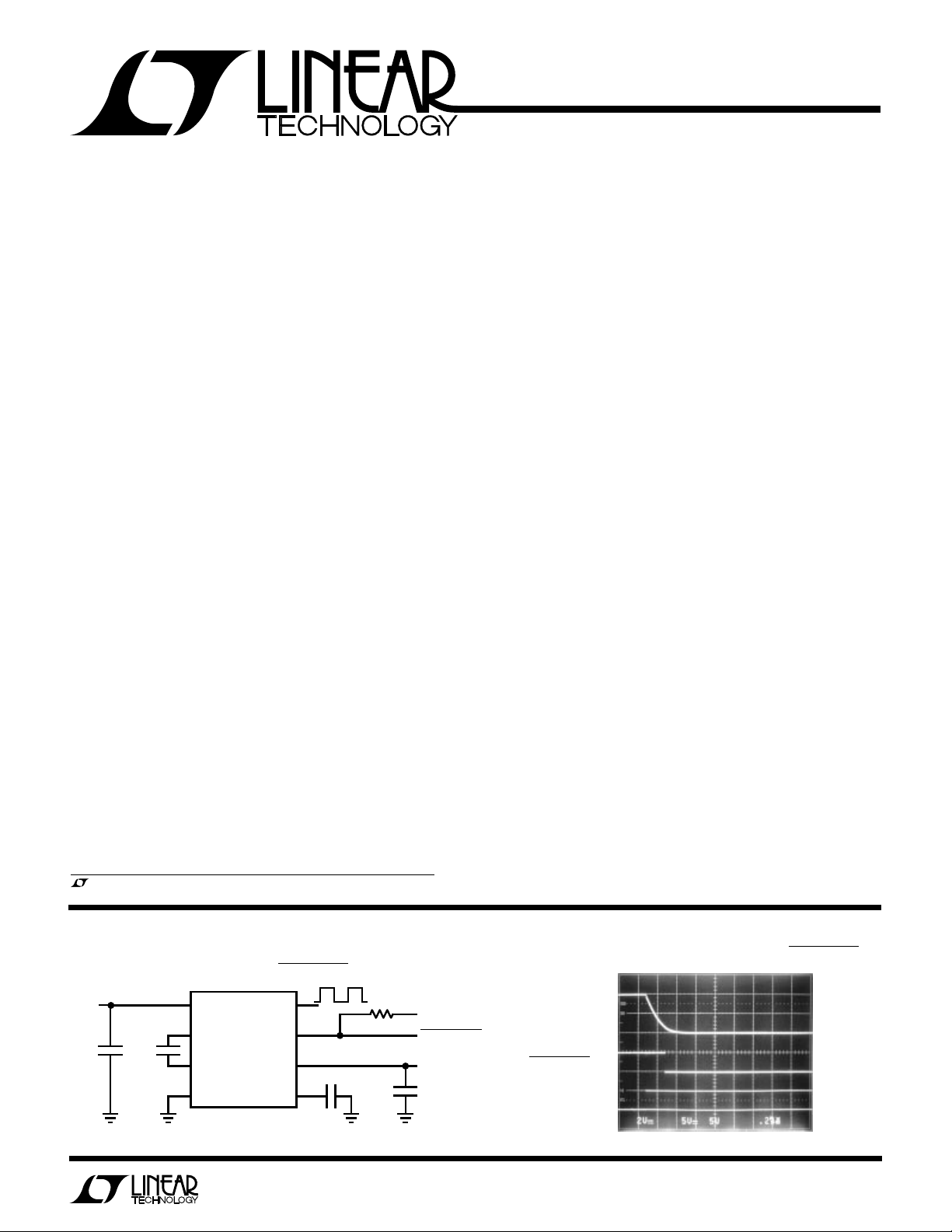
TYPICAL APPLICATION
–4V Generator with Power Valid
5V
0.1µF
C1
*OPTIONAL
0.1µF
1
V
2
C2
C1
3
C1
4
GND
SYNC/SD
CC
+
LTC1429-4CS8
–
REG
OUT
COMP
8
7
6
5
U
*C3
0.001µF
10k
5V
POWER VALID
V
+
= –4V AT 10mA
OUT
C4
3.3µF
LTC1429 • TA01
Waveforms for –4V Generator with Power Valid
0V
V
OUT
–4V
POWER VALID
SYNC/SD
5V
0V
5V
0V
0.2ms/DIV
LTC1429 • TA02
1
Page 2
LTC1429
TOP VIEW
S PACKAGE
14-LEAD PLASTIC SO
1
2
3
4
5
6
7
14
13
12
11
10
9
8
NC
C1
+
C1
–
C2
+
C2
–
GND
R0
V
CC
SYNC/SD
REG
OUT
ADJ
R
ADJ
R1
WW
W
U
ABSOLUTE MAXIMUM RATINGS
(Note 1)
Supply Voltage (Note 2)............................................. 9V
Output Voltage.............................................0.3V to –9V
Total Voltage, VCC to V
(Note 2) ......................... 12V
OUT
Input Voltage (SYNC/SD Pin) ...... –0.3V to (VCC + 0.3V)
Input Voltage (REG Pin).............................–0.3V to 12V
U
W
PACKAGE/ORDER INFORMATION
ORDER PART
NUMBER
LTC1429CS8-4*
S8 PART MARKING
14294
V
1
CC
+
C1
2
–
C1
3
GND
4
8-LEAD PLASTIC SO
TOP VIEW
S8 PACKAGE
8
7
6
5
SYNC/SD
REG
OUT
COMP
Input Voltage (ADJ, RO-1, R
.....................................(V
)
ADJ
– 0.3V) to (V
OUT
Output Short Circuit Duration .......................... Indefinite
Operating Temperature Range ..................... 0°C to 70°C
Storage Temperature Range ................. –65°C to 150°C
Lead Temperature (Soldering, 10 sec).................. 300°C
U
ORDER PART
NUMBER
LTC1429CS
+ 0.3V)
CC
T
= 150°C, θJA = 150°C/W
JMAX
T
= 150°C, θJA = 110°C/W
JMAX
Consult factory for Industrial and Military grade parts. *Contact factory for other output voltages or 8-pin adjustable parts.
ELECTRICAL CHARACTERISTICS
VCC = 3V to 6.5V. C1 = C2 = 0.1µF (Note 4), C
SYMBOL PARAMETER CONDITIONS MIN TYP MAX UNITS
V
REF
I
S
F
SYNC
P
EFF
V
OL
I
REG
I
ADJ
V
IH
V
IL
I
IN
T
ON
2
Reference Voltage ● 1.20 1.24 1.28 V
Supply Current VCC = 3.3V ● 600 1500 µA
Synchronous Clock Frequency (Note 8) VCC ≤ 5V 60 700 2000 kHz
Power Efficiency 65 %
REG Output Low Voltage I
REG Sink Current V
Adjust Pin Current V
SYNC/SD Input High Voltage VCC = 5V ● 2.0 V
SYNC/SD Input Low Voltage VCC = 5V ● 0.8 V
SYNC/SD Input Current V
Turn On Time I
= 3.3µF, F
OUT
= 700kHz with 50% duty cycle square wave, unless otherwise noted.
SYNC
LTC1429CS8/LTC1429CS
= 5V ● 600 1500 µA
V
CC
V
= VCC or GND ● 0.2 5 µA
SYNC/SD
VCC = 6.5V 100 700 2000 kHz
= 1mA ● 0.1 0.8 V
REG
= 0.8V, VCC = 3.3V ● 58 mA
REG
V
= 0.8V, VCC = 5V ● 815 mA
REG
= 1.24V (Note 5) ● 0.01 1 µA
ADJ
= VCC or GND ● ±1 µA
SYNC/SD
= 10mA 200 µs
OUT
Page 3
LTC1429
SUPPLY VOLTAGE (V)
3.0
0
MAXIMUM OUTPUT CURRENT (mA)
5
15
20
25
6.56.0
45
LTC1429 • TPC03
10
3.5 4.0 4.5 5.0 5.5 7.0
30
35
40
V
OUT
= –4V ± 5%
T
A
= 25°C
TRIPLER MODE
DOUBLER MODE
ELECTRICAL CHARACTERISTICS
F
= 700kHz with 50% duty cycle square wave, unless otherwise noted.
SYNC
Tripler Mode,VCC = 3.3V, C1 = C2 = 0.1µF (Note 4), C
= 3.3µF,
OUT
LTC1429CS
SYMBOL PARAMETER CONDITIONS MIN TYP MAX UNITS
∆V
OUT
Output Regulation –1.24V ≥ V
–4V ≥ V
ISCOutput Short Circuit Current V
V
RIP
Output Ripple Voltage I
= 0V ● 35 75 mA
OUT
= 5mA, V
OUT
Doubler Mode, VCC = 5V, C1 = 0.1µ F, C2 = 0 (Note 4), C
OUT
≥ –5V, 0 ≤ I
OUT
OUT
= 3.3µF, F
OUT
≥ –4V, 0 ≤ I
≤ 12mA ● 15 %
OUT
≤ 8mA ● 25 %
OUT
= –4V 5 mV
=700kHz with 50% duty cycle, unless otherwise noted.
SYNC
LTC1429CS8/LTC1429CS
SYMBOL PARAMETER CONDITIONS MIN TYP MAX UNITS
∆V
OUT
V
OUT
I
SC
V
RIP
The ● denotes specifications which apply over the full operating
temperature range.
Note 1: Absolute Maximum Ratings are those values beyond which the life
of the device may be impaired.
Note 2: Setting output to < –7V will exceed the total voltage maximum
rating with a 5V supply. With supplies higher than 4V the output should
never be set to exceed (V
Note 3: All currents into device pins are positive; all currents out of device
pins are negative. All voltages are referenced to ground, unless otherwise
specified. All typicals are given at T
Note 4: C1 = C2 = 0.1µF means the specifications apply to tripler mode
where V
Output Regulation – 1.24V ≥ V
Output Voltage V
Output Short Circuit Current V
Output Ripple Voltage I
– 12V).
CC
= 25°C.
A
– V
CC
= 3.3VCC (LTC1429CS only; the LTC1429CS8 cannot be
OUT
≥ –4V, 0 ≤ I
–4V ≥ V
OUT
OUT
OUT
OUT
≥ –4.5V, 0 ≤ I
OUT
Set to –4V, 0 ≤ I
OUT
= 0V ● 80 125 mA
= 5mA, V
= –4V 10 mV
OUT
≤ 10mA ● 15 %
OUT
≤ 10mA (Note 6) ● 25 %
OUT
≤ 10mA ● –3.80 –4.00 –4.20 V
connected in tripler mode), with C1 connected between C1
C2 connected between C2
– V
V
CC
= 2VCC; for the LTC1429CS, this means C1 connects from C1
OUT
to C2– with C1– and C2+ floating. For the LTC1429CS8 in doubler mode,
C1 connects from C1
+
and C2–. C2 = 0 implies doubler mode where
+
to C1– ; there are no C2 pins.
+
and C1– and
Note 5: Adjustable output parts only; does not apply to fixed output parts.
Note 6: For output voltages below –4.5V, the LTC1429 may reach 50%
duty cycle and fall out of regulation with heavy load or low input voltages.
Beyond this point, the output will follow the input with no regulation.
Note 7: LTC1429 will operate with square wave of 40% to 60% duty cycle.
For best performance, use a square wave with 50% duty cycle.
Note 8: Maximum frequency is not tested. Typical part can be used
beyond 2MHz.
+
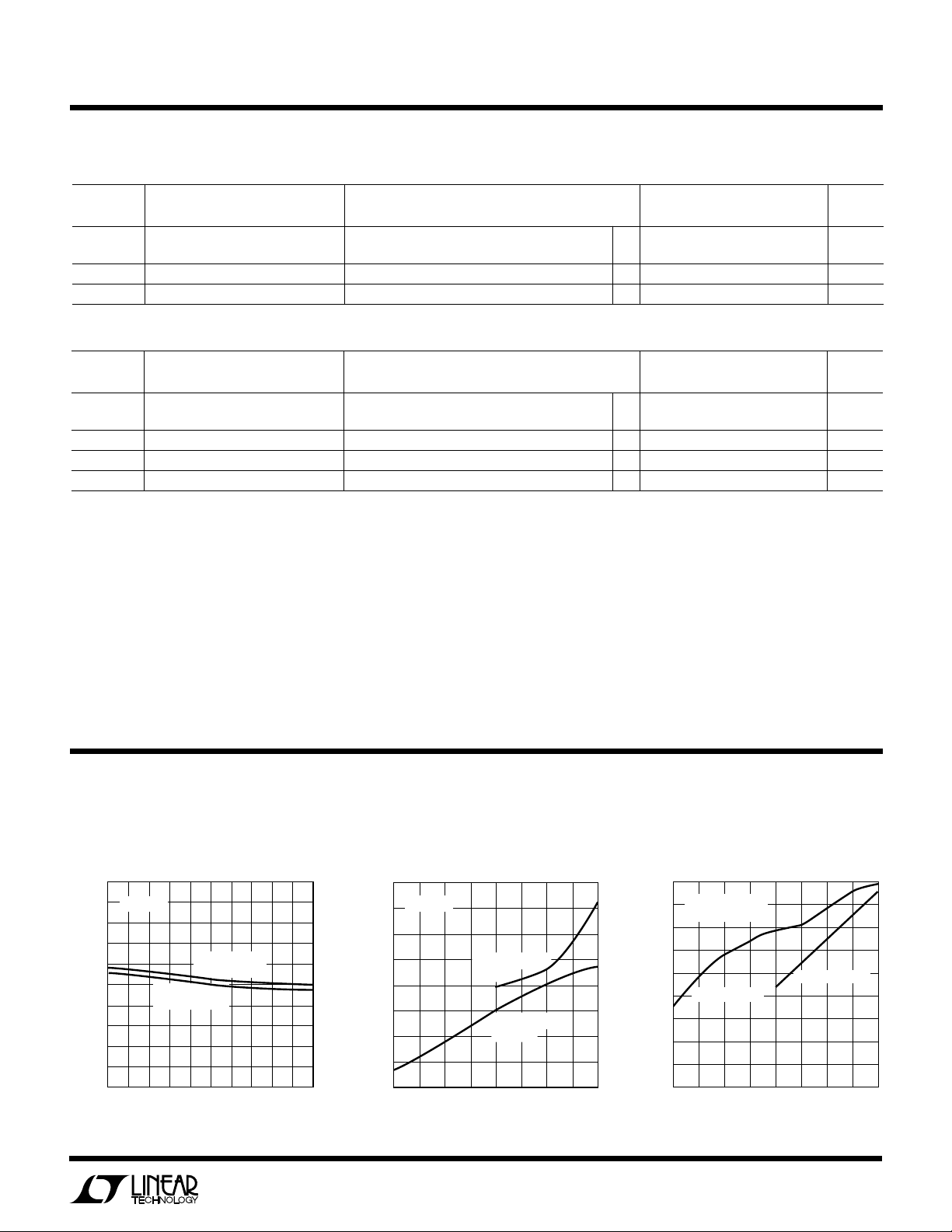
TYPICAL PERFORMANCE CHARACTERISTICS
(See Test Circuits; Figure 1 for Doubler Mode, Figure 2 for Tripler Mode)
Output Voltage vs Output Current Output Voltage vs Supply Voltage
–4.10
–4.08
–4.06
–4.04
–4.00
–3.96
OUTPUT VOLTAGE (V)
– 3.94
–3.92
TA = 25°C
–4.02
–3.98
–3.90
0
VCC = 5V
DOUBLER MODE
213579
VCC = 3.3V
TRIPLER MODE
6
4
OUTPUT CURRENT (mA)
W
8
LTC1429 • TPC01
U
Maximum Output Current vs
Supply Voltage
–4.08
3.0
TA = 25°C
3.5
4.0
SUPPLY VOLTAGE (V)
DOUBLER MODE
= 5mA
I
L
TRIPLER MODE
= 5mA
I
L
5.0
4.5
5.5
6.0
LTC1429 • TPC02
6.5
7.0
–4.07
–4.06
–4.05
–4.04
–4.03
OUTPUT VOLTAGE (V)
–4.02
–4.01
10
–4.00
3
Page 4
LTC1429
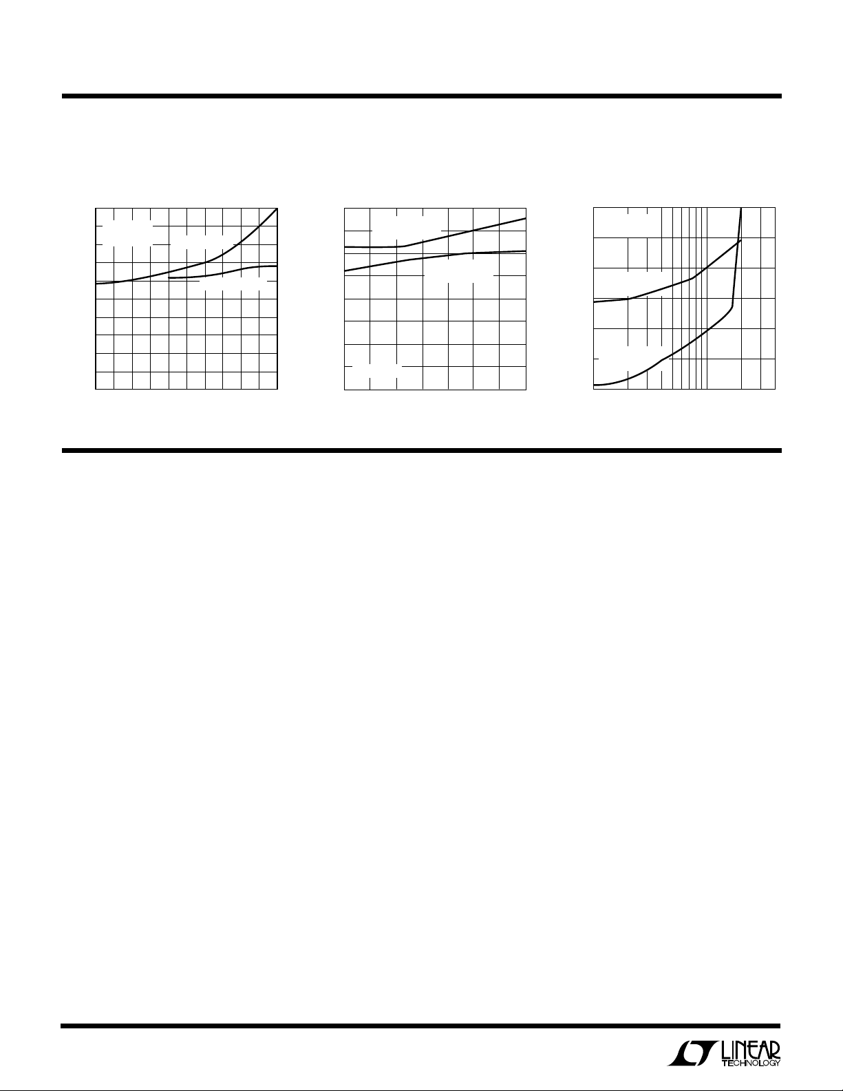
INPUT FREQUENCY (kHz)
100
SUPPLY CURRENT (µA)
750
700
650
600
550
500
450
1000 2000 4000
LTC1429 • TPC06
TA = 25°C
I
LOAD
= 0mA
DOUBLER MODE
V
CC
= 5V
TRIPLER MODE
V
CC
= 3.3V
W
U
TYPICAL PERFORMANCE CHARACTERISTICS
(See Test Circuits: Figure 1 for Doubler Mode, Figure 2 for Tripler Mode)
Supply Current vs Supply Voltage Supply Current vs Temperature
1000
SUPPLY CURRENT (µA)
900
800
700
600
500
400
300
200
100
V
= –4V
OUT
= 25°C
T
A
0
4.03.5 4.5 5.5 6.5 7.5
3.0
TRIPLER MODE
5.0
SUPPLY VOLTAGE (V)
DOUBLER MODE
6.0
7.0
LTC1429 • TPC04
8.0
800
700
600
500
400
300
SUPPLY CURRENT (µA)
200
100
V
CC
DOUBLER MODE
V
= –4V
OUT
0
10 20 40
0
= 5V
VCC= 3.3V
TRIPLER MODE
30
TEMPERATURE (˚C)
50 60 70
LTC1429 • TPC05
UUU
PIN FUNCTIONS
Supply Current vs
Input Frequency
Pin numbers are shown as (LTC1429CS/LTC1429CS8).
NC (Pin 1/NA): No Internal Connection.
+
C1
(Pin 2/Pin 2): C1 Positive Input. Connect an 0.1µF
capacitor between C1+ and C1–. With the LTC1429CS in
doubler mode, connect a 0.1µF capacitor from C1+ to C2–.
–
C1
(Pin 3/Pin 3): C1 Negative Input. Connect a 0.1µF
capacitor from C1+ to C1–. With the LTC1429CS in doubler
mode only, C1– should float.
C2+ (Pin 4/NA): C2 Positive Input. In tripler mode, connect
a 0.1µF capacitor from C2+ to C2– . This pin is used with
the LTC1429CS in tripler mode only; in doubler mode, this
pin should float.
C2– (Pin 5/NA): C2 Negative Input. In tripler mode, connect a 0.1µ F capacitor from C2+ to C2–. In doubler mode,
connect a 0.1µF capacitor from C1+ to C2–.
GND (Pin 6/Pin 4): Ground. Connect to a low-impedance
ground. A ground plane will help to minimize regulation
errors.
R0 (Pin 7/NA): Internal Resistor String-1st Tap. See Table
3 in the Applications Information section for information
on internal resistor string pin connections vs output
voltage.
R1 (Pin 8/NA): Internal Resistor String-2nd Tap.
4
R
(Pin 9/NA): Internal Resistor String Output. Connect
ADJ
this pin to ADJ to use the internal resistor divider. See
Table 3 in the Applications Information section for information on internal resistor string pin connections vs
output voltage.
ADJ (COMP for fixed output versions) (Pin 10/Pin 5):
Output Adjust/Compensation. For adjustable parts, this
pin is used to set the output voltage. The output voltage
should be divided down with a resistor divider and fed
back to this pin to set the regulated output voltage. The
resistor divider can be external or the internal divider
string can be used if it can provide the required output
voltage. Typically the resistor string should draw ≥ 10µ A
from the output to minimize errors due to the bias current
at the adjust pin. Fixed output parts have the internal
resistor string connected to this pin inside the package;
the pin can be used to trim the output voltage if desired. It
can also be used as an optional feedback compensation
pin to reduce output ripple on both adjustable and fixed
output voltage parts. See the Applications Information
section for more on compensation and output ripple.
OUT (Pin 11/Pin 6): Negative Voltage Output. This pin
must be bypassed to ground with a 1.0µF or larger
capacitor; it must be at least 3.3µF to provide specified
output ripple. The size of the output capacitor has a strong
Page 5

PIN FUNCTIONS
LTC1429
UUU
effect on output ripple; see the Applications Information
section for more details.
REG (Pin 12/Pin 7): This is an open drain output that pulls
low when the output voltage is within 5% of the set value.
It will sink 10mA to ground with a 5V supply. The external
circuitry must provide a pull-up or REG will not swing high.
The voltage at REG may exceed VCC; it can be pulled up to
12V above ground without damage.
SYNC/SD (Pin 13/Pin 8): Synchronous Clock Input. A
minimum input clock frequency (60kHz with VCC ≤ 5V and
100kHz with VCC = 6.5V) must be applied to this input to
keep the LTC1429 operating normally. An input clock
below the minimum frequency may cause the charge
TEST CIRCUITS
F
5V
1
V
2
0.1µF10µF
C1
3
C1
4
GND
SYNC/SD
CC
+
LTC1429-4CS8
–
REG
OUT
COMP
8
7
6
5
SYNC
0.001µF
= 700kHz
V
3.3µF
+
= –4V ± 5%
OUT
LTC1429 • TC01
pump to operate erratically or the device to shut down. A
logic high or low at the SYNC/SD pin will put the device
into SHUTDOWN and drop the supply current to 0.2µA.
The LTC1429 will operate with input square wave of 40%
to 60% duty cycle. For best performance, use a square
wave of 50% duty cycle.
VCC (Pin 14/Pin 1): Power Supply. This requires an input
voltage between 3V and 6.5V. Certain combinations of
output voltage and operating mode may place additional
restrictions on the input voltage; see the Applications
Information section for details. VCC must be bypassed to
ground with at least a 0.1µF capacitor, placed in close
proximity to the chip; again, see the Applications Information section.
10µF
+
10
0.001µF
9
8
NC
F
3.3µF
SYNC
= 700kHz
V
= –4V ± 5%
OUT
13
7
NC
11
+
0.1µF
0.1µF
2
3
4
5
VIN = 3.3V
+
C1
–
C1
LTC1429CS
+
C2
–
C2
14
V
CC
SYNC/SD
GND
6
R
ADJ
ADJ
R1
R0
OUT
Figure 1. Doubler Mode
U
WUU
APPLICATIONS INFORMATION
MODES OF OPERATION
The LTC1429 uses a charge pump to generate a negative
output voltage that can be regulated to a value either
higher or lower than the original input voltage. It has two
modes of operation: a doubler inverting mode, which can
provide a negative output equal to or less than the positive
power supply, and a tripler inverting mode, which can
provide negative output voltages either larger or smaller in
magnitude than the original positive supply. The tripler
LTC1429 • TC02
Figure 2. Tripler Mode
offers greater versatility and wider input range but requires four external capacitors and a 14-pin package; the
doubler offers the SO-8 package and requires only three
external capacitors. The optional compensation capacitor
at ADJ/COMP is used to reduce the ripple output voltage.
Doubler Mode
This mode allows the LTC1429 to generate negative
output voltage magnitudes up to that of the supply voltage,
5
Page 6

LTC1429
U
WUU
APPLICATIONS INFORMATION
creating a voltage between VCC and OUT of up to 2 × VCC.
In doubler mode, the LTC1429 uses a single flying capacitor to invert the input supply voltage and the output voltage
is stored on the output bypass capacitor between switch
cycles. The LTC1429CS8 is always configured in doubler
mode and has only one pair of flying capacitor pins (Figure
3a). The LTC1429CS can be configured in doubler mode by
connecting a single flying capacitor between the C1+ and
C2– pins; C1– and C2+ should be left floating (Figure 3b).
(c)
14
13
12
11
10
9
8
LTC1429 • F03
V
1
LTC1429CS8
2
C1
C1+
3
C1
4
SO-8 DOUBLER MODE
(b)
14
13
12
11
10
9
8
1
LTC1429CS
2
+
C1
3
–
C1
8
7
–
(a)
6
5
C1
4
+
C2
5
–
C2
6
7
S0-14 DOUBLER MODE
1
2
C1
C2
C1
3
C1
4
C2
5
C2
6
7
SO-14 TRIPLER MODE
LTC1429CS
+
–
+
–
Figure 3. Flying Capacitor Connections
Tripler Mode
The LTC1429CS can be used in a tripler mode which can
generate negative output voltages up to twice the supply
voltage; the total voltage between the VCC and OUT pins is
3 × VCC. Tripler mode can be used to generate –5V from
a single positive 3.3V supply, for example. Tripler mode
requires two external flying capacitors. The first connects
between C1+ and C1– and the second between C2+ and C2
(Figure 3c). Because of the relatively high voltages that can
be generated in this mode, care must be taken to ensure
that the total input-to-output voltage never exceeds 12V,
or the LTC1429 may be damaged. This is possible with
supply voltages above 4V in tripler mode and above 6V in
doubler mode, although in most applications the output
voltage will be kept in check by the regulation loop. As the
input supply voltage rises, the allowable output voltage
drops, finally reaching –4V with a 8.5V supply. To avoid
this problem, use doubler mode whenever possible with
high input supply voltages.
THEORY OF OPERATION
A block diagram of the LTC1429 is shown in Figure 4. The
heart of the LTC1429 is the charge pump core, shown in the
dashed line. It generates a negative output voltage by first
charging the flying caps between VCC and ground. It then
CC
–
DELAY
SYNC/SD
S
R
SHUTDOWN
+
C
S1 S5
+
C1
Q
S2
C1
S4 S6
–
C1
S3
+
C2
C2
–
C2
S7
+
COMP 1
–
124k
226k
100k
50k
ADJ/COMP
V
R
REG
OUT
ADJ
R1*
R0*
*
OUT
INTERNALLY
CONNECTED FOR
FIXED OUTPUT
VOLTAGE PARTS
+
COMP 2
*LTC1429CS14 ONLY
LTC1429 • F04
1.24V
60mV
1.18V
–
V
OUT
Figure 4. Block Diagram
6
Page 7

LTC1429
U
WUU
APPLICATIONS INFORMATION
stacks the flying caps on top of each other and connects the
top of the stack to ground; this forces the bottom of the
stack to a negative voltage. The charge on the flying
capacitors is transferred to the output bypass cap, leaving
it charged to the negative output voltage. This process is
driven by the external 700kHz clock via the SYNC/SD pin.
Figure 4 shows the charge pump configured in tripler
mode. With the external input clock low, C1 and C2 are
charged to VCC by S1, S3, S5 and S7. At the next rising
clock edge, S1, S3, S5 and S7 open and S2, S4 and S6
close, stacking C1 and C2 on top of each other. S2
connects C1+ to ground, S4 connects C1– to C2+ and C2
is connected to the output by S6. The charge in C1 and C2
is transferred to C
Doubler mode works the same way except that the single
flying capacitor (C1) is connected between C1+ and C2–.
S3, S4 and S5 don’t do anything useful in doubler mode.
C1 is charged initially by S1 and S7, and connected to the
output by S2 and S6.
The output voltage is monitored by COMP1, which compares a divided replica of the output at ADJ (COMP for fixed
output parts) to the internal reference. At the beginning of
a cycle, the clock is low, forcing the output of the AND gate
low and charging the flying caps. The next rising clock
edge sets the RS latch, setting the charge pump to transfer
charge from the flying caps to the output capacitor. As
long as the output is below the set point, COMP1 stays low,
the latch stays set and the charge pump runs at the duty
cycle of the input clock signal, gated through the AND gate.
As the output approaches the set voltage, COMP1 will trip
whenever the divided signal exceeds the internal 1.24V
reference, relative to OUT. This resets the RS latch and
truncates the clock pulses, internally reducing the amount
of charge transferred to the output capacitor and regulating the output voltage. If the output exceeds the set point,
COMP1 stays high, inhibiting the RS latch and disabling
the charge pump.
COMP2 also monitors the divided signal at ADJ, but it is
connected to a 1.18V reference, 5% below the main reference
voltage. When the divided output exceeds this lower reference voltage, indicating that the output is within 5% of the set
value, COMP2 goes high, turning on the REG output transistor. This is an open drain N-channel device capable of sinking
, setting it to a negative voltage.
OUT
–
8mA with a 3.3V VCC and 15mA with a 5V VCC. When in “off”
state (divided output more than 5% below V
be pulled above VCC without damage, up to a maximum of
12V above ground. Note that the REG output only indicates
if the magnitude of the output is
set point by 5% (i.e., V
the magnitude of the output is forced
tude of the set point (i.e., to –6V when the output is set for
–5V) the REG output will stay low.
OUTPUT RIPPLE
Output ripple in the LTC1429 comes from two sources:
voltage droop at the output capacitor between clocks and
frequency response of the regulation loop. Voltage droop
is easy to calculate. With a typical external input clock
frequency of 700kHz, the charge on the output capacitor
is refreshed once every 1.43µs. With a 15mA load and a
3.3µF output capacitor, the output will droop by:
I
LOAD
There can be a significant ripple component when the
output is heavily loaded, especially if the output capacitor
is small or the external input clock frequency is low. If
absolute minimum output ripple is required, a 10µF or
greater output capacitor, high input clock rate (F
lower value (<0.1µF) of flying capacitor should be used.
Regulation loop frequency response is the other major
contributor to output ripple. The LTC1429 regulates the
output voltage by limiting the amount of charge transferred to the output capacitor on a cycle-by-cycle basis.
The output voltage is sensed at the ADJ pin (COMP for
fixed output versions) through an internal or external
resistor divider from the OUT pin to ground. As the flying
caps are first connected to the output, the output voltage
begins to change quite rapidly. As soon as it exceeds the
set point, COMP1 trips, switching the state of the charge
pump and stopping the charge transfer. Because the RC
time constant of the capacitors and the switches is quite
short, the ADJ pin must have a wide AC bandwidth to be
able to respond to the output in time. External parasitic
capacitance at the ADJ pin can reduce the bandwidth to the
point where the comparator cannot respond by the time
∆t
× = 15mA ×
)
C
OUT
OUT
)
below
the magnitude of the
> –4.75V for a – 5V set point). If
higher
1.43µs
)
3.3µF
) the drain can
REF
than the magni-
= 6.5mV
)
SYNC
) and
7
Page 8

LTC1429
LTC1429CS8-4
V
CC
5V
C1
+
C1
–
4
1
6
8
5
2
3
OUT
SYNC/SD
0.1µF
1000pF
3.3µF
10Ω
COMP
LTC1429 • F06
GND
+
3.3µF
V
OUT
= –4V
+
0.1µF
F
SYNC
= 700kHz
U
WUU
APPLICATIONS INFORMATION
the clock pulse finishes. When this happens, the comparator will allow a few complete pulses through, then overcorrect and disable the charge pump until the output
drops below the set point. Under these conditions, the
output will remain in regulation, but the output ripple will
increase as the comparator “hunts” for the correct value.
To help prevent this from happening, an external capacitor
can be connected from ADJ (or COMP for fixed output
parts) to ground to compensate for external parasitics and
increase the regulation loop bandwidth (Figure 5). This
sounds counter-intuitive until we remember that the internal reference is generated with respect to OUT, not ground.
The feedback loop actually sees ground as its “output”;
thus the compensation capacitor should be connected
across the “top” of the resistor divider from ADJ (or
COMP) to ground. By the same token, avoid adding
capacitance between ADJ (or COMP) and V
slow down the feedback loop and increase output ripple.
A 1000pF capacitor from ADJ or COMP to ground will
compensate the loop properly under most conditions.
TO CHARGE
PUMP
; this will
OUT
current. The clock signal should have a duty cycle between
40% and 60% for proper regulation loop performance.
The LTC 1429 can be shut down by stopping the clock. An
internal circuit monitors the time between clock edges at
the SYNC/SD pin. If a 10µ s period elapses without a rising
or falling edge, LTC1429 assumes the clock has stopped
and goes into shutdown mode and the quiescent current
drops to below 1µ A. The next clock edge at the SYNC/SD
pin will reawaken the LTC1429. At clock frequencies
below 50kHz (50% duty cycle) the LTC1429 may enter
shutdown mode briefly during each clock cycle causing
erratic operation. Minimum operating frequency should
be kept above 60kHz (above 100kHz with VCC > 5) to
prevent this from happening.
Radiation from the clock signal at the SYNC/SD pin can
interfere with the feedback node at the ADJ/COMP pin
causing errors in the output voltage. The clock line should
be routed away from the circuitry at the ADJ/COMP pin
and should be shielded with a ground plane or with coaxial
cable. A compensation capacitor from the ADJ/COMP pin
to ground can also help to reduce this effect: 0.001µF is
adequate for most applications.
COMP 1
C
ADJ/COMP
V
OUT
C
1000pF
LTC1429 • F05
R1
REF
Figure 5. Regulator Loop Compensation
+
–
1.24V
R2
RESISTORS ARE INTERNAL
FOR FIXED OUTPUT PARTS
EXTERNAL CLOCK
The LTC1429 requires an external clock to operate. This
clock signal should be TTL or CMOS compatible and
should be applied to the SYNC/SD pin. The external clock
allows the user to control the frequency at which the
LTC1429 operates, preventing it from interfering with
other frequency-sensitive circuitry. The LTC1429 can be
synchronized to any frequency between 60kHz (100kHz
for VCC > 5) and 2MHz. Higher clock frequencies can help
reduce output ripple at the cost of additional quiescent
8
OUTPUT FILTERING
If extremely low output ripple (<10mV) is required, additional output filtering is required. Because the LTC1429
uses a high, external control switching frequency, fairly
low value RC or LC networks can be used at the output to
effectively filter the output ripple. With F
= 700kHz, a
SYNC
10Ω series output resistor and a 3.3µ F capacitor will cut
output ripple to below 3mV (see Figure 6). Further reduc-
Figure 6. Output Filter Cuts Ripple Below 3mV
Page 9

LTC1429
U
WUU
APPLICATIONS INFORMATION
tions can be obtained with larger filter capacitors or by
using an LC output filter or higher F
lower value (<0.1µF) of flying capacitor. Also see the
section on Output Capacitor ESR. For applications requiring ripple below 1mV, see the LTC1550/LTC1551 data
sheet.
CAPACITOR SELECTION
Capacitor Sizing
The performance is dependent on the type of capacitors
used. The LTC1429 requires bypass caps to ground for
both the VCC and OUT pins. The input cap provides most
of the LTC1429’s supply current while it is charging the
flying caps. It should be mounted as close to the package
as possible, its value should be equal to or larger than the
flying cap in doubling mode and at least twice the value of
the flying caps in tripling mode. Ceramic capacitors
generally provide adequate performance; avoid using a
tantalum capacitor as the input bypass unless there is at
least a 0.1µF ceramic cap in parallel with it. The charge
pump caps are somewhat less critical, since their peak
currents are limited by the switches inside the LTC1429.
Most applications should use 0.1µF as the flying cap
value; conveniently, ceramic caps are the most common
type of 0.1µF cap and they work well here. Usually the
easiest solution is to use the same type of capacitor for
both the input bypass and flying caps.
clock rate with a
SYNC
each clock cycle. The smaller capacitors draw smaller
pulses of current out of VCC as well, limiting peak currents
and reducing the demands on the input supply. Tables 1
and 2 show recommended values of flying capacitors vs
maximum load capacity at F
= 400kHz and 700kHz
SYNC
respectively.
Table 1. Typical Max Load (mA) vs Flying Capacitor Value at
TA = 25°C, V
FLYING CAPACITOR VCC = 5V VCC = 3.3V
VALUE (µ F) DOUBLER MODE TRIPLER MODE
0.1 22 20
0.047 16 15
0.033 8 11
0.022 4 5
0.01 1 3
Table 2. Typical Max Load (mA) vs Flying Capacitor Value at
TA = 25°C, V
FLYING CAPACITOR VCC = 5V VCC = 3.3V
VALUE (µ F) DOUBLER MODE TRIPLER MODE
0.1 18 25
0.047 17 22
0.033 14 20
0.022 12 17
0.01 3 9
= –4V, F
OUT
= –4V, F
OUT
= 400kHz
SYNC
MAX LOAD (mA) MAX LOAD (mA)
= 700kHz
SYNC
MAX LOAD (mA) MAX LOAD (mA)
Output Capacitor ESR
The output cap performs two functions; it provides output
current to the load during half of the charge pump cycle
and its value helps to set the output ripple voltage. For
applications that are insensitive to output ripple, the
output bypass cap can be as small as 1µF. To achieve
specified low output ripple, a 3.3µF or greater output
capacitor, high input clock rate (F
) and lower value
SYNC
(< 0.1µ F) of flying capacitor should be used. Larger output
caps will reduce output ripple further, at the expense of
turn on time.
In an application where the maximum load current is welldefined and output ripple is critical or input peak currents
need to be minimized, the flying capacitor values can be
tailored to the application. Reducing the value of the flying
capacitors reduces the amount of charge transferred with
Output capacitor the Equivalent Series Resistance (ESR)
is another factor to consider. Excessive ESR in the output
capacitor can fool the regulation loop into keeping the
output artificially low by prematurely terminating the charging cycle. As the charge pump switches to recharge the
output, a brief surge of current flows from the flying caps
to the output cap. This current surge can be as high as
100mA under full load conditions. A typical 3.3µF tantalum
capacitor has 1Ω or 2Ω of ESR; 100mA × 2Ω = 200mV. If
the output is within 200mV of the set point, this additional
200mV surge will trip the feedback comparator and terminate the charging cycle. The pulse dissipates quickly and
the comparator returns to the correct state, but the RS
latch will not allow the charge pump to respond until the
next clock edge. This prevents the charge pump from
9
Page 10

LTC1429
U
WUU
APPLICATIONS INFORMATION
going into very high frequency oscillation under such conditions. It also creates an output error as the feedback loop
regulates based on the top of the spike, not the average value
of the output (Figure 7). The resulting output voltage behaves
as if a resistor of value C
with the output. To minimize this effect, output capacitor ESR
should be as low as possible or smaller value high frequency
bypass (typically a 0.1µ F ceramic) should be added in parallel
with the output capacitor.
CLOCK
LOW ESR
OUTPUT CAP
HIGH ESR
OUTPUT CAP
Figure 7. Output Ripple with Low and High ESR Caps
Note that ESR in the flying caps will not cause the same
condition; in fact, it may actually improve the situation by
cutting the peak currents and lowering the amplitude of
the spike. More flying cap ESR is not necessarily better,
however; as soon as the RC time constant approaches half
of a clock period (the time the capacitors have to share
charge at full duty cycle) the output current capability of
the LTC1429 will begin to diminish. For 0.1µF flying
capacitors and typical 700kHz external clock, this gives a
maximum total series resistance of:
t
1
2
1
= / 0.1µF = 7.14Ω
)
)
2
700kHz
)
C
CLK
FLY
Most of this resistance is already provided by the internal
switches in the LTC1429 (especially in tripler mode). More
than 1Ω or 2Ω of ESR on the flying caps will start to affect
the regulation at maximum load.
× (IPK/I
ESR
V
OUT
V
OUT
)Ω was placed in series
AVE
V
SET
V
OUT
AVERAGE
COMP1
OUTPUT
V
SET
V
OUT
AVERAGE
COMP1
OUTPUT
LTC1429 • F07
1
)
difficult. A resistor divider should be used to divide the
signal at the output to give 1.24V at the ADJ pin
respect to V
reference with respect to V
(Figure 8). The LTC1429 uses a positive
OUT
, not a negative reference
OUT
with
with respect to ground (Figure 4 shows reference connection). Be sure to keep this in mind when connecting the
resistors! If the initial output is not what you expected, try
swapping the two resistors.
6 (4)*
GND
LTC1429
Figure 8. External Resistor Connections
ADJ
OUT
10 (5)*
11 (6)*
LTC1429CS
*(LTC1429CS8)
R1
R2
V
OUT
= –1.24V
(R1 + R2)
R2
LTC1429 • F07
The 14-pin adjustable parts include a built-in resistor
string which can provide an assortment of output voltages
by using different pin-strapping options at the RO, R1 and
R
pins (Table 3). The internal resistors are roughly
ADJ
124k, 226k, 100k and 50k (see Figure 4) giving output
options of –3.5V, – 4V, –4.5V and – 5V. The resistors are
carefully matched to provide accurate divider ratios, but
the absolute values can vary substantially from part to
part. It’s not a good idea to create a divider using an
external resistor and one of the internal resistors unless
the output voltage accuracy is not critical.
Table 3. Output Voltages Using the Internal Resistor Divider
PIN CONNECTIONS OUTPUT VOLTAGE
ADJ - R
ADJ
ADJ - R
ADJ - R
ADJ - R
ADJ - R1 –1.77V
ADJ - R0 –1.38V
ADJ - GND –1.24V
, RO - GND –4.5V
ADJ
, R1 - RO –4.0V
ADJ
, R1-GND – 3.5V
ADJ
–5.0V
RESISTOR SELECTION
Resistor selection is easy with the fixed output versions of
the LTC1429; no resistors are needed! Selecting the right
resistors for the adjustable parts is only a little more
10
There are some oddball output voltages available as well.
They are obtained by connecting ADJ to R0 or R1 and
shorting out some of the internal resistors. If one of them
gives you the output voltage you want, by all means use it!
Page 11

LTC1429
2
3
4
5
10
9
13
8
7
11
ADJ
R
ADJ
SYNC/SD
R1
R0
OUT
C1
+
C1
–
C2
+
C2
–
0.1µF
LTC1429 • TA06
NC
NC
6
14
0.1µF
0.001µF
0.22µF
LTC1429CS
3V ≤ V
CC
≤ 7V
V
CC
GND
3.3µF
V
OUT
= –5V ±5%
AT 10mA
+
1
2
3
4
8
7
6
5
SYNC/SD
REG
OUT
COMP
VCC
C1
+
C2
–
GND
0.001µF
LTC11429 • TA04
3.3µF
–4V BIAS
10k
P-CHANNEL
POWER SWITCH
0.1µF
SYNC/SD
5V
V
BAT
+
LTC1429CS8-4
GaAs
TRANSMITTER
0.1µF
U
WUU
APPLICATIONS INFORMATION
The internal resistor values are the same for the fixed
output versions of the LTC1429 as they are for the adjustable parts. The output voltage can be trimmed, if desired,
by connecting external resistance from the COMP pin to
OUT or ground to alter the divider ratio. As in the adjustable
parts, the absolute value of the internal resistors may vary
significantly from unit to unit. As a result, the further the
trim shifts the output voltage, the less accurate the output
voltage will be. If a precise output voltage other than one
U
TYPICAL APPLICATIONS
3.3V In, –4.5V Out GaAs FET Bias Generator
P-CHANNEL
V
3.3V
BAT
0.22µF
POWER SWITCH
of the available fixed voltages is required, it’s better to use
an adjustable LTC1429 and use precision external resistors. The internal reference is trimmed at the factory to
within 3.5% of 1.24V. With 1% external resistors, the
output will be within 5.5% of the nominal value, even
under worst case conditions.
The LTC1429 can be internally configured with nonstandard fixed output voltages. For details, contact the Linear
Technology Marketing Department.
5V In, –4V Out GaAs FET Bias Generator
SYNC/SD
0.1µF
0.1µF
NC
Minimum Parts Count –4V Generator
5V
2
C1+
3
C1
4
C2
5
C2
8
R1
0.1µF
0.1µF
14
V
CC
SYNC/SD
–
REG
LTC1429CS
+
OUT
–
ADJ
R
R0 GND
76
1
2
3
4
13
12
11
10
9
ADJ
SYNC/SD
VCC
+
C1
LTC1429CS8-4
–
C1
GND
10k
–4.5V BIAS
+
0.001µF
3.3µF
GaAs
TRANSMITTER
LTC1429 • TA03
–5V Supply Generator
8
7
REG
6
OUT
5
COMP
Information furnished by Linear Technology Corporation is believed to be accurate and reliable.
However, no responsibility is assumed for its use. Linear Technology Corporation makes no representation that the interconnection of its circuits as described herein will not infringe on existing patent rights.
+
V
OUT
3.3µF
LTC11429 • TA07
= –4V
11
Page 12

LTC1429
TYPICAL APPLICATIONS
1mV Ripple, 5V In, –4V Out GaAs FET Bias Generator
U
V
P-CHANNEL
POWER SWITCH
BAT
SYND/SD
5V
0.1µF
0.1µF
PACKAGE DESCRIPTION
0.010 – 0.020
(0.254 – 0.508)
0.008 – 0.010
(0.203 – 0.254)
*THESE DIMENSIONS DO NOT INCLUDE MOLD FLASH OR PROTRUSIONS.
MOLD FLASH OR PROTRUSIONS SHALL NOT EXCEED 0.006 INCH (0.15mm).
× 45°
0.016 – 0.050
0.406 – 1.270
(1.346 – 1.752)
0°– 8° TYP
0.053 – 0.069
1
VCC
2
+
C1
LTC1429CS8-4
3
–
C2
4
GND
SYNC/SD
REG
OUT
COMP
0.001µF
8
7
6
5
10kΩ
100µH
10µF
+
+
–4V BIAS
10µF
GaAs
TRANSMITTER
LTC1429 • TA05
U
Dimension in inches (millimeters) unless otherwise noted.
0.189 – 0.197*
(4.801 – 5.004)
8
1
7
2
0.014 – 0.019
(0.355 – 0.483)
S8 Package
8-Lead Plastic SOIC
0.004 – 0.010
(0.101 – 0.254)
0.050
(1.270)
BSC
SO8 0294
0.228 – 0.244
(5.791 – 6.197)
5
6
0.150 – 0.157*
(3.810 – 3.988)
3
4
13
2
0.337 – 0.344*
(8.560 – 8.738)
12
11 10
3
4
8
9
0.150 – 0.157*
(3.810 – 3.988)
5
7
6
0.010 – 0.020
(0.254 – 0.508)
0.008 – 0.010
(0.203 – 0.254)
*THESE DIMENSIONS DO NOT INCLUDE MOLD FLASH OR PROTRUSIONS.
MOLD FLASH OR PROTRUSIONS SHALL NOT EXCEED 0.006 INCH (0.15mm).
× 45°
0.016 – 0.050
0.406 – 1.270
0° – 8° TYP
0.053 – 0.069
(1.346 – 1.752)
0.014 – 0.019
(0.355 – 0.483)
S Package
14-Lead Plastic SOIC
0.004 – 0.010
(0.101 – 0.254)
0.050
(1.270)
TYP
0.228 – 0.244
(5.791 – 6.197)
14
1
RELATED PARTS
PART NUMBER DESCRIPTION COMMENTS
LT1121 Micropower Low Dropout Regulators with Shutdown 0.4V Dropout Voltage at 150mA, Low Noise, Switched
Capacitor Regulated Voltage Inverter
LTC1261 Switched Capacitor Regulated Voltage Inverter Selectable Fixed Output Voltage
LTC1550/LTC1551 Low Noise Switched Capacitor Regulated Voltage Inverter GaAs FET Bias with Linear Regulator 1mV Ripple
LT/GP 0695 10K • PRINTED IN USA
LINEAR TECHNOLOGY CORPORATION 1995
12
Linear Technology Corporation
1630 McCarthy Blvd., Milpitas, CA 95035-7487
(408) 432-1900
●
FAX
: (408) 434-0507
●
TELEX
: 499-3977
SO14 0294
 Loading...