

Page 1
FEATURES
■
Allows Safe Board Insertion and Removal
from a Live Backplane
■
System Reset Output with Programmable Delay
■
Programmable Electronic Circuit Breaker
■
User-Programmable Supply Voltage Power-Up Rate
■
High Side Driver for an External N-Channel FET
■
Controls Supply Voltages from 2.7V to 12V
■
Undervoltage Lockout
■
Soft Reset Input
■
Glitch Filter on RESET
U
APPLICATIO S
LTC1422
Hot Swap Controller
U
DESCRIPTIO
TM
The LTC®1422 is an 8-pin Hot Swap
allows a board to be safely inserted and removed from a
live backplane. Using an external N-channel pass transistor, the board supply voltage can be ramped up at a
programmable rate. A high side switch driver controls the
N-channel gate for supply voltages ranging from 2.7V to
12V.
A programmable electronic circuit breaker protects
against shorts. The RESET output can be used to generate
a system reset when the supply voltage falls below a
programmable voltage. The ON pin can be used to cycle
the board power or to generate a soft reset.
controller that
■
Hot Board Insertion
■
Electronic Circuit Breaker
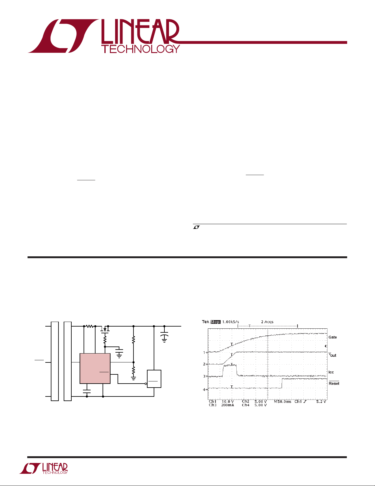
TYPICAL APPLICATIO
5V Hot Swap
Q1
R1
MTB50N06V
VCCSENSE GATE
ON
CONNECTOR 1
0.005Ω
R2
10Ω
5%
8
76
FB
LTC1422
RESET
GNDTIMER
34
C2
0.33µF
52
1
V
ON/RESET
GND
CC
CONNECTOR 2
PLUG-IN CARDBACKPLANE
U
C1
0.1µF
R3
6.81k
1%
R4
2.43k
1%
µP
RESET
The LTC1422 is available in 8-pin PDIP and SO packages.
, LTC and LT are registered trademarks of Linear Technology Corporation.
Hot Swap is a trademark of Linear Technology Corporation.
V
OUT
+
5V
C
LOAD
1422 TA01
1
Page 2
LTC1422
1
2
3
4
8
7
6
5
TOP VIEW
N8 PACKAGE
8-LEAD PDIP
S8 PACKAGE
8-LEAD PLASTIC SO
RESET
ON
TIMER
GND
V
CC
SENSE
GATE
FB
WW
W
U
ABSOLUTE MAXIMUM RATINGS
PACKAGE
/
O
RDER I FOR ATIO
WU
(Note 1)
Supply Voltage (VCC) ........................................... 13.2V
Input Voltage (TIMER, SENSE) ... – 0.3V to (VCC + 0.3V)
Input Voltage (FB, ON)........................... –0.3V to 13.2V
Output Voltage (RESET) ........................ –0.3V to 13.2V
Output Voltage (GATE) ............................. –0.3V to 20V
Operating Temperature Range
ORDER PART
NUMBER
LTC1422CN8
LTC1422CS8
LTC1422IN8
LTC1422IS8
LTC1422C ............................................... 0°C to 70°C
T
LTC1422I........................................... –40°C to 85°C
Storage Temperature Range ................ –65°C to 150°C
Lead Temperature (Soldering, 10 sec)................. 300°C
Consult factory for Military grade parts.
ELECTRICAL CHARACTERISTICS
temperature range, otherwise specifications are at T
SYMBOL PARAMETER CONDITIONS MIN TYP MAX UNITS
DC Characteristics
I
CC
V
LKO
V
LKH
V
FB
∆V
V
FBHST
V
TM
∆V
V
TMHST
I
TM
V
CB
I
CP
∆V
V
ONHI
V
ONLO
V
ONHYST
V
OL
I
PU
t
RST
Note 1: Absolute Maximum Ratings are those values beyond which the life
of a device may be impaired.
VCC Supply Current ON = V
VCC Undervoltage Lockout ● 2.40 2.47 2.55 V
VCC Undervoltage Lockout Hysteresis 120 mV
FB Pin Voltage Threshold ● 1.220 1.232 1.244 V
FB Pin Threshold Line Regulation 3V ≤ V
FB
FB Pin Voltage Threshold Hysteresis 2.0 mV
TIMER Pin Voltage Threshold ● 1.208 1.232 1.256 V
TIMER Pin Threshold Line Regulation 3V ≤ VCC ≤ 12V ● 215 mV
TM
TIMER Pin Voltage Threshold Hystersis 45 mV
TIMER Pin Current Timer On, GND ≤ V
Timer Off, V
Circuit Breaker Trip Voltage VCB = (VCC – V
GATE Pin Output Current Charge Pump On, V
Charge Pump Off, V
External N-Channel Gate Drive V
GATE
ON Pin Threshold High ● 1.25 1.30 1.35 V
ON Pin Threshold Low ● 1.20 1.23 1.26 V
ON Pin Hysteresis 80 mV
Output Low Voltage RESET, IO = 3mA ● 0.14 0.4 V
Logic Output Pull-Up Current RESET = GND –12 µA
Soft Reset Time ● 22 30 38 µs
GATE
The ● denotes the specifications which apply over the full operating
= 25°C. V
A
CC
≤ 12V ● 0.5 2.5 mV
CC
– V
CC
= 5V unless otherwise noted.
CC
≤ 1.5V ● –2.5 –2.0 –1.5 µA
TIMER
= 1.5V 10 mA
TIMER
) ● 44 50 64 mV
SENSE
= GND ● –12 –10 –8 µA
GATE
= V
GATE
= 150°C, θJA = 130°C/W (N)
JMAX
= 150°C, θJA = 150°C/W (S)
T
JMAX
CC
S8 PART MARKING
1422
1422I
● 0.65 1.00 mA
10 mA
● 10 12 14 V
2
U
Page 3
UW
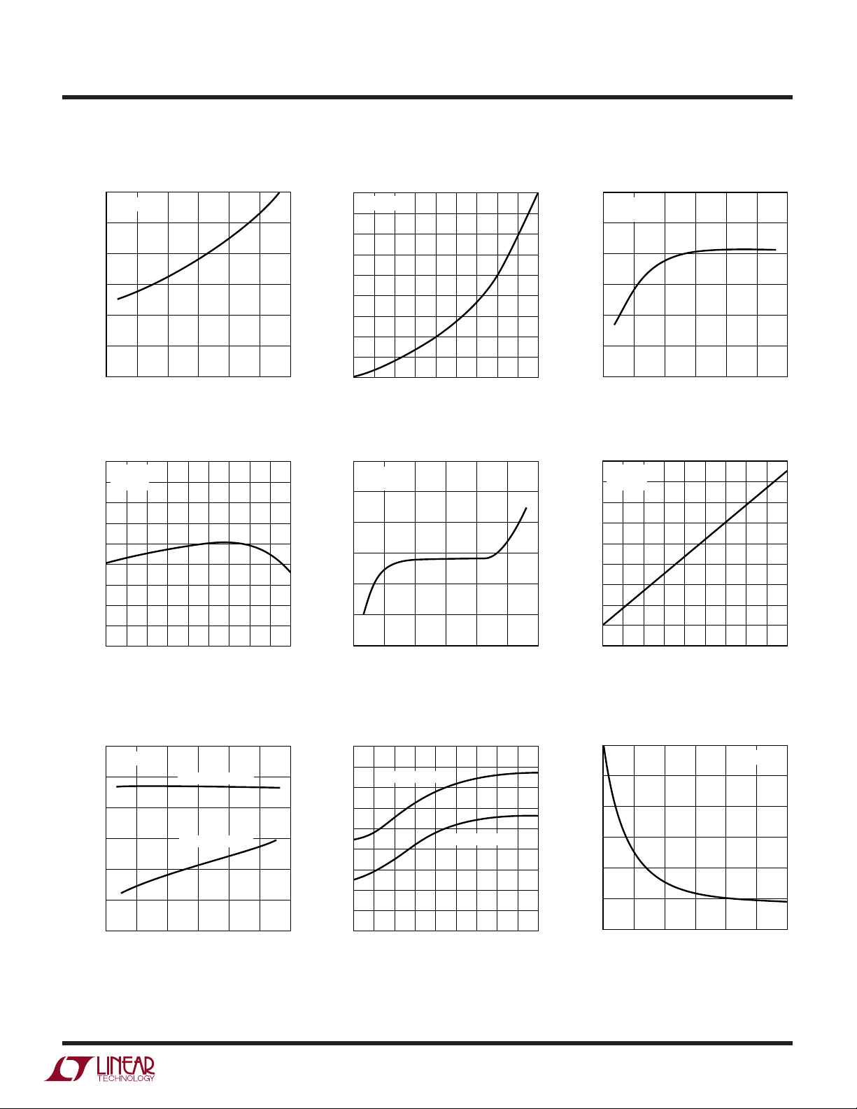
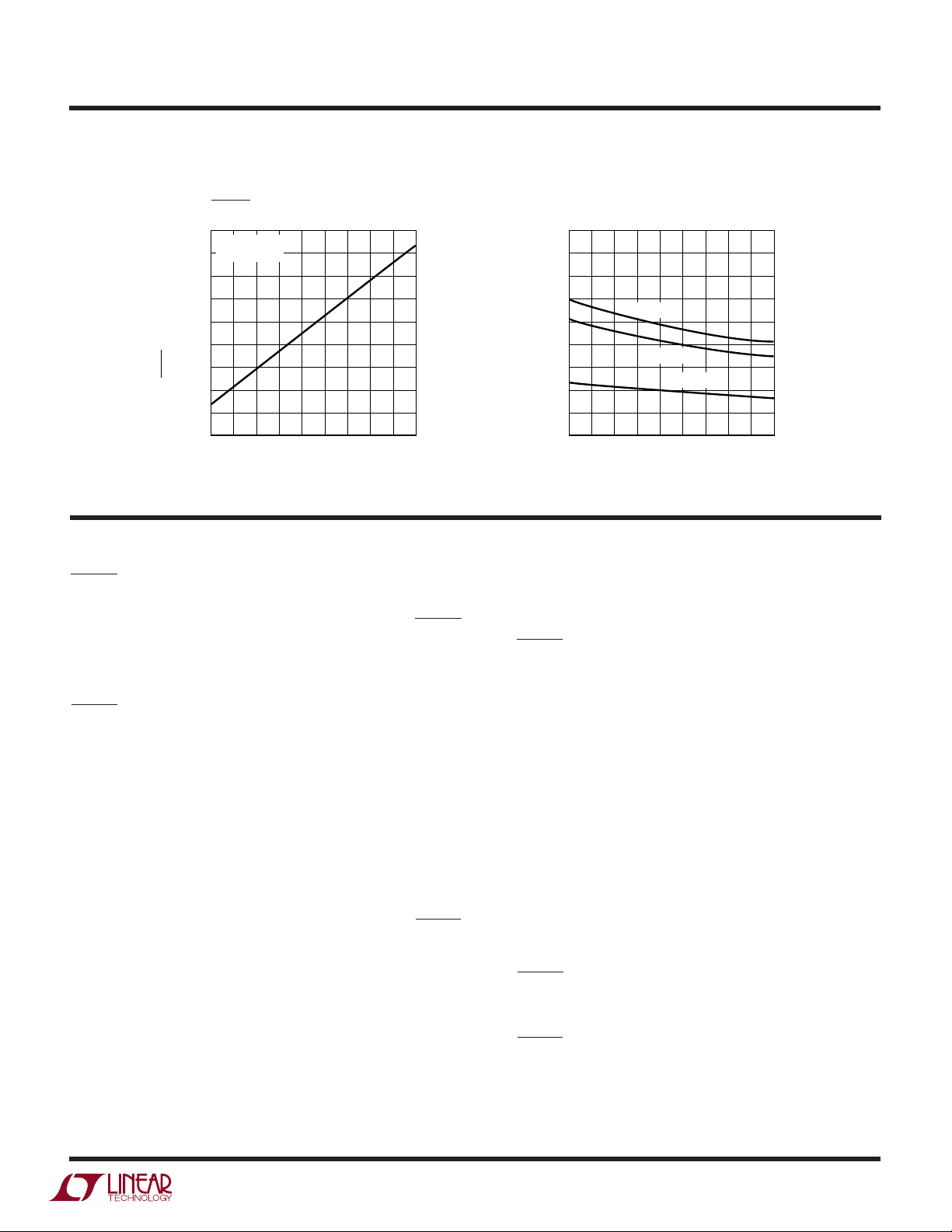
TYPICAL PERFORMANCE CHARACTERISTICS
LTC1422
Supply Current vs Supply Voltage Supply Current vs Temperature
1200
TA = 25°C
1000
800
600
400
SUPPLY CURRENT (µA)
200
0
2
6810
4
SUPPLY VOLTAGE (V)
Gate Voltage vs Temperature
18.2
VCC = 5V
= 0A
I
18.0
G
17.8
17.6
17.4
17.2
17.0
GATE VOLTAGE (V)
16.8
16.6
16.4
–55
–35
5
–15
25
TEMPERATURE (°C)
45
12 14
1422 G01
125
85
105
65
1422 G04
775
VCC = 5V
750
725
700
675
650
625
SUPPLY CURRENT (µA)
600
575
550
–55
–35
5
–15
25
TEMPERATURE (°C)
45
Gate Current vs Supply Voltage
16
TA = 25°C
= 0V
V
G
14
12
10
8
GATE CURRENT (µA)
6
4
2
6810
4
SUPPLY VOLTAGE (V)
Gate Voltage vs Supply Voltage
30
TA = 25°C
= 0A
I
G
25
20
15
10
GATE VOLTAGE (V)
5
0
125
85
105
65
1422 G02
2
6810
4
SUPPLY VOLTAGE (V)
12 14
1422 G03
Gate Current vs Temperature
10.4
VCC = 5V
= 0V
V
10.2
G
10.0
9.8
9.6
9.4
9.2
GATE CURRENT (µA)
9.0
8.8
12 14
1422 G05
8.6
–55
–35
–15
5
25
45
TEMPERATURE (°C)
65
125
85
105
1422 G06
Feedback Threshold Voltage
vs Supply Voltage
1.2350
TA = 25°C
1.2345
1.2340
1.2335
1.2330
1.2325
FEEDBACK THRESHOLD VOLTAGE (V)
1.2320
2
4
HIGH THRESHOLD
LOW THRESHOLD
6810
SUPPLY VOLTAGE (V)
12 14
1422 G07
Feedback Threshold Voltage
vs Temperature
1.237
1.236
1.235
1.234
1.233
1.232
1.231
1.230
1.229
FEEDBACK THRESHOLD VOLTAGE (V)
1.228
HIGH THRESHOLD
–55
–35
5
–15
25
TEMPERATURE (°C)
LOW THRESHOLD
45
Glitch Filter Time
vs Feedback Transient
70
60
50
40
30
GLITCH FILTER TIME (µs)
20
10
65
125
85
105
1422 G08
0
80 120 160
40
FEEDBACK TRANSIENT (mV)
TA = 25°C
200 240
1422 G09
3
Page 4
LTC1422
UW
TYPICAL PERFORMANCE CHARACTERISTICS
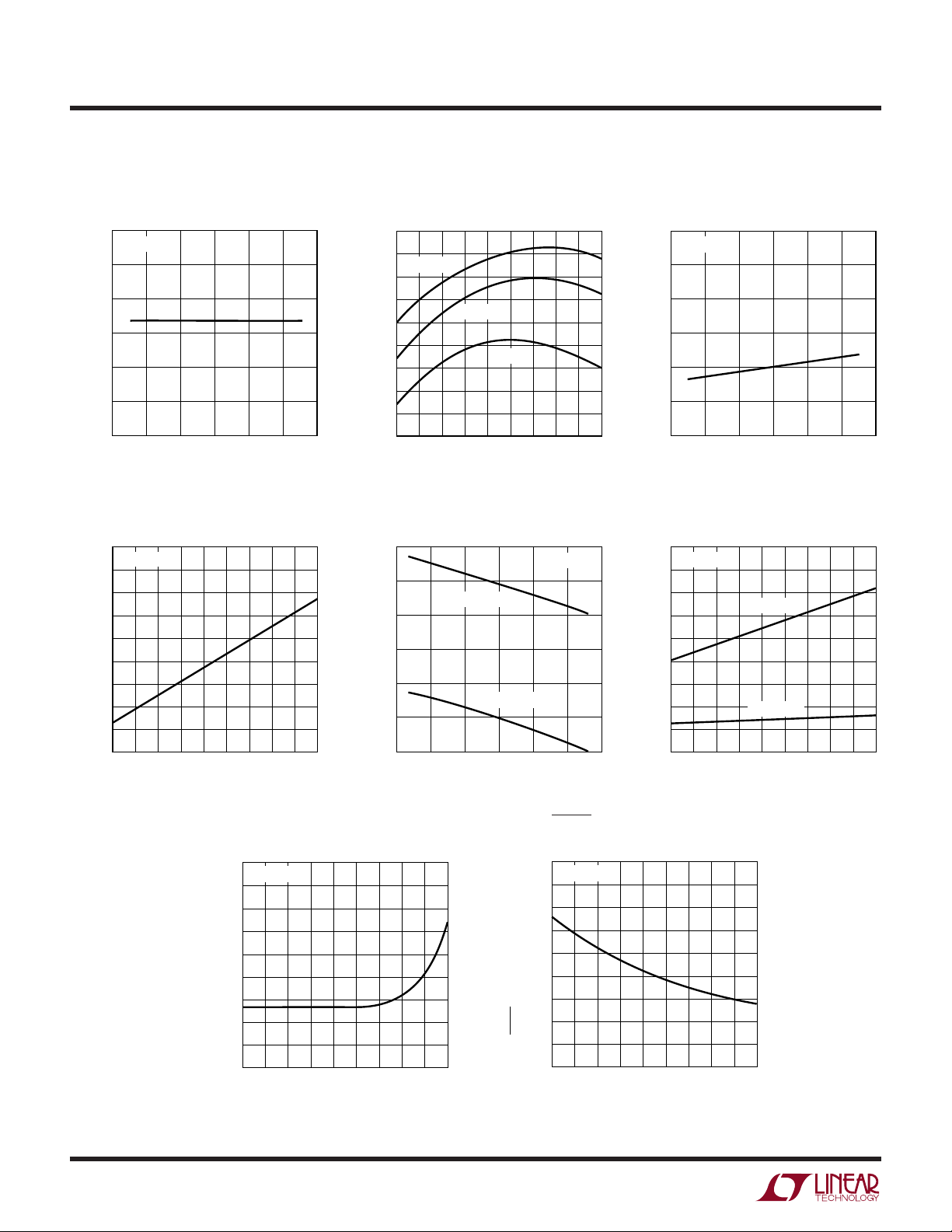
TIMER Threshold Voltage
vs Supply Voltage
1.244
TA = 25°C
1.242
1.240
1.238
1.236
1.234
TIMER THRESHOLD VOLTAGE (V)
1.232
2
2.45
VCC = 5V
2.40
2.35
2.30
2.25
2.20
2.15
TIMER CURRENT (µA)
2.10
2.05
2.00
–55
–35
6810
4
SUPPLY VOLTAGE (V)
5
–15
25
TEMPERATURE (°C)
TIMER Threshold Voltage
vs Temperature
1.242
12 14
1422 G10
1.241
1.240
1.239
1.238
1.237
1.236
1.235
TIMER THRESHOLD VOLTAGE (V)
1.234
1.233
–55
VCC = 12V
–35
–15
VCC = 5V
VCC = 3V
5
25
45
TEMPERATURE (°C)
65
125
85
105
1422 G11
ON Pin Threshold Voltage
vs Supply VoltageTIMER Current vs Temperature
1.32
1.30
2
HIGH THRESHOLD
LOW THRESHOLD
6810
4
SUPPLY VOLTAGE (V)
1.28
1.26
1.24
1.22
ON PIN THRESHOLD VOLTAGE (V)
45
65
125
85
105
1422 G13
1.20
TA = 25°C
12 14
1422 G14
TIMER Current vs Supply Voltage
2.6
TA = 25°C
2.5
2.4
2.3
2.2
TIMER CURRENT (µA)
2.1
2.0
2
6810
4
SUPPLY VOLTAGE (V)
ON Pin Threshold Voltage
vs Temperature
1.38
VCC = 5V
1.36
1.34
1.32
1.30
1.28
1.26
1.24
ON PIN THRESHOLD VOLTAGE (V)
1.22
1.20
–55
–35
INPUT HIGH
INPUT LOW
5
–15
25
TEMPERATURE (°C)
45
12 14
1422 G12
65
125
85
105
1422 G15
4
Current Limit Threshold
vs Temperature
85
VCC = 5V
80
75
70
65
60
55
50
CURRENT LIMIT THRESHOLD (mV)
45
40
–35
–55
5
–15
25
TEMPERATURE (°C)
45
RESET Pull-Up Current
vs Temperature
22
VCC = 5V
20
18
16
14
12
10
8
RESET PULL-UP CURRENT (µA)
6
4
–35
125
85
105
65
1422 G17
–55
5
–15
25
TEMPERATURE (°C)
45
65
125
85
105
1422 G18
Page 5
UW
TYPICAL PERFORMANCE CHARACTERISTICS
RESET Voltage vs Temperature
0.24
VCC = 5V
0.22
3mA PULL-UP
0.20
0.18
0.16
0.14
0.12
RESET VOLTAGE (V)
0.10
0.08
0.06
–55
–35
–15
5
25
45
TEMPERATURE (°C)
65
125
85
105
1422 G19
55
50
45
40
35
30
25
ON PIN PULSE TIME (µs)
20
15
10
UUU
PIN FUNCTIONS
ON Pin Pulse (Soft Reset) Time
vs Temperature
VCC = 3V
VCC = 5V
VCC = 12V
5
25
–55
–35
–15
TEMPERATURE (°C)
45
65
85
LTC1422
125
105
1422 G20
RESET (Pin 1) : Open drain output to GND with a 12µA
pull-up to VCC. This pin is pulled low when the voltage at
the FB (Pin 5) goes below the FB pin threshold. The RESET
pin will go high one timing cycle after the voltage at the FB
pin goes above the FB pin threshold. An external pull-up
resistor can be used to speed up the rising edge on the
RESET pin or pull the pin to a voltage higher or lower than
VCC.
ON (Pin 2): Analog Input Pin. The threshold is set at 1.30V
with 80mV hysteresis. When the ON pin is pulled high, the
timer turns on for one cycle, then the charge pump turns
on. When the ON pin is pulled low longer than 40µs, the
GATE pin will be pulled low and remain off until the ON pin
is pulled high.
If the ON pin is pulled low for less than 15µs a soft reset
will occur. The charge pump remains on, and the RESET
pin is pulled low for one timing cycle starting 30µs from
the falling edge of the ON pin.
The ON pin is also used to reset the electronic circuit
breaker. If the ON pin is cycled low and high following the
trip of the circuit breaker, the circuit breaker is reset and
a normal power-up sequence will occur.
TIMER (Pin 3): Analog system timing generator pin. This
pin is used to set the delay before the charge pump turns
on after the ON pin goes high. It also sets the delay before
the RESET pin goes high, after the output supply voltage
is good, as sensed by the FB pin.
When the timer is off, an internal N-channel shorts the
TIMER pin to ground. When the timer is turned on, a 2µA
current from VCC is connected to the TIMER pin and the
voltage starts to ramp up with a slope given by: dV/dt =
2µA/C
. When the voltage reaches the trip point
TIMER
(1.232V), the timer will be reset by pulling the TIMER pin
back to ground. The timer period is given by: (1.232V •
C
TIMER
)/2µA.
GND (Pin 4): Chip Ground.
FB (Pin 5): Analog comparator input used to monitor the
output supply voltage with an external resistive divider.
When the voltage on the FB pin is lower than the 1.232V,
the RESET pin will be pulled low. An internal filter helps
prevent negative voltage glitches from triggering a reset.
When the voltage on the FB pin rises above the trip point,
the RESET pin will go high after one timing cycle.
5
Page 6

LTC1422
UUU
PIN FUNCTIONS
GATE (Pin 6): The high side gate drive for the external
N-Channel. An internal charge pump guarantees at least
10V of gate drive. The slope of the voltage rise or fall at the
GATE is set by an external capacitor connected between
GATE and GND, and the 10µA charge pump output cur-
rent. When the circuit breaker trips, the undervoltage
lockout circuit monitoring V
trips, or the ON pin is pulled
CC
low for more than 40µs, the GATE pin is immediately
pulled to GND.
SENSE (Pin 7) : Circuit Breaker Set Pin. With a sense
resistor placed in the supply path between V
and SENSE,
CC
W
BLOCK DIAGRA
V
CC
8
SENSE
–
+
the circuit breaker will trip when the voltage across the
resistor exceeds 50mV for more than 10µs. If the circuit
breaker trip current is set to twice the normal operating
current, only 25mV is dropped across the sense resistor
during normal operation. To disable the circuit breaker,
V
and SENSE can be shorted together.
CC
V
(Pin 8): The positive supply input, ranging from 2.7V
CC
to 13.2V for normal operation. ICC is typically 0.6mA. An
undervoltage lockout circuit disables the chip until the
voltage at VCC is greater than 2.47V.
GATE
7
–
+
50mV
Q3
6
CHARGE
PUMP
ON
TIMER
COMP 3
2
3
Q1 Q2
REF
2µA
REF
+
–
+
–
COMP 1
COMP 4
2.47V
UVL
LOGIC
10µs
FILTER
1.232V
REFERENCE
GLITCH
FILTER
COMP 2
REF
–
12µA
1422 BD
5
FB
1
RESET
4
GND
+
6
Page 7

LTC1422
U
WUU
APPLICATIONS INFORMATION
Hot Circuit Insertion
When circuit boards are inserted into a live backplane, the
supply bypass capacitors on the board can draw huge
transient currents from the backplane power bus as they
charge up. The transient currents can cause permanent
damage to the connector pins and cause glitches on the
system supply, causing other boards in the system to
reset.
The LTC1422 is designed to turn a board’s supply voltage
on and off in a controlled manner, allowing the board to be
safely inserted or removed from a live backplane. The chip
also provides a system reset signal to indicate when board
supply voltage drops below a programmable voltage.
Power Supply Ramping
The onboard power supply is controlled by placing an
external N-channel pass transistor in the power path
(Figure 1). R1 provides current fault detection and R2
prevents high frequency oscillation. By ramping up the
gate of the pass transistor at a controlled rate, the transient
surge current (I = C • dV/dt) drawn from the main backplane
supply can be limited to a safe value when the board makes
connection.
VCC + 10V
V
SLOPE = 10µA/C1
CC
t
1
t
2
GATE
V
OUT
1422 F02
Figure 2. Supply Turn-On
equal to 10µA/C1 (Figure 2), where C1 is the external
capacitor connected between the GATE pin and GND.
The ramp time for the supply is equal to: t = (VCC • C1)/
10µA. After the ON pin has been pulled low for more than
40µs, the GATE is immediately pulled to GND.
Voltage Monitor
The LTC1422 uses a 1.232V bandgap reference, precision
voltage comparator and a resistive divider to monitor the
output supply voltage (Figure 3).
V
CC
R1
8
VCCSENSE
ON
TIMER GND
34
76
LTC1422
C2
Q1
GATE
RESET
FB
R2
10Ω
V
OUT
+
C
R3
C1
52
1
R4
LOAD
1422F01
Figure 1. Supply Control Circuitry
When power is first applied to the chip, the gate of the
N-channel (Pin 6) is pulled low. After the ON pin is held
high for at least one timing cycle, the charge pump is
turned on. The voltage at GATE begins to rise with a slope
ON
V
CC
2
LOGIC
R1
8
SENSE
V
CC
COMP 2
Q1
R2
C1
6
7
GATELTC1422
+
FB
R3
5
R4
V
OUT
+
C
LOAD
–
12µA
TIMER
34
C2
1.232V
REFERENCE
Q2
µP
1
RESET
1422 F03
Figure 3. Supply Monitor Block Diagram
7
Page 8

LTC1422
RESET
V
OUT
GATE
1422 F05
TIMER
ON
30µs
12
30µs
3465
15µs
20µs
U
WUU
APPLICATIONS INFORMATION
1234
V2 V2 V2V1V1
V
OUT
1.232V
TIMER
RESET
Figure 4. Supply Monitor Waveforms
When the voltage at the FB pin rises above its reset
threshold (1.232V), the comparator COMP 2 output goes
high, and a timing cycle starts (Figure 4, time points 1 and
4). After a complete timing cycle, RESET is pulled high.
The 12µA pull-up current source to VCC on RESET has a
series diode so the pin can be pulled above VCC by an
external pull-up resistor without forcing current back into
supply.
When the supply voltage at the FB pin drops below its reset
threshold, the comparator Comp 2 output goes low. After
passing through a glitch filter, RESET is pulled low (time
point 2). If the FB pin rises above the reset threshold for
less than a timing cycle, the RESET output will remain low
(time point 3).
1.232V
1422 F04
Figure 5. Soft Reset Waveforms
If the ON pin is held low for longer than 40µs, the gate will
turn off and the RESET pin will eventually go low (time
points 4, 5 and 6).
Timer
The system timing for the LTC1422 is generated by the
circuitry shown in Figure 6. The timer is used to set the
turn-on delay after the ON pin goes high and the delay
before the RESET pin goes high after the output supply
voltage is good as sensed by the FB pin.
Glitch Filter
The LTC1422 has a glitch filter to prevent RESET from
generating a system reset when there are transients on the
FB pin. The filter is 20µs for large transients (greater than
150mV) and up to 80µs for small transients. The relation-
ship between glitch filter time and the transient voltage is
shown in Typical Performance curve: Glitch Filter Time vs
Feedback Transient.
Soft Reset
In some cases a system reset is desired without a power
down. The ON pin can signal the RESET pin to go low
without turning off the external N-channel (a soft reset).
This is accomplished by holding the ON pin low for only
15µs or less (Figure 5, time point 1). At about 30µs from
the falling edge of the ON pin (time point 2) the RESET pin
goes low and stays low for one timing cycle.
ON
V
CC
2
2µA
R1
8
SENSE
V
CC
+
COMP 4
1.232V
TIMER
3
–
Q1
C2
7
LOGIC
Q2
R2
C1
6
GATELTC1422
5
SUPPLY
MONITOR
1
4
+
R3
R4
RESET
1422 F06
V
C
OUT
LOAD
Figure 6. System Timing Block Diagram
8
Page 9

LTC1422
U
WUU
APPLICATIONS INFORMATION
When the timer is off, the internal N-channel Q1 shorts the
TIMER pin to ground. When the timer is turned on, a 2µA
current from VCC is connected to the TIMER pin and the
voltage on the external capacitor C2 starts to ramp up with
a slope given by: dV/dt = 2µA/C2. When the voltage
reaches the trip point (1.232V), the timer will be reset by
pulling the TIMER pin back to ground. The timer period is
given by: (1.232V • C2)/2µA. For a 200ms delay, use a
0.33µF capacitor.
Electronic Circuit Breaker
The LTC1422 features an electronic circuit breaker function that protects against short circuits or excessive currents on the supply. By placing a sense resistor between
the supply input and SENSE pin, the circuit breaker will be
tripped whenever the voltage across the sense resistor is
greater than 50mV for more than 10µs. When the circuit
breaker trips, the GATE pin is immediately pulled to
ground and the external N-channel is quickly turned off.
When the ON pin is cycled off for greater than 40µs and
then on as shown in Figure 7, time point 7, the circuit
breaker is reset and another timing cycle is started.
At the end of the timer cycle (time point 8), the charge
pump will turn on again. If the circuit breaker feature is not
required, the SENSE pin should be shorted to VCC.
If more than 10µs of response time is needed to reject
supply noise, an external resistor and capacitor can be
added to the sense circuit as shown in Figure 8.
Connection Sense with ON Pin
The ON pin can be used to sense board connection to the
backplane as shown in Figure 9.
Using staggered connection pins, ground mates first to
discharge any static build up on the board, followed by the
VCC connection and all other pins. When VCC makes
connection, the bases of transistors Q3 and Q4 are pulled
high turning them on and pulling the ON pin to ground.
When the base connector pins of Q3 and Q4 finally mate
to the backplane, the bases are shorted to ground. This
turns off Q3 and Q4 and allows the ON pin to pull high and
start a power-up cycle. The base connection pins of Q3 and
Q4 should be located at opposite ends of the connector
1 2 3 4 5 6 7 8 9 10
V
CC
ON
V
– V
CC
SENSE
TIMER
GATE
V
OUT
RESET
1422 F07
Figure 7. Current Fault Timing
R1
C
F
8
SENSE
V
CC
LTC1422
Figure 8. Extending the Short-Circuit Protection Delay
Q1
R
F
R2
6
7
GATE
C1
1422 F08
because most people will rock the board back and forth to
get it seated properly.
A software-initiated power-down cycle can be started by
momentarily turning on transistor Q2, which will pull the
ON pin to ground. If the ON pin is held low for greater than
40µs, the GATE pin is pulled to ground. If the low pulse on
the ON pin is less than 15µs, a soft reset is generated.
Hot Swapping Two Supplies
With two external pass transistors, the LTC1422 can
switch two supplies. In some cases, it is necessary to bring
up the dominant supply first during power-up and ramp it
down last during the power-down phase. The circuit in
Figure 10 shows how to program two different delays for
the pass transistors. The 5V supply is powered up first. R1
9
Page 10

LTC1422
U
WUU
APPLICATIONS INFORMATION
V
CC
10k 10k
10k
CONNECTOR 1
ON/RESET
CONNECTOR 2
V
IN
3.3V
CURRENT LIMIT: 5A
V
IN
5V
RESET
ON
C1
0.33µF
16V
3.3V OUT
LTC1422
1
RESET
2
ON
3
TIMER
4
GND
5V OUT
SENSE
GATE
V
CC
FB
Q4
Q2: 2N7002LT1
Q3, Q4: MMBT3904LT1
8
7
6
5
R1
8
V
CC
ON
2
Q3
TIMER
Q2
+
COMP 5
REF
–
3
C2
Figure 9. ON Pin Circuitry
1/2 Si99436
R2
0.01Ω
5%
Q1
1/2 Si9436
R3
10Ω
5%
R1
10k
5%
C3
0.047µF
25V
D1
1N4148
R6
1M
5%
SENSE
Q2
7
R7
10Ω
5%
C2
0.022µF
25V
LOGIC
Q1
6
GATE
LTC1422
4
R2
5
FB
1
+
+
R4
2.74k
1%
TRIP POINT: 4.6V
R5
1k
1%
V
OUT
+
C
LOAD
C1
R3
R4
RESET
1422 F09
V
OUT
3.3V
C
LOAD
V
OUT
5V
C
LOAD
1422 F10
Figure 10. Switching 5V and 3.3V
and C3 are used to set the rise and fall delays on the 5V
supply. Next, the 3.3V supply ramps up with a 20ms delay
set by R6 and C2. On the falling edge, the 3.3V supply
ramps down first because R6 is bypassed by the diode D1.
Using the LTC1422 as a Linear Regulator
The LTC1422 can be used to Hot Swap the primary supply
and generate a secondary low dropout regulated supply.
Figure 11 shows how to switch a 5V supply and create a
3.3V supply using the reset comparator and one additional transistor. The FB pin is used to monitor the 3.3V
output. When the voltage on the gate of Q2 increases, the
3.3V increases. At the 3.3V threshold, the reset comparator will trip. The RESET pin goes high which turns on Q3.
This lowers the voltage on the gate of Q2. This feedback
loop is compensated by the capacitor C1 and the resistors
R6 and R7.
Hot Swapping 48V DC/DC Module with
Active Low On/Off Control Signal
Using a 7.5V Zener and a resistor, the LTC1422 can switch
supplies much greater than the 12V VCC pin rating. As
shown in Figure 12, the switching FET Q1 is connected as
a common source driver rather than the usual source
follower used in previous applications. This allows the
ground of the LTC1422 to sit at the negative terminal of the
48V input. The clamp circuit of R5 and D1 provides power
to the LTC1422. The resistive divider R1 and R2 at the ON
pin monitors the input supply. The switching FET Q1 is
prevented from turning on until the input supply is at least
38V. Using the reset comparator to monitor the gate
voltage allows the module to be turned on after the gate
has reached a minimum level plus one timing cycle. A high
voltage transistor Q2 is used to translate the RESET signal
to the module On/Off input.
10
Page 11

LTC1422
U
WUU
APPLICATIONS INFORMATION
Since the pass transistor is in a common source configuration, care must be taken to limit the inrush current into
capacitor C3. One way is to precharge C3 using resistor
R4. As the input supply is ramping up, current is flowing
through R4 and charging the capacitor C3. Once the input
supply crosses 38V, there is a timing cycle followed by the
ramp-up of the GATE pin. By this time the capacitor C3 is
sufficiently charged, thereby limiting the inrush current.
Another method to limit the inrush current is to slow down
the ramp-up rate of the GATE pin.
Hot Swapping 48V DC/DC Module with
Active High On/Off Control Signal
This application is identical to the previous except for the
polarity of the module’s on/off signal. The polarity reversal
is accomplished by transistor Q3 in Figure 13.
Hot Swapping Redundant 48V
In critical situations, redundant input supplies are necessary. In Figure 14 a redundant 48V input is switched to a
power module. Supplies 1 and 2 are wire OR’ed using two
diodes D2 and D3. This results in the most negative of
these two supplies being used to drive the power module.
If one of the supplies is disconnected or a fuse opens, the
fault signal will be activated via diodes D4 and D5 and the
reset comparator at the FB pin. The GATE IN signal on the
Vicor module is controlled using the high voltage PNP Q2.
Once the module’s minus input pin is more negative than
the base of Q2 plus a diode drop, Q2 will turn off and the
module will turn on. This occurs when the source of Q1
plus a Zener voltage (D1) is more positive than the drain
of Q1 (in other words, when the switching FET Q1 has only
7.5V across its drain source).
Hot Swapping 48V Module with Isolated Controller
A power supervisory controller will sometimes reside on
an isolated supply with responsibility for other supplies.
Figure 15 shows how to Hot Swap a controller’s 5V supply
and a 48V module using two LTC1422s. Assuming the 5V
supply comes up first, the controller waits for a power
good signal from the 48V circuit. Once it receives the right
signals the controller activates the GATE IN pin of the Vicor
power module.
Power Supply Sequencer
A circuit that forces two supply voltages to power up
together is shown in Figure 16. The input supply voltages
may power up in any sequence, but both input voltages
must be within tolerance before Q1 and Q2 turn on. Backto-back transistors Q1 and Q2 ensure isolation between
the two supplies.
When the 5V input powers up before 3.3V, Q1 and Q2
remain off and the 5V output remains off until the 3.3V
input is within tolerance as sensed by resistors R1 and R2.
When the 3.3V input powers up before 5V, the diode D1
will pull up the 5V supply output with it. Once the 5V input
powers up and is within tolerance as sensed by R4 and R5,
Q1 and Q2 will turn on in about 1ms and pull the 5V output
up to its final voltage.
CURRENT LIMIT: 2.5A
V
IN
5V
1
RESET
2
ON
3
TIMER
4
GND
Q2
MMFT2N02ELT1
LTC1422
SENSE
V
GATE
R1
0.02Ω
5%
8
CC
7
6
5
FB
Q1
MMFT2N02ELT1
R3
10Ω
5%
C2
0.1µF
16V
R6
1.6M
5%
R2
10Ω
5%
C1
0.0033µF
16V
Figure 11. Switching 5V and Generating 3.3V
R7
360k
5%
Q3
PN2222
+
+
R4
2.74k
1%
R5
1.62k
1%
C
C
LOAD
LOAD
C3
0.1µF
16V
1422 F11
V
OUT
3.3V
V
OUT
5V
11
Page 12

LTC1422
U
WUU
APPLICATIONS INFORMATION
Power N-Channel and Sense Resistor Selection
The decision of which external power N-Channel to use is
dependent on its maximum current rating and the maximum allowed current times R
drop across the
DS(ON)
transistor. Table 1 lists some transistors that are available.
Table 1. N-Channel Selection Guide
CURRENT LEVEL (A) PART NUMBER DESCRIPTION MANUFACTURER
0 to 2 MMDF3N02HD Dual N-Channel SO-8 ON Semiconductor
2 to 5 MMSF5N02HD Single N-Channel SO-8 ON Semiconductor
5 to 10 MTB50N06V Single N-Channel DD Pak ON Semiconductor
10 to 20 MTB75N05HD Single N-Channel DD Pak ON Semiconductor
Table 2. Sense Resistor Selection Guide
CURRENT LIMIT VALUE PART NUMBER DESCRIPTION MANUFACTURER
1A LR120601R050 0.05Ω 0.25W 1% Resistor IRC-TT
2A LR120601R025 0.025Ω 0.25W 1% Resistor IRC-TT
2.5A LR120601R020 0.02Ω 0.25W 1% Resistor IRC-TT
3.3A WSL2512R015F 0.015Ω 1W 1% Resistor Vishay-Dale
5A LR120601R010 0.01Ω 0.25W 1% Resistor IRC-TT
10A WSR2R005F 0.005Ω 2W 1% Resistor Vishay-Dale
Table 2 lists some current sense resistors that can be
used with the circuit breaker. Since this information is
subject to change, please verify the part numbers with the
manufacturer. Table 3 lists the web sites of several manufacturers.
= 0.1Ω
R
DS(ON)
= 0.025Ω
R
DS(ON)
= 0.028Ω
R
DS(ON)
R
= 0.0095Ω
DS(ON)
Table 3. Manufacturers’ Web Sites
MANUFACTURER WEB SITE
TEMIC Semiconductor www.temic.com
International Rectifier www.irf.com
ON Semiconductor www.onsemiconductor.com
Harris Semiconductor www.semi.harris.com
IRC-TT www.irctt.com
Vishay-Dale www.vishay.com
12
Page 13

LTC1422
U
WUU
APPLICATIONS INFORMATION
R1
36k
5%
48V
+
–
FUSE
MMBT5551LT1
R2
1.2k
5%
Q2
C1
0.47µF
25V
CIRCUIT TURNS ON WHEN V
CIRCUIT FOR ACTIVE LOW TURN-ON MODULES
1
2
3
4
LTC1422
RESET
ON
TIMER
GND
V
SENSE
GATE
CC
FB
IN
8
7
6
5
> 38V
R5
10k
5%
D1
7.5V
1N755A
C4
1µF
25V
R6
1M
5%
R7
270k
5%
C2
0.1µF
25V
OPTIONAL
PRECHARGE RESISTOR
100µF
100V
Q1
IRF530
R4
510Ω
5%
C3
R3
10Ω
5%
AT&T
JW050A1-E
50W
+
+
V
V
OUT
+
IN
V
IN
SENSE
SENSE
–
ON/OFF
+
–
–
V
OUT
5V
1422 F12
+
48V
–
FUSE
R1
36k
5%
MMBT5551LT1
R2
1.2k
5%
Figure 12. Switching 48V to an AT&T Module
++
+
C3
100µF
C2
0.1µF
25V
Q1
IRF530
R8
510Ω
5%
100V
R3
10Ω
5%
R5
10k
5%
LTC1422
Q2
1
RESET
2
ON
3
TIMER
4
GND
C1
0.1µF
25V
CIRCUIT TURNS ON WHEN V
CIRCUIT FOR ACTIVE HIGH TURN-ON MODULES
V
SENSE
GATE
8
CC
7
6
5
FB
D1
7.5V
1N755A
> 38V
IN
C4
1µF
25V
R6
1M
5%
R7
270k
5%
VICOR
VI-J30-CY
__
GATE IN
R4
5.1k
5%
Q3
MMBT5551LT1
5V
PRECHARGE RESISTOR
Figure 13. Switching 48V to a Vicor Module
OPTIONAL
1422 F13
13
Page 14

LTC1422
U
WUU
APPLICATIONS INFORMATION
COMMON
RETURN
–48V
–48V
FUSE 1
FUSE 2
R6
10k
5%
R7
10k
5%
MUR415
MUR415
D4
1N4148
D5
1N4148
D2
D3
R1
36k
5%
R2
1.2k
5%
R10
5.1k
5%
FAULT
4N25
Figure 14. Hop Swapping Redundant 48V Supplies
R5
10k
5%
LTC1422
1
RESET
2
ON
3
TIMER
4
GND
C1
0.33µF
16V
Q1 TURNS ON WHEN V
FAULT GOES LOW WHEN EITHER SUPPLY FAILS
V
SENSE
GATE
IN
CC
FB
> 38V
8
7
6
5
R9
1k
5%
D1
7.5V
1N755A
C3
+
100µF
100V
R4
10k
5%
C2
0.1µF
25V
C4
1µF
25V
Q1
IRF530
R8
510Ω
5%
OPTIONAL
PRECHARGE RESISTOR
++
VICOR
VI-J30-CY
__
GATE IN
Q2
MPSA56
R3
10Ω
5%
5V
1422 F14
48V
5V
C5
0.33µF
16V
R1
36k
5%
R4
4N25
5.1k
5%
1
2
3
4
C1
0.1µF
25V
CIRCUIT TURNS ON WHEN V
CIRCUIT FOR ACTIVE HIGH TURN-ON MODULES
+
–
R2
1.2k
5%
FUSE
1
2
3
4
LTC1422
RESET
ON
TIMER
GND
LTC1422
RESET
ON
TIMER
GND
SENSE
V
GATE
SENSE
GATE
CC
FB
V
8
7
6
5
IN
CC
FB
> 38V
8
7
6
5
R5
6.2k
5%
0.5Ω
D1
7.5V
1N755A
R9
5%
C4
1µF
25V
Q4
R10
10Ω
5%
C6
0.022µF
16V
R13
28k
1%
R14
10k
1%
R6
1M
5%
R7
270k
5%
C2
0.1µF
25V
OPTIONAL
PRECHARGE RESISTOR
+
100µF
IRF530
R8
510Ω
5%
100V
Q1
C7
47µF
16V
C3
R3
10Ω
5%
RESET
++
+
__
4N25
V
CC
µP
PWRGD
GND
VICOR
VI-J30-CY
GATE IN
1422 F15
ON
R11
R12
5.1k
5.1k
5%
5%
5V
Figure 15. Switching 48V to a Vicor Module with Isolated Controller
14
Page 15

LTC1422
U
WUU
APPLICATIONS INFORMATION
V
IN
3.3V
V
IN
5V
R1
1.3k
1
2
3
4
RESET
ON
LTC1422
TIMER
GND
1%
R2
1 k
1%
Figure 16. Power Supply Sequencer
U
PACKAGE DESCRIPTION
0.300 – 0.325
(7.620 – 8.255)
Dimensions in inches (millimeters) unless otherwise noted.
8-Lead PDIP (Narrow 0.300)
0.045 – 0.065
(1.143 – 1.651)
Q1
1/2
MMDF 2N02E
8
V
CC
7
SENSE
GATE
FB
R4
2.74k
1%
6
5
R5
1k
1%
N8 Package
(LTC DWG # 05-08-1510)
0.130 ± 0.005
(3.302 ± 0.127)
R3
10Ω
5%
C1
0.047µF
25V
Q1
1/2
MMDF 2N02E
V
OUT
3.3V
D1
MBRS120T3
V
OUT
5V
1422 F16
876
0.400*
(10.160)
MAX
5
0.065
(1.651)
0.009 – 0.015
(0.229 – 0.381)
+0.035
0.325
–0.015
+0.889
8.255
()
–0.381
*THESE DIMENSIONS DO NOT INCLUDE MOLD FLASH OR PROTRUSIONS.
MOLD FLASH OR PROTRUSIONS SHALL NOT EXCEED 0.010 INCH (0.254mm)
TYP
0.100
(2.54)
BSC
8-Lead Plastic Small Outline (Narrow 0.150)
0.010 – 0.020
(0.254 – 0.508)
0.008 – 0.010
(0.203 – 0.254)
*
DIMENSION DOES NOT INCLUDE MOLD FLASH. MOLD FLASH
SHALL NOT EXCEED 0.006" (0.152mm) PER SIDE
**
DIMENSION DOES NOT INCLUDE INTERLEAD FLASH. INTERLEAD
FLASH SHALL NOT EXCEED 0.010" (0.254mm) PER SIDE
× 45°
0.016 – 0.050
(0.406 – 1.270)
0.053 – 0.069
(1.346 – 1.752)
0°– 8° TYP
0.014 – 0.019
(0.355 – 0.483)
TYP
0.125
(3.175)
MIN
0.018 ± 0.003
(0.457 ± 0.076)
S8 Package
(LTC DWG # 05-08-1610)
0.004 – 0.010
(0.101 – 0.254)
0.050
(1.270)
BSC
0.020
(0.508)
MIN
0.228 – 0.244
(5.791 – 6.197)
0.255 ± 0.015*
(6.477 ± 0.381)
0.189 – 0.197*
(4.801 – 5.004)
7
8
1
2
12
6
3
4
3
N8 1098
5
0.150 – 0.157**
(3.810 – 3.988)
4
SO8 1298
Information furnished by Linear Technology Corporation is believed to be accurate and reliable.
However, no responsibility is assumed for its use. Linear Technology Corporation makes no representation that the interconnection of its circuits as described herein will not infringe on existing patent rights.
15
Page 16

LTC1422
TYPICAL APPLICATION
U
Current Sensing with 48V Applications
In the LTC1422, the SENSE pin threshold is 50mV below
the VCC pin. Typically, the current sense resistor is connected to the VCC pin, but in 48V applications the sense
resistor is connected to the negative terminal of the 48V
supply. The circuit in Figure 17 translates the current in the
sense resistor to a resistor connected to the LTC1422
SENSE pin.
The voltage drop across the current sense resistor R
is proportional to the load current I
across R
forced on R
+
48V
–
is buffered by the op amp follower and is
SENSE
R1
36k
5%
R2
1.2k
5%
.
LTC1422
1
RESET
2
ON
3
TIMER
4
GND
C1
0.47µF
25V
MIRROR
FUSE
. The voltage drop
LOAD
R5
15k
5%
8
V
CC
7
SENSE
6
GATE
5
FB
D1
7.5V
1N755A
I
MIRROR
VN2222L
I
MIRROR
Q2
SENSE
R
TRIP
10Ω
5%
R
MIRROR
39Ω
5%
The mirror current can be described as: I
R
SENSE/RMIRROR
trip resistor R
50mV across R
low (50mV = I
R
). This example uses a 48V input but this translation
TRIP
. The mirror current flows through the
. When the mirror current generates
TRIP
, the LTC1422 will latch the GATE pin
TRIP
MIRROR
• R
TRIP
= I
LOAD
MIRROR
• R
SENSE/RMIRROR
= I
LOAD
•
•
circuit can be used anywhere the current sense resistor is
not tied to VCC.
Q1
IRF530
R
SENSE
0.02Ω
5%
I
LOAD
1422 F17
+
LOAD
–
C4
1µF
25V
7
LT1006
4
+
–
OPAMP
C5
0.22µF
100V
+
R4
10k
5%
R6
1M
5%
R7
270k
5%
3
2
C2
0.1µF
25V
R3
10Ω
5%
100µF
100V
+
C3
Figure 17. Switching 48V with Current Sensing
RELATED PARTS
PART NUMBER DESCRIPTION COMMENTS
LTC1421 Hot Swap Controller 24-Pin Multiple Supplies
LT1640L/LT1640H Negative Voltage Hot Swap Controller in SO-8 Operates from –10V to –80V
LT1641 High Voltage Hot Swap Controller in SO-8 Operates from 9V to 80V
LT1642 Fault Protected Hot Swap Controller Operates Up to 16.5V, Protected to 33V
LTC1643L/LTC1643H PCI-Bus Hot Swap Controller 3.3V, 5V and ±12V in Narrow 16-Pin SSOP
LT1645 2-Channel Hot Swap Controller Operates from 1.2V to 12V, Power Sequencing
LTC1647 Dual Hot Swap Controller in SO-8 or SSOP-16 Two ON Pins, Operates from 2.7V to 16.5V
1422fa LT/TP 0300 2K REV A • PRINTED IN USA
LINEAR TECHNOLOGY CORPORATION 1997
16
Linear Technology Corporation
1630 McCarthy Blvd., Milpitas, CA 95035-7417
(408) 432-1900 ● FAX: (408) 434-0507
●
www.linear-tech.com
 Loading...