

Page 1
FEATURES
INPUT FREQUENCY (Hz)
4
EFFECTIVE BITS
S/(N + D) (dB)
6
8
10
12
10k 100k 1M
1417 TA02
2
1k
14 86
80
74
68
62
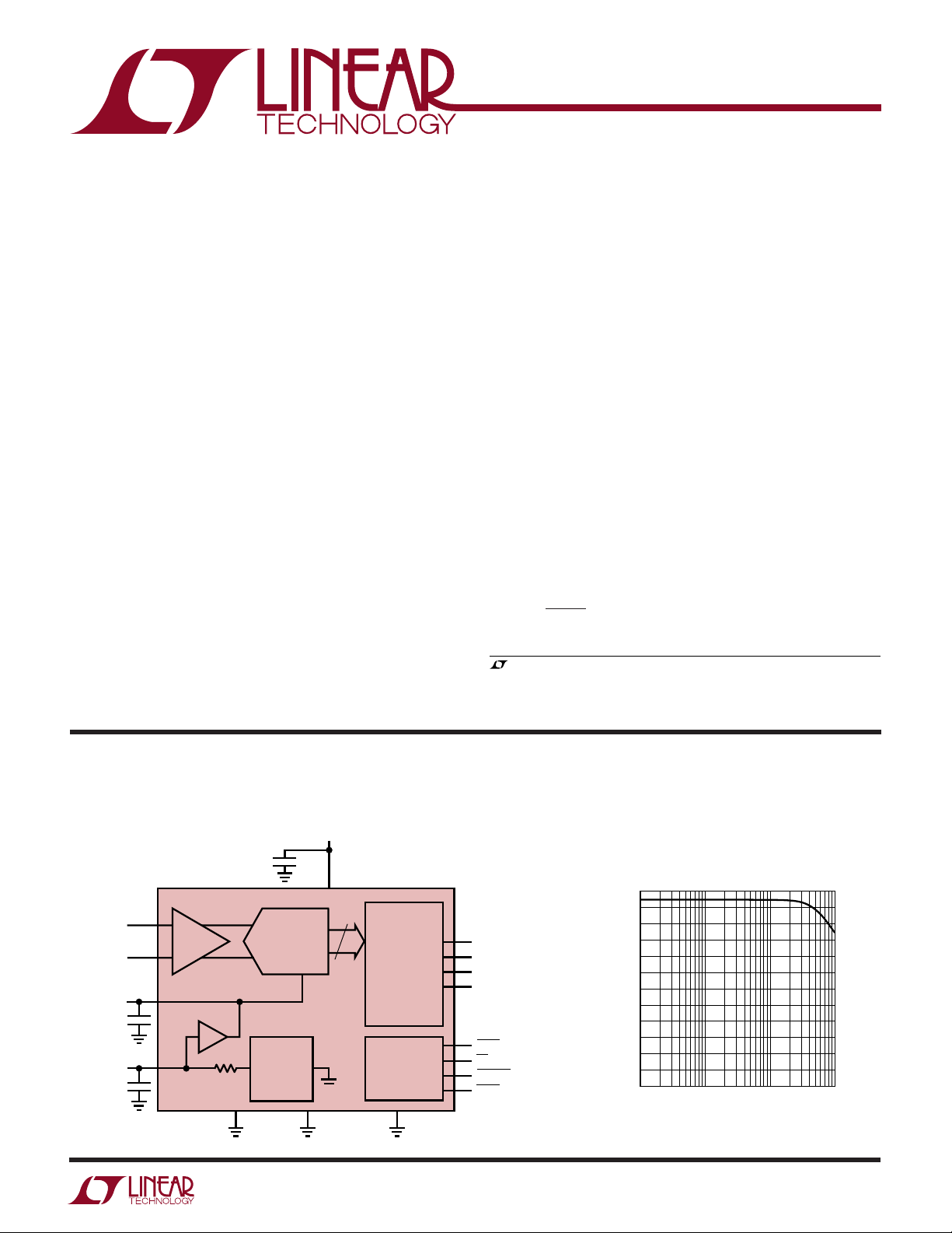
LTC1417
Low Power 14-Bit, 400ksps
Sampling ADC Converter
with Serial I/O
U
DESCRIPTIO
■
16-Pin Narrow SSOP Package (SO-8 Footprint)
■
Sample Rate: 400ksps
■
±1.25LSB INL and ±1LSB DNL Max
■
Power Dissipation: 20mW (Typ)
■
Single Supply 5V or ±5V Operation
■
Serial Data Output
■
No Missing Codes Over Temperature
■
Power Shutdown: Nap and Sleep
■
External or Internal Reference
■
Differential High Impedance Analog Input
■
Input Range: 0V to 4.096V or ±2.048V
■
81dB S/(N + D) and –95dB THD at Nyquist
U
APPLICATIO S
■
High Speed Data Acquisition
■
Digital Signal Processing
■
Isolated Data Acquisition Systems
■
Audio and Telecom Processing
■
Spectrum Instrumentation
The LTC®1417 is a low power, 400ksps, 14-bit A/D converter. This versatile device can operate from a single 5V or
±5V supplies. An onboard high performance sample-andhold, a precision reference and internal trimming minimize
external circuitry requirements. The low 20mW power
dissipation is made even more attractive with two userselectable power shutdown modes.
The LTC1417 converts 0V to 4.096V unipolar inputs when
using a 5V supply and ±2.048V bipolar inputs when using
±5V supplies. DC specs include ±1.25LSB INL, ±1LSB
DNL and no missing codes over temperature. Outstanding
AC performance includes 81dB S/(N + D) and 95dB THD
at a Nyquist input frequency of 200kHz.
The internal clock is trimmed for 2µs maximum conver-
sion time. A separate convert start input and a data ready
signal (BUSY) ease connections to FIFOs, DSPs and
microprocessors.
, LTC and LT are registered trademarks of Linear Technology Corporation.
U
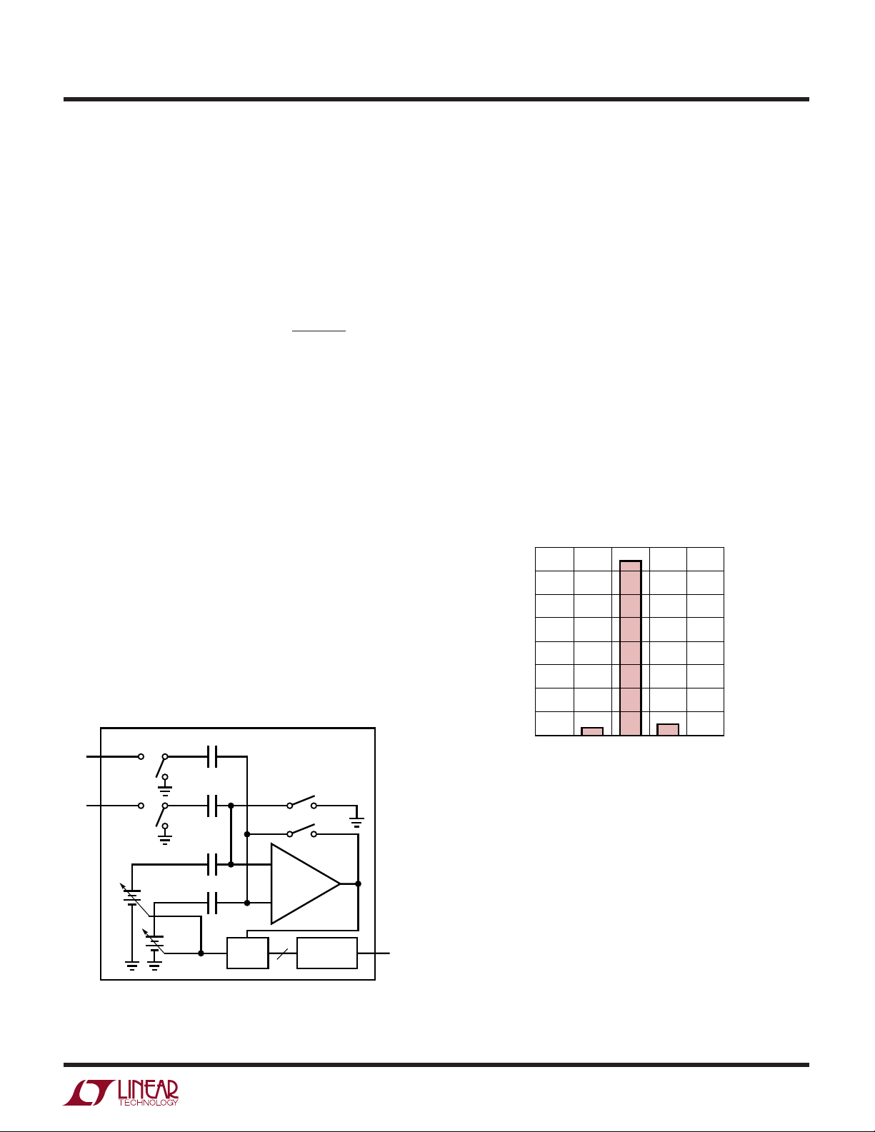
EQUIVALE T BLOCK DIAGRA
A 400kHz, 14-Bit Sampling A/D Converter in a Narrow 16-Lead SSOP Package
LTC1417
1
+
A
IN
–
A
IN
REFCOMP
10µF
V
REF
1µF
S/H
2
4
BUFFER
3
4.096V
8k
REFERENCE
AGND
10µF
14-BIT ADC
2.5V
5V
VDD16
14
V
SS
(0V OR –5V)
SERIAL
PORT
TIMING AND
LOGIC
DGND10155
W
6
7
8
9
14
12
13
11
1417 TA01
EXTCLKIN
SCLK
CLKOUT
D
OUT
BUSY
RD
CONVST
SHDN
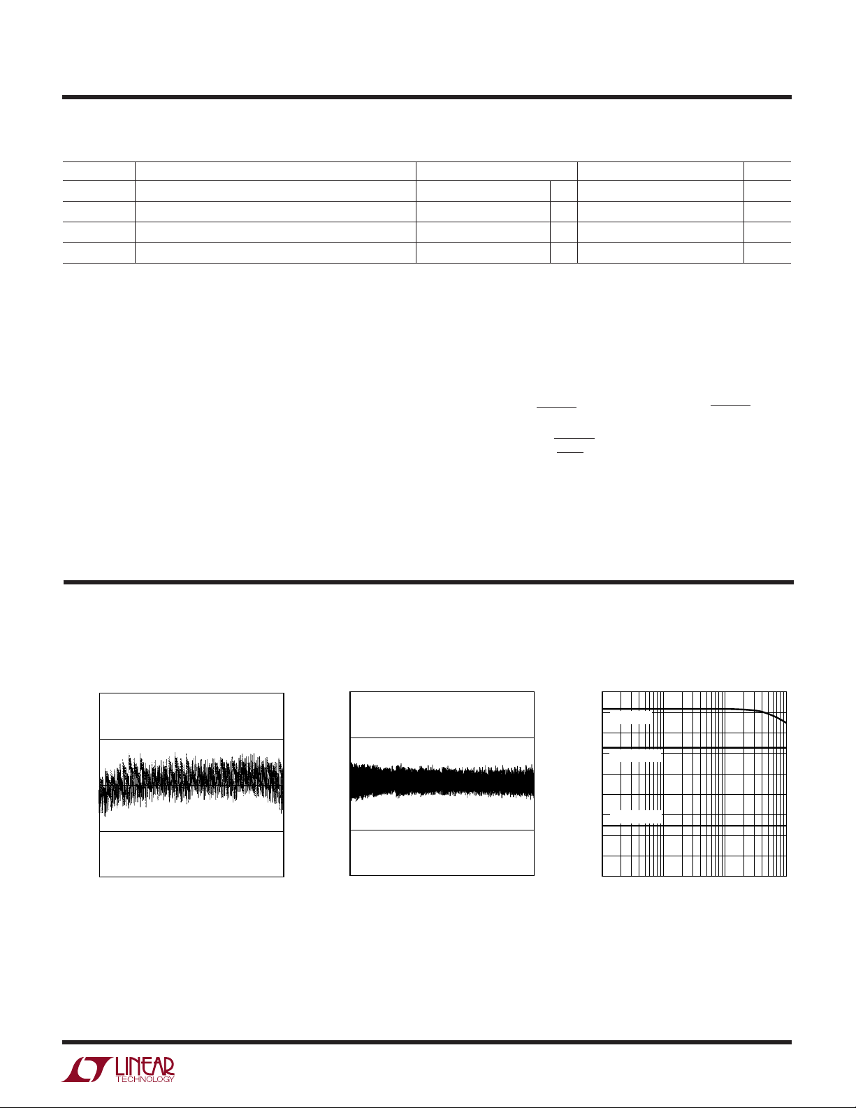
Effective Bits and Signal-to-(Noise + Distortion)
vs Input Frequency
1
Page 2
LTC1417
O
A
S
(Notes 1, 2)
W
LUTEXI TIS
A
WUW
U
ARB
G
Positive Supply Voltage (VDD) .................................. 6V
Negative Supply Voltage (VSS)
Bipolar Operation Only .......................... –6V to GND
Total Supply Voltage (VDD to VSS)
Bipolar Operation Only ....................................... 12V
Analog Input Voltage (Note 3)
Unipolar Operation .................. – 0.3V to (VDD + 0.3V)
Bipolar Operation............ (VSS – 0.3) to (VDD + 0.3V)
Digital Input Voltage (Note 4)
Unipolar Operation ............................... –0.3V to 10V
Bipolar Operation.........................(VSS – 0.3V) to 10V
Digital Output Voltage
Unipolar Operation ................... –0.3 to (VDD + 0.3V)
Bipolar Operation........... (VSS – 0.3V) to (VDD + 0.3V)
Power Dissipation............................................. 500mW
Operating Temperature Range
LTC1417C .............................................. 0°C to 70°C
LTC1417I............................................ –40°C to 85°C
Storage Temperature Range ................ –65°C to 150°C
Lead Temperature (Soldering, 10 sec)................. 300°C
/
PACKAGE
+
1
A
IN
–
2
A
IN
3
V
REF
REFCOMP
EXTCLKIN
CLKOUT
Consult factory for Military grade parts.
4
5
AGND
6
7
SCLK
8
16-LEAD (NARROW) PLASTIC SSOP
T
JMAX
O
RDER I FOR ATIO
TOP VIEW
16
15
14
13
12
11
10
9
GN PACKAGE
= 110°C, θJA = 95°C/W
V
DD
V
SS
BUSY
CONVST
RD
SHDN
DGND
D
OUT
WU
ORDER
PART NUMBER
LTC1417ACGN
LTC1417CGN
LTC1417AIGN
LTC1417IGN
GN PART MARKING
1417A
1417
1417AI
1417I
U
U
CO
temperature range, otherwise specifications are at TA = 25°C. Specifications are measured while using the internal reference unless
otherwise noted. (Notes 5, 6)
PARAMETER CONDITIONS MIN TYP MAX MIN TYP MAX UNITS
Resolution ● 14 14 Bits
No Missing Codes ● 13 14 Bits
Integral Linearity Error (Note 7) ● ±0.8 ±2 ±0.5 ±1.25 LSB
Differential Linearity Error ● ±0.7 ±1.5 ±0.35 ±1 LSB
Transition Noise (Note 12) 0.33 0.33 LSB
Offset Error External Reference (Note 8) ● ±5 ±20 ±2 ±10 LSB
Full-Scale Error Internal Reference ±15 ±60 ±15 ±60 LSB
Full-Scale Tempco I
VERTER
CCHARA TERIST
External Reference = 2.5V ±5 ±30 ±5 ±15 LSB
= 0, Internal Reference, 0°C ≤ TA ≤ 70°C ±15 ±10 ppm/°C
OUT(REF)
= 0, Internal Reference, –40°C ≤ TA ≤ 85°C ±20 ppm/°C
I
OUT(REF)
I
= 0, External Reference ±5 ±1 ppm/°C
OUT(REF)
ICS
The ● indicates specifications which apply over the full operating
LTC1417 LTC1417A
RMS
UU
A ALOG I PUT
otherwise specifications are at TA = 25°C. (Note 5)
SYMBOL PARAMETER CONDITIONS MIN TYP MAX UNITS
V
IN
I
IN
Analog Input Range (Note 9) 4.75V ≤ VDD ≤ 5.25V (Unipolar) ● 0 to 4.096 V
Analog Input Leakage Current CONVST = High ● ±1 µA
The ● indicates specifications which apply over the full operating temperature range,
4.75V ≤ V
≤ 5.25V, –5.25V ≤ VSS ≤ –4.75V (Bipolar) ● ±2.048 V
DD
2
Page 3
LTC1417
UU
A ALOG I PUT
otherwise specifications are at TA = 25°C. (Note 5)
SYMBOL PARAMETER CONDITIONS MIN TYP MAX UNITS
C
IN
t
ACQ
t
AP
t
jitter
CMRR Analog Input Common Mode Rejection Ratio 0V < (A
Analog Input Capacitance Between Conversions (Sample Mode) 14 pF
Sample-and-Hold Acquisition Time ● 150 500 ns
Sample-and-Hold Aperture Time –1.5 ns
Sample-and-Hold Aperture Time Jitter 5 ps
The ● indicates specifications which apply over the full operating temperature range,
During Conversions (Hold Mode) 3 pF
+
–
= A
IN
–2.048V < (A
) < 4.096V (Unipolar) 65 dB
IN
+
–
= A
IN
) < 2.048V (Bipolar) 65 dB
IN
RMS
UW
DY A IC ACCURACY
otherwise specifications are at TA = 25°C. (Note 5)
SYMBOL PARAMETER CONDITIONS MIN TYP MAX UNITS
S/(N + D) Signal-to-(Noise + Distortion) Ratio 100kHz Input Signal ● 79 81 dB
THD Total Harmonic Distortion 100kHz Input Signal, First Five Harmonics ● –85 –95 dB
SFDR Spurious Free Dynamic Range 200kHz Input Signal –98 dB
IMD Intermodulation Distortion f
Full Power Bandwidth 10 MHz
Full Linear Bandwidth S/(N + D) ≥ 77dB 0.8 MHz
The ● indicates specifications which apply over the full operating temperature range,
= 97.3kHz, f
IN1
= 104.6kHz –97 dB
IN2
UU U
I TER AL REFERE CE CHARACTERISTICS
operating temperature range, otherwise specifications are at TA = 25°C. (Note 5)
The ● indicates specifications which apply over the full
PARAMETER CONDITIONS MIN TYP MAX UNITS
V
Output Voltage I
REF
V
Output Tempco I
REF
V
Line Regulation 4.75V ≤ VDD ≤ 5.25V 0.05 LSB/V
REF
V
Output Resistance 0.1mA ≤ |I
REF
= 0 ● 2.480 2.500 2.520 V
OUT
= 0, 0°C ≤ TA ≤ 70°C ±10 ppm/°C
OUT
= 0, –40°C ≤ TA ≤ 85°C ±20 ppm/°C
I
OUT
–5.25V ≤ V
≤ –4.75V 0.05 LSB/V
SS
| ≤ 0.1mA 8 kΩ
OUT
UU
DIGITAL I PUTS A D DIGITAL OUTPUTS
operating temperature range, otherwise specifications are at TA = 25°C. (Note 5)
SYMBOL PARAMETER CONDITIONS MIN TYP MAX UNITS
V
IH
V
IL
I
IN
C
IN
V
OH
V
OL
I
OZ
C
OZ
I
SOURCE
I
SINK
High Level Input Voltage V
Low Level Input Voltage VDD = 4.75V ● 0.8 V
Digital Input Current VIN = 0V to V
Digital Input Capacitance 1.4 pF
High Level Output Voltage VDD = 4.75V, IO = –10µA 4.74 V
Low Level Output Voltage VDD = 4.75V, IO = 160µA 0.05 V
High-Z Output Leakage D
High-Z Output Capacitance D
Output Source Current V
Output Sink Current V
, CLKOUT V
OUT
, CLKOUT RD High (Note 9) ● 15 pF
OUT
= 5.25V ● 2.4 V
DD
DD
VDD = 4.75V, IO = –200µA ● 4.0 V
VDD = 4.75V, IO = –1.6mA ● 0.10 0.4 V
= 0V to VDD, RD High ● ±10 µA
OUT
= 0V –10 mA
OUT
= V
OUT
DD
The ● indicates specifications which apply over the full
● ±10 µA
10 mA
3
Page 4
LTC1417
WU
POWER REQUIRE E TS
otherwise specifications are at TA = 25°C. (Note 5)
SYMBOL PARAMETER CONDITIONS MIN TYP MAX UNITS
V
DD
V
SS
I
DD
I
SS
P
DIS
Positive Supply Voltage (Notes 10, 11) 4.75 5.25 V
Negative Supply Voltage (Note 10) Bipolar Only (VSS = 0V for Unipolar) – 4.75 –5.25 V
Positive Supply Current Unipolar, RD High (Note 5) ● 4.0 5.5 mA
Nap Mode SHDN = 0V, RD = 0V 750 µA
Sleep Mode SHDN = 0V, RD = 5V 0.1 µA
Negative Supply Current Bipolar, RD High (Note 5) ● 2.0 2.8 mA
Nap Mode SHDN = 0V, RD = 0V 0.7 µA
Sleep Mode SHDN = 0V, RD = 5V 1.5 nA
Power Dissipation Unipolar ● 20.0 27.5 mW
The ● indicates specifications which apply over the full operating temperature range,
Bipolar, RD High (Note 5)
Bipolar
● 4.3 6.0 mA
● 31.5 44 mW
UW
TI I G CHARACTERISTICS
range, otherwise specifications are at TA = 25°C. (Note 5)
SYMBOL PARAMETER CONDITIONS MIN TYP MAX UNITS
f
SAMPLE(MAX)
t
CONV
t
ACQ
t
+ t
ACQ
CONV
t
1
t
2
t
3
t
4
t
5
t
6
t
7
t
8
t
9
t
10
t
11
t
12
f
SCLK
f
EXTCLKIN
t
dEXTCLKIN
Maximum Sampling Frequency ● 400 kHz
Conversion Time ● 1.8 2.25 µs
Acquisition Time ● 150 500 ns
Acquisition Plus Conversion Time ● 2.1 2.5 µs
SHDN↑ to CONVST↓ Wake-Up Time from Nap Mode (Note 10) 500 ns
CONVST Low Time (Notes 10, 11) ● 40 ns
CONVST to BUSY Delay CL = 25pF ● 35 70 ns
Data Ready Before BUSY↑ CL = 25pF ● 712 ns
Delay Between Conversions (Note 10) ● 250 ns
Wait Time RD↓ After BUSY↑ ● –5 ns
Data Access Time After RD↓ CL = 25pF 15 30 ns
Bus Relinquish Time ● 35 ns
RD Low Time ● t
CONVST High Time ● 40 ns
Delay Time, SCLK↓ to D
Time from Previous Data Remain Valid After SCLK↓ CL = 25pF ● 510 ns
Shift Clock Frequency (Note 13) ● 0 20 MHz
External Conversion Clock Frequency ● 0.05 9 MHz
Delay Time, CONVST↓ to External Conversion Clock Input (Note 9) ● 20 µs
Valid CL = 25pF ● 15 40 ns
OUT
The ● indicates specifications which apply over the full operating temperature
● 40 ns
CL = 100pF 20 40 ns
● 55 ns
7
ns
4
Page 5
LTC1417
UW
TI I G CHARACTERISTICS
range, otherwise specifications are at TA = 25°C. (Note 5)
SYMBOL PARAMETER CONDITIONS MIN TYP MAX UNITS
t
H SCLK
t
L SCLK
t
H EXTCLKIN
t
L EXTCLKIN
SCLK High Time (Note 9) ● 10 ns
SCLK Low Time (Note 9) ● 10 ns
EXTCLKIN High Time ● 0.04 20 µs
EXTCLKIN Low Time ● 0.04 20 µs
The ● indicates specifications which apply over the full operating temperature
Note 1: Absolute Maximum Ratings are those values beyond which the life
of a device may be impaired.
Note 2: All voltage values are with respect to ground with DGND and
AGND wired together (unless otherwise noted).
Note 3: When these pin voltages are taken below V
or above VDD, they
SS
will be clamped by internal diodes. This product can handle input currents
greater than 100mA without latchup if the pin is driven below VSS (ground
for unipolar mode) or above VDD.
Note 4: When these pin voltages are taken below V
they will be clamped
SS
by internal diodes. This product can handle input currents greater than
100mA below VSS without latchup. These pins are not clamped to VDD.
Note 5: V
= 5V, VSS = –5V, f
DD
= 400kHz, tr = tf = 5ns unless
SAMPLE
otherwise specified.
Note 6: Linearity, offset and full-scale specifications apply for a single-
ended A
+
input with A
IN
–
grounded.
IN
Note 7: Integral nonlinearity is defined as the deviation of a code from a
straight line passing through the actual endpoints of the transfer curve.
The deviation is measured from the center of the quantization band.
Note 8: Bipolar offset is the offset voltage measured from –0.5LSB
when the output code flickers between 0000 0000 0000 00 and
1111 1111 1111 11.
Note 9: Guaranteed by design, not subject to test.
Note 10: Recommended operating conditions.
Note 11: The falling CONVST edge starts a conversion. If CONVST returns
high at a critical point during the conversion it can create small errors. For
best results ensure that CONVST returns high either within 625ns after
conversion start or after BUSY rises.
Note 12: Typical RMS noise at the code transitions. See Figure 2 for
histogram.
Note 13: t
of 40ns maximum allows f
11
capture with 50% duty cycle. f
5ns setup time.
UW
TYPICAL PERFOR A CE CHARACTERISTICS
Differential Nonlinearity
Typical INL Curve
1.0
0.5
0
INL (LSBs)
–0.5
–1.0
40960
8192
OUTPUT CODE
12288 16384
1417 G01
vs Output Code
1.0
0.5
0
DNL ERROR (LSBs)
–0.5
–1.0
0
4096 8192
OUTPUT CODE
12288 16384
(TA = 25°C)
1417 G02
up to 10MHz for rising
SCLK
up to 20MHz for falling capture with
SCLK
S/(N + D) vs Input Frequency
and Amplitude
90
80
VIN = 0dB
70
60
VIN = –20dB
50
40
30
VIN = –60dB
20
SIGNAL/(NOISE + DISTORTION) (dB)
10
0
1k 100k 1M
10k
INPUT FREQUENCY (Hz)
1417 G03
5
Page 6
LTC1417
FREQUENCY (kHz)
0
–120
AMPLITUDE (dB)
–100
–80
–60
–40
40 100
140
200
1417 G09
–20
0
20 60 80
120
160 180
f
SAMPLE
= 400kHz
f
IN1
= 97.303466kHz
f
IN2
= 104.632568kHz
V
IN
= 4.096V
P-P
UW
TYPICAL PERFOR A CE CHARACTERISTICS
(TA = 25°C)
Signal-to-Noise Ratio
vs Input Frequency Distortion vs Input Frequency
90
80
70
60
50
40
30
20
SIGNAL-TO-NOISE RATIO (dB)
10
0
1k
INPUT FREQUENCY (Hz)
Nonaveraged, 4096 Point FFT,
Input Frequency = 10kHz
0
–20
–40
f
SAMPLE
= 10.05859375kHz
f
IN
SFDR = –97.44dB
SINAD = 81.71dB
100k 1M10k
1417 G04
= 400kHz
0
–20
–40
–60
–80
–100
AMPLITUDE (dB BELOW THE FUNDAMENTAL)
–120
1
10 100
INPUT FREQUENCY (kHz)
THD
2ND
Nonaveraged, 4096 Point FFT,
Input Frequency = 200kHz Intermodulation Distortion Plot
0
f
= 400kHz
SAMPLE
= 197.949188kHz
f
IN
SFDR = –98dB
–20
SINAD = 81.1dB
–40
3RD
1417 G05
1000
Spurious-Free Dynamic Range
vs Input Frequency
0
–20
–40
–60
–80
–100
SPURIOUS FREE DYNAMIC RANGE (dB)
–120
1k
10k 100k 1M
INPUT FREQUENCY (Hz)
1417 G06
–60
AMPLITUDE (dB)
–80
–100
–120
0 10050
FREQUENCY (kHz)
Power Supply Feedthrough
vs Ripple Frequency
0
V
= 60mV
RIPPLE
= 400kHz
f
SAMPLE
20
= 200kHz
f
IN
40
60
80
FEEDTHROUGH (dB)
100
120
1k
10k 100k
RIPPLE FREQUENCY (Hz)
V
–60
AMPLITUDE (dB)
–80
–100
150
SS
V
DGND
1M 10M
200
1417 G07
DD
1417 G10
–120
0 50 100
FREQUENCY (kHz)
Input Common Mode Rejection
vs Input Frequency
70
60
50
40
30
20
COMMON MODE REJECTION (dB)
10
0
1
10
INPUT FREQUENCY (kHz)
150
100 1000
200
1417 G08
1417 G11
Input Offset Voltage Shift
vs Source Resistance
10
9
8
7
6
5
4
3
2
CHANGE IN OFFSET VOTLAGE (LSB)
1
0
110
100 1k 10k 100k 1M
INPUT SOURCE RESISTANCE (Ω)
1417 G12
6
Page 7
UW
TYPICAL PERFOR A CE CHARACTERISTICS
LTC1417
(TA = 25°C)
VDD Supply Current vs
Temperature (Unipolar Mode)
6
5
4
3
2
SUPPLY CURRENT (mA)
DD
V
1
0
–50 150
–75
0 25 50 100
–25
TEMPERATURE (°C)
VDD Supply Current vs Sampling
Frequency (Unipolar Mode)
5.0
4.5
4.0
3.5
3.0
2.5
2.0
1.5
SUPPLY CURRENT (mA)
DD
V
1.0
0.5
0
100
050
SAMPLING FREQUENCY (kHz)
300 350
200150
250
VDD Supply Current vs
Temperature (Bipolar Mode)
6
5
4
3
2
SUPPLY CURRENT (mA)
DD
V
1
125
75
1417 G13
0
–50 150
–75
0 25 50 100
–25
TEMPERATURE (°C)
75
125
1417 G14
VDD Supply Current vs Sampling
Frequency (Bipolar Mode)
5.0
4.5
4.0
3.5
3.0
2.5
2.0
1.5
SUPPLY CURRENT (mA)
DD
V
1.0
0.5
0
400 450
1417 G16
500
100
050
SAMPLING FREQUENCY (kHz)
300 350
400 450
200150
250
500
1417 G17
VSS Supply Current vs
Temperature (Bipolar Mode)
3.0
2.5
2.0
1.5
1.0
SUPPLY CURRENT (mA)
SS
V
0.5
0
–50 150
–75
0 25 50 100
–25
TEMPERATURE (°C)
VSS Supply Current vs Sampling
Frequency (Bipolar Mode)
2.5
2.0
1.5
1.0
SUPPLY CURRENT (mA)
SS
V
0.5
0
100
050
SAMPLING FREQUENCY (kHz)
300 350
200150
250
125
75
1417 G15
400 450
500
1417 G18
UUU
PIN FUNCTIONS
+
A
(Pin 1): Positive Analog Input.
IN
–
A
(Pin 2): Negative Analog Input.
IN
V
(Pin 3): 2.50V Reference Output. Bypass to AGND
REF
with 1µF.
REFCOMP (Pin 4): 4.096V Reference Output. Bypass to
AGND using 10µF tantalum in parallel with 0.1µF ceramic.
AGND (Pin 5): Analog Ground.
EXTCLKIN (Pin 6): External Conversion Clock Input. A 5V
input will enable the internal conversion clock.
SCLK (Pin 7): Data Clock Input.
CLKOUT (Pin 8): Conversion Clock Output.
D
(Pin 9): Serial Data Output.
OUT
DGND (Pin 10): Digital Ground.
SHDN (Pin 11): Power Shutdown Input. Low selects
shutdown. Shutdown mode selected by RD. RD = 0V for
Nap mode and RD = 5V for Sleep mode.
RD (Pin 12): Read Input. This enables the output drivers.
RD also sets the shutdown mode when SHDN goes low.
RD and SHDN low selects the quick wake-up Nap mode,
RD high and SHDN low selects Sleep mode.
7
Page 8
LTC1417
UUU
PIN FUNCTIONS
CONVST (Pin 13): Conversion Start Signal. This active
low signal starts a conversion on its falling edge.
BUSY (Pin 14): The BUSY output shows the converter
status. It is low when a conversion is in progress.
TEST CIRCUITS
Load Circuits for Access Timing Load Circuits for Output Float Delay
5V
1k
D
OUT
A) HI-Z TO V
1k C
DGND
AND VOL TO V
OH
L
OH
D
OUT
B) HI-Z TO V
C
L
DGND
AND VOH TO V
OL
OL
1417 TC01
VSS (Pin 15): Negative Supply, –5V for Bipolar Operation.
Bypass to AGND using 10µF tantalum in parallel with
0.1µF ceramic. Analog ground for unipolar operation.
VDD (Pin 16): 5V Positive Supply. Bypass to AGND with
10µF tantalum in parallel with 0.1µF ceramic.
5V
1k
D
OUT
1k
A) VOH TO HI-Z
30pF
D
OUT
30pF
TO HI-Z
B) V
OL
1417 TC02
UU
W
FUNCTIONAL BLOCK DIAGRA
C
SAMPLE
C
SAMPLE
14-BIT CAPACITIVE DAC
SUCCESSIVE APPROXIMATION
CONTROL LOGIC
CONVST RD CLKOUTSHDN
A
IN
A
IN
V
REF
REFCOMP
(4.096V)
AGND
DGND
1
+
2
–
8k
3
4
5
10
INTERNAL
CLOCK
2.5V REF
MUX
EXTCLKIN
REGISTER
ZEROING SWITCHES
+
COMPREF AMP
–
14
SHIFT REGISTER
1481213116
BUSY
16
V
DD
V
SS
15
(0V FOR UNIPOLAR MODE
–5V FOR BIPOLAR MODE)
9
D
OUT
7
SCLK
1417 BD
8
Page 9
LTC1417
U
WUU
APPLICATIONS INFORMATION
CONVERSION DETAILS
The LTC1417 uses a successive approximation algorithm
and an internal sample-and-hold circuit to convert an
analog signal to a 14-bit serial output. The ADC is complete with a precision reference and an internal clock. The
control logic provides easy interface to microprocessors
and DSPs (please refer to Digital Interface section for the
data format).
Conversion start is controlled by the CONVST input. At the
start of the conversion, the successive approximation
register (SAR) is reset. Once a conversion cycle has
begun, it cannot be restarted.
During the conversion, the internal differential 14-bit
capacitive DAC output is sequenced by the SAR from the
most significant bit (MSB) to the least significant bit (LSB).
Referring to Figure 1, the A
nected to the sample-and-hold capacitors (C
ing the acquire phase and the comparator offset is nulled by
the zeroing switches. In this acquire phase, a minimum
delay of 500ns will provide enough time for the sampleand-hold capacitors to acquire the analog signal. During
the convert phase, the comparator zeroing switches open,
placing the comparator in compare mode. The input
switches connect the C
transferring the differential analog input charge onto the
C
HOLD
HOLD
+
V
DAC
C
–
SAMPLE
SAMPLE
C
DAC
C
DAC
SAMPLE
+
A
IN
SAMPLE
–
A
IN
V
DAC
Figure 1. Simplified Block Diagram
IN
SAMPLE
+
–
+
–
SAR
+
and A
–
inputs are con-
IN
SAMPLE
capacitors to ground,
ZEROING SWITCHES
HOLD
HOLD
+
COMP
–
14
SHIFT
REGISTER
1417 F01
) dur-
D
OUT
summing junction. This input charge is successively
compared with the binary weighted charges supplied by
the differential capacitive DAC. Bit decisions are made by
the high speed comparator. At the end of a conversion, the
differential DAC output balances the A
IN
+
and A
IN
–
input
charges. The SAR contents (a 14-bit data word) that
represent the difference of A
through the serial pin D
OUT
.
IN
+
and A
–
are output
IN
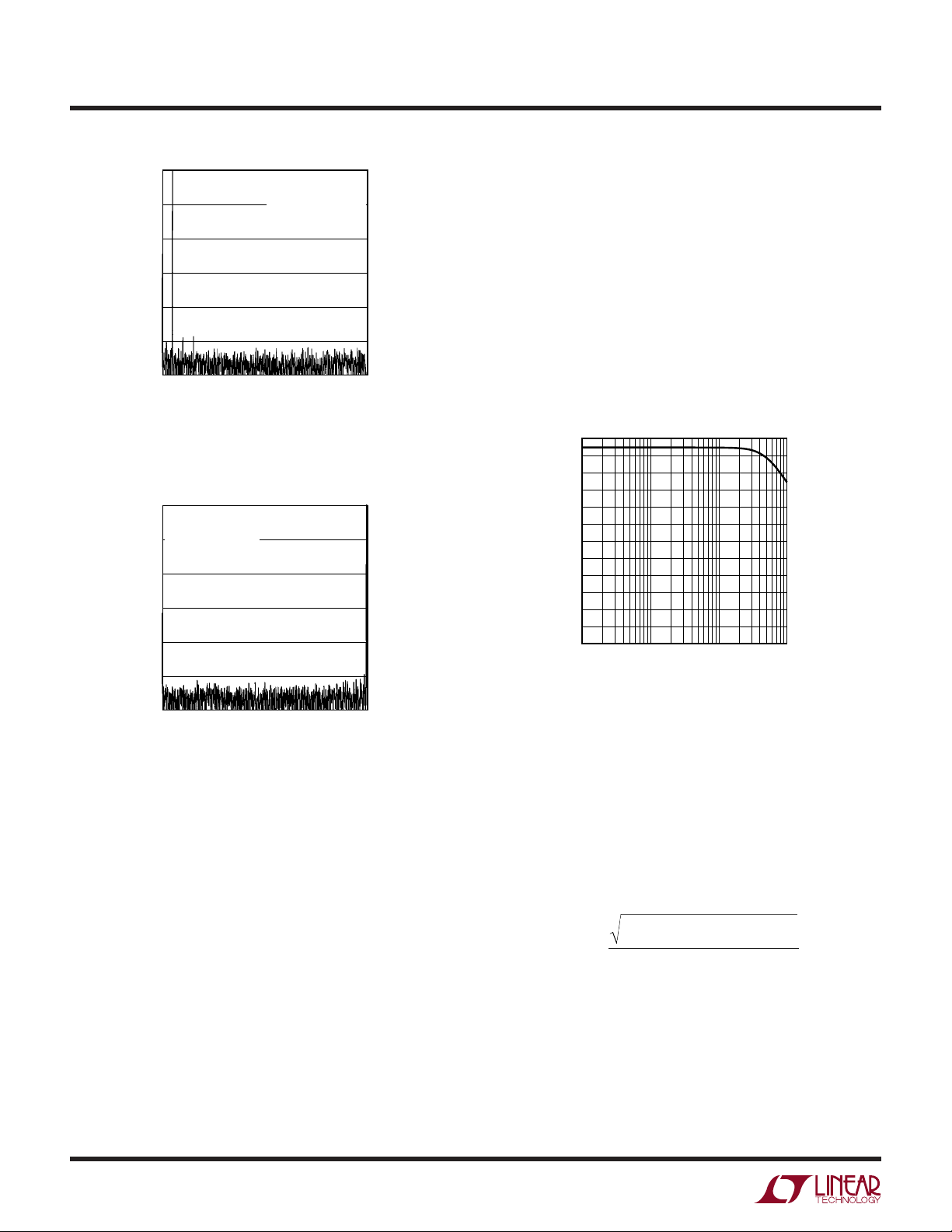
DC Performance
One way of measuring the transition noise associated with
a high resolution ADC is to use a technique where a DC
signal is applied to the input of the ADC and the resulting
output codes are collected over a large number of conversions. For example in Figure 2, the distribution of output
code is shown for a DC input that has been digitized 4096
times. The distribution is Gaussian and the RMS code
transition is about 0.33LSB.
4000
3500
3000
2500
2000
COUNTS
1500
1000
500
0
–1 0 2
–2
CODE
1
1417 F02
Figure 2. Histogram for 4096 Conversions
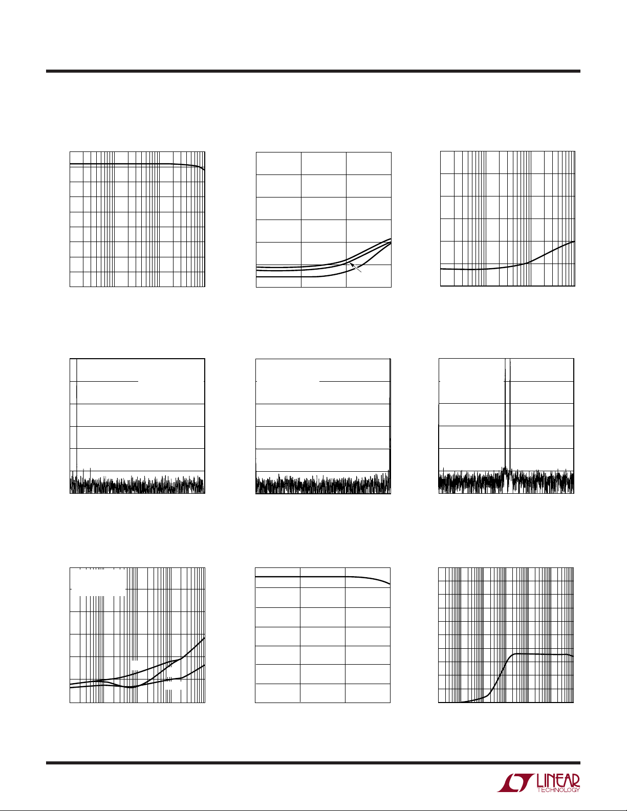
DYNAMIC PERFORMANCE
The LTC1417 has excellent high speed sampling capability. FFT (Fast Fourier Transform) test techniques are used
to test the ADC’s frequency response, distortion and
noise performance at the rated throughput. By applying
a low distortion sine wave and analyzing the digital output
using an FFT algorithm, the ADC’s spectral content can be
examined for frequencies beyond the fundamental.
Figure 3 shows a typical LTC1417 FFT plot.
9
Page 10
LTC1417
U
WUU
APPLICATIONS INFORMATION
0
–20
–40
–60
AMPLITUDE (dB)
–80
–100
–120
0 10050
Figure 3a. LTC1417 Nonaveraged, 4096 Point FFT,
Input Frequency = 10kHz
0
f
= 400kHz
SAMPLE
= 197.949188kHz
f
IN
SFDR = –98dB
–20
SINAD = 81.1dB
–40
f
SAMPLE
= 10.05859375kHz
f
IN
SFDR = –97.44dB
SINAD = 81.71dB
FREQUENCY (kHz)
= 400kHz
150
200
1417 G07
Effective Number of Bits
The effective number of bits (ENOBs) is a measurement of
the resolution of an ADC and is directly related to the
S/(N + D) by the equation:
ENOB (N) = [S/(N + D) – 1.76]/6.02
where N is the effective number of bits of resolution and
S/(N + D) is expressed in dB. At the maximum sampling
rate of 400kHz, the LTC1417 maintains near ideal ENOBs
up to the Nyquist input frequency of 200kHz (refer to
Figure 4).
14 86
80
12
10
8
EFFECTIVE BITS
6
74
68
S/(N + D) (dB)
62
–60
AMPLITUDE (dB)
–80
–100
–120
0 50 100
FREQUENCY (kHz)
150
200
1417 G08
Figure 3b. LTC1417 Nonaveraged, 4096 Point FFT,
Input Frequency = 200kHz
Signal-to-Noise Ratio
The signal-to-noise plus distortion ratio [S/(N + D)] is the
ratio between the RMS amplitude of the fundamental input
frequency to the RMS amplitude of all other frequency
components at the A/D output. The output is band limited
to frequencies from above DC and below half the sampling
frequency. Figure 3b shows a typical spectral content with
a 400kHz sampling rate and a 200kHz input. The dynamic
performance is excellent for input frequencies up to and
beyond the Nyquist limit of 200kHz.
4
2
1k
10k 100k 1M
INPUT FREQUENCY (Hz)
1417 TA02
Figure 4. Effective Bits and Signal/(Noise + Distortion)
vs Input Frequency
Total Harmonic Distortion
Total harmonic distortion (THD) is the ratio of the RMS
sum of all harmonics of the input signal to the fundamental
itself. The out-of-band harmonics alias into the frequency
band between DC and half the sampling frequency. THD is
expressed as:
222 2
VVV Vn
+++
THD Log
=
20
234
V
1
...
where V1 is the RMS amplitude of the fundamental frequency and V2 through Vn are the amplitudes of the
second through nth harmonics. THD vs Input Frequency is
shown in Figure 5. The LTC1417 has good distortion
performance up to the Nyquist frequency and beyond.
10
Page 11

LTC1417
U
WUU
APPLICATIONS INFORMATION
0
–20
–40
–60
–80
–100
AMPLITUDE (dB BELOW THE FUNDAMENTAL)
–120
1
Figure 5. Distortion vs Input Frequency
10 100
INPUT FREQUENCY (kHz)
Intermodulation Distortion
If the ADC input signal consists of more than one spectral
component, the ADC transfer function nonlinearity can
produce intermodulation distortion (IMD) in addition to
THD. IMD is the change in one sinusoidal input caused by
the presence of another sinusoidal input at a different
frequency.
If two pure sine waves of frequencies fa and fb are applied
to the ADC input, nonlinearities in the ADC transfer function can create distortion products at the sum and difference frequencies of mfa ±nfb, where m and n = 0, 1, 2, 3,
etc. For example, 2nd order IMD terms include (fa ± fb). If
the two input sine waves are equal in magnitude, the value
(in decibels) of the 2nd-order IMD products can be
expressed by the following formula:
0
f
= 400kHz
SAMPLE
= 97.303466kHz
f
IN1
= 104.632568kHz
f
–20
IN2
= 4.096V
V
IN
–40
–60
AMPLITUDE (dB)
–80
–100
–120
0
P-P
20 60 80
40 100
FREQUENCY (kHz)
THD
2ND
120
140
3RD
160 180
1417 G09
1000
1417 G05
200
Amplitude
IMD fa fb Log
+
=
()
20
at fa fb
Amplitude at fa
±
()
Peak Harmonic or Spurious Noise
The peak harmonic or spurious noise is the largest spectral component excluding the input signal and DC. This
value is expressed in decibels relative to the RMS value of
a full-scale input signal.
Full-Power and Full-Linear Bandwidth
The full-power bandwidth is the input frequency at which
the amplitude of the reconstructed fundamental is
reduced by 3dB from a full-scale input signal.
The full-linear bandwidth is the input frequency at which
the S/(N + D) has dropped to 77dB (12.5 effective bits).
The LTC1417 has been designed to optimize input bandwidth, allowing the ADC to undersample input signals with
frequencies above the converter’s Nyquist Frequency. The
noise floor stays very low at high frequencies; S/(N + D)
becomes dominated by distortion at frequencies far
beyond Nyquist.
DRIVING THE ANALOG INPUT
The differential analog inputs of the LTC1417 are easy to
drive. The inputs may be driven differentially or as a singleended input (i.e., the A
–
A
inputs are sampled at the same instant. Any
IN
–
input is grounded). The A
IN
IN
+
and
unwanted signal that is common to both inputs will be
reduced by the common mode rejection of the sampleand-hold circuit. The inputs draw only one small current
spike while charging the sample-and-hold capacitors at
the end of conversion. During conversion, the analog
inputs draw only a small leakage current. If the source
impedance of the driving circuit is low, then the LTC1417
inputs can be driven directly. As source impedance
increases, so will acquisition time (see Figure 7). For
minimum acquisition time, with high source impedance, a
buffer amplifier must be used. The only requirement is that
the amplifier driving the analog input(s) must settle after
the small current spike before the next conversion starts —
500ns for full throughput rate.
Figure 6. Intermodulation Distortion Plot
11
Page 12

LTC1417
U
WUU
APPLICATIONS INFORMATION
100
10
1
ACQUISITION TIME (µs)
0.1
0.01
Choosing an Input Amplifier
Choosing an input amplifier is easy if a few requirements
are taken into consideration. First, choose an amplifier that
has a low output impedance (<100Ω) at the closed-loop
bandwidth frequency. For example, if an amplifier is used
in a gain of 1 and has a closed-loop bandwidth of 10MHz,
then the output impedance at 10MHz must be less than
100Ω. The second requirement is that the closed-loop
bandwidth must be greater than 10MHz to ensure adequate small-signal settling for full throughput rate. If
slower op amps are used, more settling time can be
provided by increasing the time between conversions.
The best choice for an op amp to drive the LTC1417 will
depend on the application. Generally, applications fall into
two categories: AC applications where dynamic specifications are most critical and time domain applications where
DC accuracy and settling time are most critical. The
following list is a summary of the op amps that are suitable
for driving the LTC1417. More detailed information is
available in the Linear Technology Databooks and on the
LinearViewTM CD-ROM.
LT®1354: 12MHz, 400V/µs Op Amp. 1.25mA maximum
supply current. Good AC and DC specifications. Suitable
for dual supply application.
LT1357: 25MHz, 600V/µs Op Amp. 2.5mA maximum
supply current. Good AC and DC specifications. Suitable
for dual supply application.
10
1 100 1k 10k
SOURCE RESISTANCE (Ω)
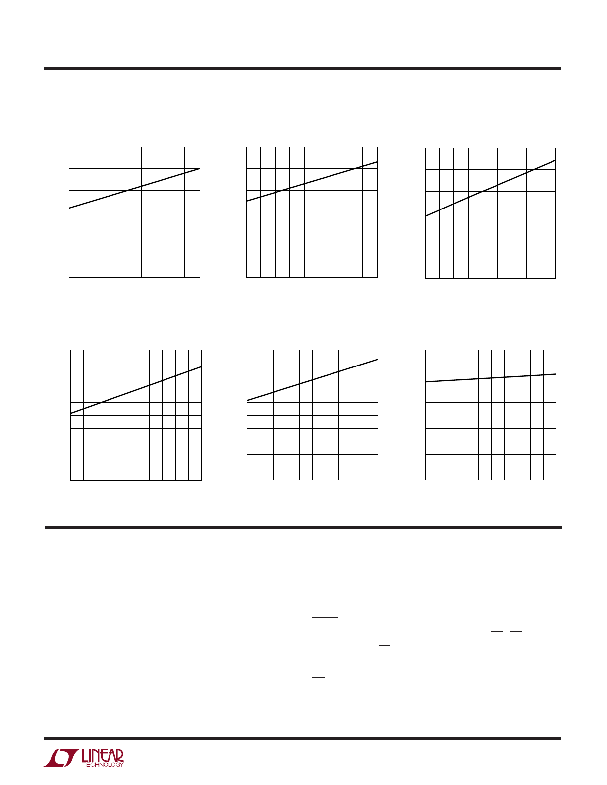
Figure 7. t
vs Source Resistance
ACQ
100k
1417 F07
LT1360: 50MHz Voltage Feedback Amplifier. 3.8mA supply current, ±2.5V to ±15V supplies. High A
VOL
, 1mV
offset and 80ns settling to 1mV (4V step, inverting and
noninverting configurations) make it suitable for fast DC
applications. Excellent AC specifications. Dual and quad
versions are available as LT1361 and LT1362.
LT1468: 90MHz Voltage Feedback Amplifier. ±5V to ±15V
supplies. Lower distortion and noise. Settles to 0.01% in
770ns. Distortion is –115dB to 20kHz.
LT1498/LT1499: 10MHz, 6V/µs, Dual/Quad Rail-to-Rail
Input and Output Op Amps. 1.7mA supply current per
amplifier. 2.2V to ±15V supplies. Good AC performance,
input noise voltage = 12nV/√Hz (typ).
LT1630/LT1631: 30MHz, 10V/µs, Dual/Quad Rail-to-Rail
Input and Output Precision Op Amps. 3.5mA supply
current per amplifier. 2.7V to ±15V supplies. Best AC
performance, input noise voltage = 6nV/√Hz (typ),
THD = –86dB at 100kHz.
LT1813: Dual 100MHz 750V/µs 3mA VFA. 5V to ±5V
supplies. Distortion is –86dB to 100kHz and – 77dB to
1MHz with ±5V supplies (2V
into 500Ω). Great part for
P-P
fast AC applications with ±5V supplies.
Input Filtering
The noise and the distortion of the input amplifier and
other circuitry must be considered since they will add to
the LTC1417 noise and distortion. The small-signal bandwidth of the sample-and-hold circuit is 10MHz. Any noise
or distortion products that are present at the analog inputs
will be summed over this entire bandwidth. Noisy input
circuitry should be filtered prior to the analog inputs to
minimize noise. A simple 1-pole RC filter is sufficient for
many applications. For example, Figure 8 shows a 1000pF
ANALOG INPUT
100Ω
1000pF
10µF
1
A
2
A
3
V
4
REFCOMP
5
AGND
IN
IN
REF
+
–
LTC1417
1417 F08
LinearView is a trademark of Linear Technology Corporation.
12
Figure 8. RC Input Filter
Page 13

LTC1417
U
WUU
APPLICATIONS INFORMATION
capacitor from + AIN to ground and a 100Ω source resistor
to limit the input bandwidth to 1.6MHz. The 1000pF
capacitor also acts as a charge reservoir for the input
sample-and-hold and isolates the ADC input from sampling glitch sensitive circuitry. High quality capacitors and
resistors should be used since these components can add
distortion. NPO and silver mica type dielectric capacitors
have excellent linearity. Carbon surface mount resistors can
also generate distortion from self heating and from damage
that may occur during soldering. Metal film surface mount
resistors are much less susceptible to both problems.
Input Range
The ±2.048V and 0V to 4.096V input ranges of the
LTC1417 are optimized for low noise and low distortion.
Most op amps also perform well over these ranges,
allowing direct coupling to the analog inputs and eliminating the need for special translation circuitry.
Some applications may require other input ranges. The
LTC1417 differential inputs and reference circuitry can
accommodate other input ranges often with little or no
additional circuitry. The following sections describe the
reference and input circuitry and how they affect the input
range.
INTERNAL REFERENCE
The LTC1417 has an on-chip, temperature compensated,
curvature corrected, bandgap reference which is factory
trimmed to 2.500V. It is internally connected to a reference
amplifier and is available at Pin 3. An 8k resistor is in series
with the output so that it can be easily overdriven in
applications where an external reference is required, see
Figure 9. A capacitor must be connected between the
5V
V
INPUT
0.1µF
1
2
3
4
5
5V
V
IN
V
LT1460-2.5
OUT
ANALOG
2.5V
10µF
Figure 9. Using the LT1460 as an External Reference
+
A
IN
–
A
IN
LTC1417
V
REF
REFCOMP
AGND
DD
1417 F09
reference amplifier compensation pin (REFCOMP, Pin 4)
and ground. The reference is stable with capacitors of 1µF
or greater. For the best noise performance, a 10µF in
parallel with a 0.1µF ceramic is recommended.
The V
pin can be driven with a DAC or other means
REF
to provide input span adjustment. The reference should
be kept in the range of 2.25V to 2.75V for specified linearity.
UNIPOLAR / BIPOLAR OPERATION AND ADJUSTMENT
Figure 10a shows the input/output characteristics for the
LTC1417. The code transitions occur midway between
successive integer LSB values (i.e., 0.5LSB, 1.5LSB,
2.5LSB, … FS – 1.5LSB). The output code is natural binary
with 1LSB = FS/16384 = 4.096V/16384 = 250µV. Figure
10b shows the input/output transfer characteristics for the
bipolar mode in two’s complement format.
FS
111...111
111...110
111...101
111...100
OUTPUT CODE
000...011
000...010
000...001
000...000
1LSB =
UNIPOLAR
ZERO
0V
LSB
1
Figure 10a. LTC1417 Unipolar Transfer Characteristics
011...111
011...110
000...001
000...000
111...111
111...110
OUTPUT CODE
100...001
100...000
Figure 10b. LTC1417 Bipolar Transfer Characteristics
4.096V
=
16384
16384
INPUT VOLTAGE (V)
BIPOLAR
ZERO
–1
LSB
INPUT VOLTAGE (V)
FS = 4.096V
1LSB = FS/16384
0V
1
LSB
FS – 1LSB
1417 F10a
FS/2 – 1LSB–FS/2
1417 F10b
13
Page 14

LTC1417
U
WUU
APPLICATIONS INFORMATION
Unipolar Offset and Full-Scale Error Adjustment
In applications where absolute accuracy is important,
offset and full-scale errors can be adjusted to zero. Offset
error must be adjusted before full-scale error. Figures
11a and 11b show the extra components required for fullscale error adjustment. Zero offset is achieved by adjusting the offset applied to the A
error, apply 125µV (i.e., 0.5LSB) at the input and adjust
the offset at the A
–
input until the output code flickers
IN
between 0000 0000 0000 00 and 0000 0000 0000 01. For
full-scale adjustment, an input voltage of 4.095625V
(FS – 1.5LSBs) is applied to A
the output code flickers between 1111 1111 1111 10 and
1111 1111 1111 11.
ANALOG INPUT
R1
OFFSET
50k
ADJ
R5
47k
10µF
R3
24k
FS
ADJ
R2
50k
–
input. For zero offset
IN
+
and R2 is adjusted until
IN
R7
R8
100Ω
R4
100Ω
R6
24k
0.1µF
48k
1
A
2
A
3
V
4
REFCOMP
5
AGND
IN
IN
REF
+
–
5V
V
DD
LTC1417
V
SS
1417 F11a
Bipolar Offset and Full-Scale Error Adjustment
Bipolar offset and full-scale errors are adjusted in a
similar fashion to the unipolar case using the circuit in
Figure 11b. Again, bipolar offset error must be adjusted
before full-scale error. Bipolar offset error adjustment is
achieved by adjusting the offset applied to the A
For zero offset error, apply – 125µV (i.e., – 0.5LSB) at A
and adjust the offset at the A
–
input until the output code
IN
IN
–
input.
IN
+
flickers between 0000 0000 0000 00 and 1111 1111 1111
11. For full-scale adjustment, an input voltage of 2.047625V
(FS – 1.5LSBs) is applied to A
+
and R2 is adjusted until
IN
the output code flickers between 0111 1111 1111 10 and
0111 1111 1111 11.
BOARD LAYOUT AND GROUNDING
To obtain the best performance from the LTC1417, a
printed circuit board with ground plane is required. The
ground plane under the ADC area should be as free of
breaks and holes as possible, such that a low impedance
path between all ADC grounds and all ADC decoupling
capacitors is provided. It is critical to prevent digital noise
from being coupled to the analog input, reference or
analog power supply lines. Layout should ensure that
digital and analog signal lines are separated as much as
possible. In particular, care should be taken not to run any
digital track alongside an analog signal track.
OFFSET
ADJ
14
Figure 11a. Offset and Full-Scale Adjust Circuit
If –5V Is Not Available
50k
–5V
R5
47k
ANALOG INPUT
R3
24k
R2
FS
50k
ADJ
R4
100Ω
R6
24k
0.1µF
R1
10µF
1
2
3
4
5
+
A
IN
–
A
IN
LTC1417
V
REF
REFCOMP
AGND
V
V
5V
DD
SS
–5V
Figure 11b. Offset and Full-Scale Adjust Circuit
If –5V Is Available
1417 F11b
An analog ground plane separate from the logic system
ground should be established under and around the ADC.
Pin 5 (AGND) and Pin 10 (DGND) and all other analog
grounds should be connected to this single analog ground
plane. The REFCOMP bypass capacitor and the VDD bypass capacitor should also be connected to this analog
ground plane. No other digital grounds should be connected to this analog ground plane. Low impedance analog and digital power supply common returns are essential
to low noise operation of the ADC and the foil width for
these tracks should be as wide as possible. In applications
where the ADC data outputs and control signals are
connected to a continuously active microprocessor bus, it
is possible to get errors in the conversion results. These
errors are due to feedthrough from the microprocessor to
the successive approximation comparator. The problem
can be eliminated by forcing the microprocessor into a
Page 15

LTC1417
U
WUU
APPLICATIONS INFORMATION
1
+
A
IN
–
A
IN
V
ANALOG
INPUT
CIRCUITRY
+
–
REF
2
3
1µF10µF
ANALOG GROUND PLANE
Figure 12. Power Supply Grounding Practice
wait state during conversion or by using three-state buffers to isolate the ADC data bus. The traces connecting the
pins and bypass capacitors must be kept short and should
be made as wide as possible.
The LTC1417 has differential inputs to minimize noise
coupling. Common mode noise on the A
will be rejected by the input CMRR. The A
used as a ground sense for the A
+
input; the LTC1417 will
IN
+
and A
IN
–
input can be
IN
IN
hold and convert the difference voltage between A
–
A
. The leads to A
IN
+
(Pin 1) and A
IN
–
(Pin 2) should be
IN
kept as short as possible. In applications where this is not
possible, the A
IN
+
and A
–
traces should be run side by
IN
side to equalize coupling.
SUPPLY BYPASSING
High quality, low series resistance ceramic, 10µF bypass
capacitors should be used at the VDD and REFCOMP pins.
Surface mount ceramic capacitors such as Taiyo Yuden
LMK325BJ106MN provide excellent bypassing in a small
board space. Alternatively 10µF tantalum capacitors in
parallel with 0.1µF ceramic capacitors can be used.
Bypass capacitors must be located as close to the pins as
possible. The traces connecting the pins and the bypass
capacitors must be kept short and should be made as wide
as possible.
10µF
–
leads
+
IN
LTC1417
AGNDREFCOMP V
54
and
DIGITAL
SS
V
15 16 10
DGND
DD
10µF
1417 F12
SYSTEM
Example Layout
Figures 13a, 13b, 13c and 13d show the schematic and
layout of a suggested evaluation board. The layout demonstrates the proper use of decoupling capacitors and ground
plane with a 2-layer printed circuit board.
POWER SHUTDOWN
The LTC1417 provides two power shutdown modes, Nap
and Sleep, to save power during inactive periods. The
Nap mode reduces ADC power dissipation by 80% and
leaves only the digital logic and reference powered up.
The wake-up time from Nap to active is 500ns (see Figure
14). In Sleep mode, all bias currents are shut down and
only leakage current remains—about 2µA. Wake-up
time from Sleep mode is much slower since the reference
circuit must power up and settle to 0.005% for full 14-bit
accuracy. Sleep mode wake-up time is dependent on the
value of the capacitor connected to the REFCOMP (Pin 4).
The wake-up time is 30ms with the recommended 10µF
capacitor. Shutdown is controlled by Pin 11 (SHDN); the
ADC is in shutdown when it is low. The shutdown mode
is selected with Pin␣ 12 (RD); low selects Nap mode, high
selects Sleep mode.
SHDN
t
1
CONVST
1417 F14
Figure 14. SHDN to CONVST Wake-Up Timing
15
Page 16

LTC1417
U
WUU
APPLICATIONS INFORMATION
C1
0.1µF
7
3
5
+
U3
LT1363CN8
2
–
8
4
C4
0.1µF
LTC1417CGN
IN
IN
REF
U1
OPTIONAL
V
DD
V
SS
BUSY
CONVST
RD
SHDN
DGND
D
OUT
BNC
BNC
JP1
R3
JP3
1µF
75Ω
C3
1000pF
50V
R4
75Ω
+
C7
C6
10µF
16V
1
2
3
4
5
6
7
8
JP5A
JP5B
JP5C
+A
–A
V
REFCOMP
AGND
EXTCLKIN
SCK
CLKOUT
R1
10k
R2
10k
JP2
J1
J2
C2
3
+
LT1363CS8
2
–
5A
0.1µF
7
5
U4
1
8
4
C5
0.1µF
5A –5A
R5
100k
JP6
JP4
C8
10µF
16V
+
5A
C9
10µF
16V
+
4
6
8
0.1µF
C12
5A
66
1
–5A
16
15
14
13
12
11
10
9
1
19
1
19
1
19
JP7
U2C
16
U2E
14
U2G
12
U2A
TC74HCT244AF
1
18
2
19
U2B
1
17
3
19
U2D
1
15
5
19
U2F
1
13
7
19
U2H
1
11
9
19
GND
–5V
E1
5V
E2
E3
+
C10
10µF
16V
AGND DGND
+
C11
10µF
16V
5A
R8
R6
100k
100k
R7
100k
5A
–5A
J3
BNC
BUSY
D
OUT
SCLK
CLKOUT
EXTCLKIN
J8
CON7
1
RD
2
3
4
5
6
7
1417 F13a
Figure 13a. Suggested Evaluation Circuit Schematic
Figure 13b. Suggested Evaluation
Circuit Board—Component Side Silkscreen
BYPASS CAPACITOR FOR U2
Figure 13c. Suggested Evaluation
Circuit Board—Component Side
Figure 13d. Suggested Evaluation
Circuit Board—Solder Side
16
Page 17

LTC1417
U
WUU
APPLICATIONS INFORMATION
DIGITAL INTERFACE
The LTC1417 operates in serial mode. The RD control input
is common to all peripheral memory interfacing. Only four
digital interface lines are required, SCLK, CONVST,
EXTCLKIN and D
be an external input or supplied by the LTC1417’s internal
clock.
Internal Clock
The ADC has an internal clock. Either the internal clock or
an external clock may be used as the conversion clock (see
Figure 15). The internal clock is factory trimmed to achieve
a typical conversion time of 1.8µs, and a maximum con-
version time over the full operating temperature range of
2.5µs. No external adjustments are required, and with the
guaranteed maximum acquisition time of 0.5µs, through-
put performance of 400ksps is assured.
Conversion Control
. SCLK, the serial data shift clock can
OUT
status is indicated by the BUSY output. BUSY is low during
a conversion.
Data Output
Output will be active when RD is low. A high RD will threestate the ouput. In unipolar mode (VSS = 0V), the data will
be in straight binary format (corresponding to the unipolar
input range). In bipolar mode (VSS = –5V), the data will be
in two’s complement format (corresponding to the bipolar
input range).
Serial Output Mode
Conversions are started by a falling CONVST edge. After a
conversion is completed and the output shift register has
been updated, BUSY will go high and valid data will be
available on D
(Pin 9). This data can be clocked out
OUT
either before the next conversion starts or it can be clocked
out during the next conversion. To enable the serial data
output buffer and shift clock, RD must be low.
Conversion start is controlled by the signal applied to the
CONVST input. A falling edge on the signal applied to the
CONVST pin starts a conversion. Once initiated, it cannot
be restarted until the conversion is complete. Converter
DATA
SAR
CLOCK
INPUT
IN
14
16 CONVERSION CLOCK CYCLES
EOC
SHIFT
REGISTER
DATA
OUT
THREE
STATE
BUFFER
DETECTOR
INTERNAL
Figure 15 shows a function block diagram of the LTC1417.
There are two pieces to this circuitry: the conversion clock
selection circuit (EXTCLKIN and CLKOUT) and the serial
port (SCLK, D
THREE
STATE
BUFFER
CLOCK
CLOCK
and RD).
OUT
• • •
• • •
7
12
9
8
6
14
SCLK
RD
D
OUT
CLKOUT
EXTCLKIN
BUSY
1417 F15
Figure 15. Functional Block Diagram
17
Page 18

LTC1417
U
WUU
APPLICATIONS INFORMATION
Conversion Clock Selection
In Figure 15, the conversion clock controls the internal
ADC operation. The conversion clock can be either internal or external. By connecting EXTCLKIN high, the internal clock is selected. This clock generates 16 clock cycles
which feed into the SAR for each conversion.
To select an external conversion clock, apply an external
conversion clock to EXTCLKIN (Pin 6). (When an external
shift clock (SCLK) is used during a conversion, the SCLK
should be used as the external conversion clock to avoid
the noise generated by the asynchronous clocks. To
maintain accuracy, the external conversion clock frequency must be between 50kHz and 9MHz.) The SAR
sends an end of conversion signal, EOC, that gates the
external conversion clock so that only 16 clock cycles can
go into the SAR, even if the external clock, EXTCLKIN,
contains more than 16 cycles.
When RD is low, these 16 cycles of conversion clock
(whether internally or externally generated) will appear
on CLKOUT during each conversion and then CLKOUT
will remain low until the next conversion. If desired,
CLKOUT can be used as a master clock to drive the serial
port. Because CLKOUT is running during the conversion,
it is important to avoid excessive loading that can cause
large supply transients and create noise. For the best
performance, limit CLKOUT loading to 20pF.
Serial Port
The serial port in Figure 15 is made up of a 16-bit shift
register and a three-state output buffer that are controlled by two inputs: SCLK and RD. The serial port has
one output, D
, that provides the serial output data.
OUT
The SCLK is used to clock the shift register. Data may be
clocked out with the internal conversion clock operating
as a master by connecting CLKOUT (Pin 8) to SCLK
(Pin␣ 7) or with an external data clock applied to SCLK.
The minimum number of SCLK cycles required to transfer a data word is 14. Normally, SCLK contains 16 clock
cycles for a word length of 16 bits; 14 bits with MSB first,
followed by two trailing zeros.
A logic high on RD disables SCLK and three-states D
OUT
.
In case of using a continuous SCLK, RD can be controlled
to limit the number of shift clocks to the desired number
(i.e., 16 cycles) and to three-state D
after the data
OUT
transfer.
In power shutdown mode (SHDN = low), a high RD
selects Sleep mode while a low RD selects Nap mode.
D
outputs the serial data; 14 bits, MSB first, on the
OUT
falling edge of each SCLK (see Figures 16 and 17). If 16
SCLKs are provided, the 14 data bits will be followed by
two zeros. The MSB (D13) will be valid on the first rising
and the first falling edge of the SCLK. D12 will be valid on
the second rising and the second falling edge as will all
the remaining bits. The data may be captured using either
edge. The largest hold time margin is achieved if data is
captured on the rising edge of SCLK.
BUSY gives the end-of-conversion indication. When the
LTC1417 is configured as a serial bus master, BUSY can
be used as a framing pulse. To three-state the serial port
after transferring the serial output data, BUSY and RD
should be connected together at the ADC (see Figure 17).
Figures 17 to 20 show several serial modes of operation,
demonstrating the flexibility of the LTC1417 serial interface.
18
SCLK
D
OUT
Figure 16. SCLK to D
OUT
V
IL
t
11
t
12
Delay
1417 F16
V
OH
V
OL
Page 19

LTC1417
U
WUU
APPLICATIONS INFORMATION
Serial Data Output During a Conversion
Using Internal Clock for Conversion and Data Transfer.
Figure 17 shows data from the previous conversion being
clocked out during the conversion with the LTC1417
internal clock providing both the conversion clock and the
SCLK. The internal clock has been optimized for the fastest
1413
BUSYCONVSTCONVST
RD
LTC1417
SCLK
8
CLKOUT
9
D
OUT
EXTCLKIN = 5
CONVST
BUSY (= RD)
CLKOUT (= SCLK)
(SAMPLE N)
t
3
t
2
t
7
2 3 4 5 6 7 8 9 10 11 12 13 14 15 16 1 2 3
1
conversion time; consequently, this mode can provide the
best overall speed performance. To select the internal
conversion clock, tie EXTCLKIN (Pin 6) high. The internal
clock appears on CLKOUT (Pin 8) which can be tied to
SCLK (Pin 7) to supply the SCLK.
BUSY (= RD)
12
7
CLKOUT ( = SCLK)
t
10
D
OUT
µP OR DSP
(CONFIGURED
AS SLAVE)
OR
SHIFT
REGISTER
(SAMPLE N + 1)
t
5
SAMPLE HOLDHOLD
t
4
OUT
Hi-Z
D
D13
D12 D11
D10D9D8D7D6D5D4D3D2D1D0
t
CONV
CLKOUT
(= SCLK)
D
OUT
D13
V
IL
t
11
t
12
CAPTURE ON
RISING CLOCK
CAPTURE ON
FALLING CLOCK
V
OH
D11D12
V
OL
FILL
ZEROS
Hi-Z
D13 D13 D12 D11
DATA NDATA (N – 1)
t
8
1417 F17
Figure 17. Internal Conversion Clock Selected. Data Transferred During Conversion Using
the ADC Clock Output as a Master Shift Clock (SCLK Driven from CLKOUT)
19
Page 20

LTC1417
U
WUU
APPLICATIONS INFORMATION
Using External Clock for Conversion and Data Transfer.
In Figure 18, data from the previous conversion is output
during the conversion with an external clock providing
both the conversion clock and the shift clock. To select an
external conversion clock, apply the clock to EXTCLKIN.
The same clock is also applied to SCLK to provide a data
1413
BUSYCONVSTCONVST
RD
LTC1417
EXTCLKIN
SCLK
9
D
OUT
CONVST
BUSY (= RD)
(SAMPLE N)
t
3
t
2
shift clock. To maintain conversion accuracy, the external
clock frequency must be between 50kHz and 9MHz.
Using an external clock to transfer data while an internal
clock controls the conversion process is not recommended. As both signals are asynchronous, clock noise
can corrupt the conversion result.
BUSY (= RD)
12
EXTCLKIN ( = SCLK)
6
7
D
t
10
OUT
µP OR DSP
(SAMPLE N + 1)
t
5
SAMPLE HOLDHOLD
EXTCLKIN (= SCLK)
D
OUT
t
dEXTCLKIN
Hi-Z
1
2 3 4 5 6 7 8 9 10 11 12 13 14 15 16 1 2 3
t
7
D13
D12 D11
D10 D9 D8 D7 D6 D5 D4 D3 D2 D1 D0
t
CONV
EXTCLKIN
(= SCLK)
D
OUT
t
LEXTCLKIN
V
IL
t
11
t
12
D13
t
CAPTURE ON
RISING CLOCK
HEXTCLKIN
CAPTURE ON
FALLING CLOCK
V
OH
D11D12
V
OL
FILL
ZEROS
Figure 18. External Conversion Clock Selected. Data Transferred During Conversion Using
the External Clock (External Clock Drives Both EXTCLKIN and SCLK)
t
4
Hi-Z
D13 D13 D12 D11
DATA NDATA (N – 1)
t
8
1417 F18
20
Page 21

LTC1417
U
WUU
APPLICATIONS INFORMATION
Serial Data Output After a Conversion
Using an Internal Conversion Clock and an External Data
Clock. In this mode, data is output after the end of each
conversion and before the next conversion is started
(Figure 19). The internal clock is used as the conversion
clock and an external clock is used for the SCLK. This
mode is useful in applications where the processor acts as
a serial bus master device. This mode is SPI and
1413
LTC1417
BUSYCONVST
RD
SCLK
D
OUT
12
7
9
EXTCLKIN = 5
CONVST
CONVST
t
2
t
3
MICROWIRETM compatible. It also allows operation when
the SCLK frequency is very low (less than 30kHz). To
select the internal conversion clock, tie EXTCLKIN high.
The external SCLK is applied to SCLK. RD can be used to
gate the external SCLK, such that data will clock only after
RD goes low and to three-state D
after data transfer. If
OUT
more than 16 SCLKs are provided, more zeros will be filled
in after the data word indefinitely.
MICROWIRE is a trademark of National Semiconductor Corporation.
INT
C0
µP OR DSP
SCK
MISO
t
10
t
5
BUSY
RD
SCLK
D
OUT
SAMPLE
t
9
V
IL
D13
t
LSCLK
t
11
t
12
CAPTURE ON
RISING CLOCK
(SAMPLE N)
Hi-Z
t
HOLD
CONV
t
6
12345678910111213141516
t
7
1211109876543210
D13
DATA N
SCLK
D
OUT
Figure 19. Internal Conversion Clock Selected. Data Transferred After Conversion
Using an External SCLK. BUSY↑ Indicates End of Conversion
FILL
ZEROS
t
HSCLK
CAPTURE ON
FALLING CLOCK
t
8
Hi-Z
1417 F19
V
OH
D11D12
V
OL
21
Page 22

LTC1417
U
WUU
APPLICATIONS INFORMATION
Using an External Conversion Clock and an External
Data Clock. In Figure 20, data is also output after each
conversion is completed and before the next conversion is
started. An external clock is used for the conversion clock
and either another or the same external clock is used for
the SCLK. This mode is identical to Figure 19 except that
an external clock is used for the conversion. This mode
allows the user to synchronize the A/D conversion to an
external clock either to have precise control of the internal
bit test timing or to provide a precise conversion time. As in
BUSY
RD
SCLK
D
OUT
613
14
12
7
9
t
4
EXTCLKIN
CONVST
BUSY
RD
t
dEXTCLKIN
t
3
CONVSTCONVST
EXTCLKIN
LTC1417
12345678910111213141516 1 2 34
t
2
HOLD
Figure 19, this mode works when the SCLK frequency is
very low (less than 30kHz). However, the external conversion clock must be between 30kHz and 9MHz to maintain
accuracy. If more than 16 SCLKs are provided, more zeros
will be filled in after the data word indefinitely. To select the
external conversion clock, apply an external conversion
clock to EXTCLKIN. The external SCLK is applied to SCLK.
RD can be used to gate the external SCLK such that data will
be clocked out only after RD goes low.
CLKOUT
INT
µP OR DSP
C0
SCK
MISO
t
10
t
6
t
5
SAMPLE
t
9
SCLK
D
OUT
22
12345678910111213141516
t
7
(SAMPLE N)
t
CONV
Hi-Z
1211109876543210
D13
DATA N
t
SCLK
D
OUT
V
IL
D13
LSCLK
t
11
t
12
CAPTURE ON
RISING CLOCK
Figure 20. External Conversion Clock Selected. Data Transferred After Conversion
Using an External SCLK. BUSY↑ Indicates End of Conversion
FILL
ZEROS
t
HSCLK
CAPTURE ON
FALLING CLOCK
t
8
Hi-Z
V
OH
D11D12
V
OL
1417 F20
Page 23

U
TYPICAL APPLICATIONS
LTC1417
Figure 21 shows the connections necessary for interfacing
the LTC1417 and LTC1391 8-channel signal acquisition
system to an SPI port. With the sample software routine
shown in Listing A, the SPI uses MOSI to send serial data
to the LTC1391 8-channel multiplexer, selecting one of
eight MUX channels.
While data is sent to the LTC1391, SPI uses MISO to
retrieve conversion data from the LTC1417. After the data
transfer is complete, the conversion start signal is sent to
0.1µF
IN1
IN2
IN3
IN4
IN5
IN6
IN7
IN8
1
S0
2
S1
LTC1391
3
S2
4
S3
5
S4
6
S5
7
S6
8
S7
D
OUT
D
CLK
DGND
16
+
V
15
D
14
–
V
13
NC
12
IN
11
CS
10
9
1µF
10µF
5V
NC
the LTC1417. The end of conversion is signaled by a logic
high on the BUSY output. When this occurs, data is
exchanged between the LTC1417/LTC1391 and the
controller.
The timing diagram in Figure 22 shows the relation between MUX channel selection data and the conversion
data that are simultaneously exchanged. There is a two
conversion delay between the MUX data selects a given
channel and when that channel’s data is retrieved.
5V5V
10µF
1
A
2
A
3
V
4
REFCOMP
5
AGND
6
EXTCLKIN
7
SCLK
8
CLKOUT
IN
IN
REF
+
–
LTC1417
V
V
BUSY
CONVST
RD
SHDN
DGND
D
OUT
16
DD
15
SS
14
13
12
11
10
9
PORT C, BIT 7
PORT C, BIT 0
SS
MC68HC11
MISO
CLK
MOSI
Figure 21. 0V to 4.096V, 8-Channel Data Acquisition System Configured
for Control and Data Retrieval by a 68HC11 µC. Code is Shown in Listing A
1417 F21
23
Page 24

LTC1417
U
TYPICAL APPLICATIONS
Listing A
***********************************************************************
* *
* This example program retrieves data from a previous LTC1417 *
* conversion and loads the next LTC1391 MUX channel. It stores the *
* 14-bit, right justified data in two consecutive memory locations. *
* It finishes by initiating the next conversion. *
* *
***********************************************************************
*
************************************
* 68HC11 register definitions *
************************************
*
PIOC EQU $1002 Parallel I/O control register
* “STAF,STAI,CWOM,HNDS, OIN, PLS, EGA,INVB”
PORTC EQU $1003 Port C data register
* “Bit7,Bit6,Bit5,Bit4,Bit3,Bit2,Bit1,Bit0”
DDRC EQU $1007 Port D data direction register
* “Bit7,Bit6,Bit5,Bit4,Bit3,Bit2,Bit1,Bit0”
* 1 = output, 0 = input
PORTD EQU $1008 Port D data register
* “ - , - , SS* ,CSK ;MOSI,MISO,TxD ,RxD “
DDRD EQU $1009 Port D data direction register
SPCR EQU $1028 SPI control register
* “SPIE,SPE ,DWOM,MSTR;SPOL,CPHA,SPR1,SPR0”
SPSR EQU $1029 SPI status register
* “SPIF,WCOL, - ,MODF; - , - , - , - “
SPDR EQU $102A SPI data register; Read-Buffer; Write-Shifter
*
* RAM variables to hold the LTC1417’s 14 conversion result
*
DIN1 EQU $00 This memory location holds the LTC1417’s bits 13 - 08
DIN2 EQU $01 This memory location holds the LTC1417’s bits 07 - 00
MUX EQU $02 This memory location holds the MUX address data
*
*******************************************
* Start GETDATA Routine *
*******************************************
*
INIT1 LDAA #$03 0,0,0,0,0,0,1,1
* “STAF=0,STAI=0,CWOM=0,HNDS=0, OIN=0, PLS=0, EGA=1,INVB=1”
* as after a reset, necessary of simple Port D manipulation
* “Bit7=input,- ,- ,- ,- ,- ,- ,Bit0=output”
* Bit7 used for BUSY signal input, Bit0 used for CONVST
* signal output
* -, -, SS*-Hi, SCK-Lo, MOSI-Hi, MISO-Hi, X, X
* MISO, TxD, RxD are configured as Inputs
* DDRD’s bit 5 is a 1 so that port D’s SS* pin is a general output
* and the clock rate is E/2
ORG $C000 Program start location
STAA PIOC Ensures that the PIOC register’s status is the same
LDAA #$01 0,0,0,0,0,0,0,1
STAA DDRC The direction of PortD’s bits are now set
LDAA PORTC Get contents of Port C
ORAA #%00000001 Set Bit0 high
STAA PORTC Initialize CONVST to a logic high
LDAA #$2F -,-,1,0;1,1,1,1
STAA PORTD Keeps SS* a logic high when DDRD, bit 5 is set
LDAA #$38 -,-,1,1;1,0,0,0
STAA DDRD SS* , SCK, MOSI are configured as Outputs
LDAA #$50
STAA SPCR The SPI is configured as Master, CPHA = 0, CPOL = 0
24
Page 25

U
TYPICAL APPLICATIONS
* (This assumes an E-Clock frequency of 4MHz. For higher
* E-Clock frequencies, change the above value of $50 to a
* value that ensures the SCK frequency is 2MHz or less.)
GETDATAPSHX
PSHY
PSHA
*
*****************************************
* Setup indecies *
*****************************************
*
LDX #$0 The X register is used as a pointer to the memory
* locations that hold the conversion data
LDY #$1000
*
*****************************************
* The next short loop ensures that the *
* LTC1417’s conversion is finished *
* before starting the SPI data transfer *
*****************************************
*
CONVENDLDAA PORTC Retrieve the contents of port D
ANDA #%10000000 Look at Bit7
* Bit7 = Hi; the LTC1417’s conversion is complete
* Bit7 = Lo; the LTC1417’s conversion is not
* complete
BPL CONVEND Branch to the loop’s beginning while Bit7 remains
* low
*
*************************************************************************
* This routine sends data to the LTC1417 and sets its MUX channel. The *
* very first time this routine is entered produces invalid data. Each *
* time thereafter, the data will correspond to the previous active *
* CONVST signal sent to the LTC1417. *
*************************************************************************
*
LDAA #$00 Dummy value for upper byte of 16-bit SPI transfer
BCLR PORTD,Y %00100000 This sets the SS* output bit to a logic
* low, selecting the LTC1417
STAA SPDR Transfer Accum. A contents to SPI register to initiate
* serial transfer
WAITMX1 LDAA SPSR Get SPI transfer status
BPL WAITMX1If the transfer is not finished, read status
LDAA SPDR Load accumulator A with the current byte of LTC1417 data
* that was just received
STAA DIN1 Transfer the LTC1417’s high byte (Bit13 - Bit6) to memory
LDAA MUX Retrieve MUX address
ORAA #$08 Set the MUX’s ENABLE bit
STAA SPDR Transfer Accum. A contents to SPI register to initiate
* serial transfer
WAITMX2 LDAA SPSR Get SPI transfer status
BPL WAITMX2If the transfer is not finished, read status
BSET PORTD,Y %00100000 This sets the SS* output bit to a logic
* high, de-selecting the LTC1417
LDAA SPDR Load accumulator A with the current byte of LTC1417 data
* that was just received
STAA DIN2 Transfer the LTC1417’s low byte (Bit5 - Bit0) to memory
LDD DIN1 Load the contents of DIN1 and DIN2 into the double
* accumulator D
LSRD
LSRD Two logical shifts to the right to right justify the
* 14-bit conversion results
STD DIN1 Place right justified result back in memory
LTC1417
25
Page 26

LTC1417
U
TYPICAL APPLICATIONS
*
*****************************************
* Initiate a LTC1417 conversion *
*****************************************
*
* low, initiating a conversion
* high, returning CONVST to a logic high
*
CONVST
BCLR PORTC,Y %00000001 This sets PORTC, Bit0 output to a logic
BSET PORTC,Y %00000001 This resets PORTC, Bit0 output to a logic
PULA Restore the A register
PULY Restore the Y register
PULX Restore the X register
RTS
BUSY
RD
MUX
DATA
ADC
DATA
MUX
OUT
CH0 CH1 CH2 CH3 CH4
CH5CH4CH3CH2CH1
CH3CH2CH1CH0CH7
1417 F22
Figure 22. This Diagram Shows the Relationship Between the Selected LTC1391 MUX Channel and the Conversion Data Retrieved
from the LTC1417 When Using the Sample Program in Listing A. At Any Point in Time, a Two Conversion Delay Exists Between the
Selected MUX Channel and When Its Data Is Retrieved
26
Page 27

U
TYPICAL APPLICATIONS
LTC1417
Figure 23 uses the DG408 to select one of eight ±2.048V
bipolar signals and apply it to the LTC1417’s analog input.
The circuit is designed to connect to a 68HC11 µC. The
MUX’s parallel input is connected to the controller’s port
C and the LTC1417’s serial interface is accessed through
the controller’s SPI interface.
0.1µF
13
+
V
3
–
V
14
2
EN
A2
A1
A0
D
0.1µF
1µF
10µF
IN1
IN2
IN3
IN4
IN5
IN6
IN7
IN8
1
S1
2
S2
3
4
5
6
7
8
DG408
S3
S4
S5
S6
S7
S8
GND
The sequence to generate a conversion is shown in sample
program Listing B. The first step selects a MUX channel.
This is followed by initiating a conversion and waiting for
BUSY to go high, signifying end of conversion. Once BUSY
goes low, the SPI is used to retrieve the 14-bit conversion
data. The timing relationships between the various control
signals and data transmission are shown in Figure 24.
5V – 5V5V –5V
V
V
BUSY
RD
SHDN
DGND
D
OUT
16
DD
15
SS
14
13
12
11
10
9
PORT C, BIT 7
PORT C, BIT 6
SS
MISO
MC68HC11
CLK
PORT C, BIT 2
PORT C, BIT 1
PORT C, BIT 0
1417 F23
5V
NC
1
A
2
A
3
V
4
REFCOMP
5
AGND
6
EXTCLKIN
7
SCLK
8
CLKOUT
IN
IN
REF
+
–
LTC1417
CONVST
Figure 23. With an Input Range of ±2.048V for Each of Eight Inputs,
This Data Acquisition System is Configured for Communication with the 68HC11 µC
27
Page 28

LTC1417
U
TYPICAL APPLICATIONS
Listing B
*************************************************************************
* *
* This example program selects a DG408 MUX channel using parallel *
* port C, initiates a conversion, and retrieves data from the LTC1417. *
* It stores the 14-bit, right justified data in two consecutive memory *
* locations. *
* *
*************************************************************************
*
*****************************************
* 68HC11 register definitions *
*****************************************
*
PIOC EQU $1002 Parallel I/O control register
* “STAF,STAI,CWOM,HNDS, OIN, PLS, EGA,INVB”
PORTC EQU $1003 Port C data register
* “Bit7,Bit6,Bit5,Bit4,Bit3,Bit2,Bit1,Bit0”
DDRC EQU $1007 Port D data direction register
* “Bit7,Bit6,Bit5,Bit4,Bit3,Bit2,Bit1,Bit0”
* 1 = output, 0 = input
PORTD EQU $1008 Port D data register
* “ - , - , SS* ,CSK ;MOSI,MISO,TxD ,RxD “
DDRD EQU $1009 Port D data direction register
SPCR EQU $1028 SPI control register
* “SPIE,SPE ,DWOM,MSTR;SPOL,CPHA,SPR1,SPR0”
SPSR EQU $1029 SPI status register
* “SPIF,WCOL, - ,MODF; - , - , - , - “
SPDR EQU $102A SPI data register; Read-Buffer; Write-Shifter
*
* RAM variables to hold the LTC1417’s 14 conversion result
*
DIN1 EQU $00 This memory location holds the LTC1417’s bits 13 - 08
DIN2 EQU $01 This memory location holds the LTC1417’s bits 07 - 00
MUX EQU $02 This memory location holds the MUX address data
*
*****************************************
* Start GETDATA Routine *
*****************************************
*
INIT1 LDAA #$03 0,0,0,0,0,0,1,1
* “STAF=0,STAI=0,CWOM=0,HNDS=0, OIN=0, PLS=0, EGA=1,INVB=1”
* as after a reset, necessary of simple Port D manipulation
* “Bit7=input,Bit6=output,- ,- ,- ,Bit2=output,Bit1=output,
* Bit0=output”
* Bit7 used for BUSY input
* Bit6 used for CONVST signal output
* Bits 2 - 0 are used for the MUX address
* -, -, SS*-Hi, SCK-Lo, MOSI-Hi, MISO-Hi, X, X
* MISO, TxD, RxD are configured as Inputs
* DDRD’s Bit5 is a 1 so that port D’s SS* pin is a general output
* and the clock rate is E/2
* (This assumes an E-Clock frequency of 4MHz. For higher
ORG $C000 Program start location
STAA PIOC Ensures that the PIOC register’s status is the same
LDAA #$47 0,1,0,0,0,1,1,1
STAA DDRC Direction of PortD’s bit are now set
LDAA #$2F -,-,1,0;1,1,1,1
STAA PORTD Keeps SS* a logic high when DDRD, Bit5 is set
LDAA #$38 -,-,1,1;1,0,0,0
STAA DDRD SS* , SCK, MOSI are configured as Outputs
LDAA #$50
STAA SPCR The SPI is configured as Master, CPHA = 0, CPOL = 0
28
Page 29

U
TYPICAL APPLICATIONS
* E-Clock frequencies, change the above value of $50 to a
* value that ensures the SCK frequency is 2MHz or less.)
GETDATAPSHX
PSHY
PSHA
*
*****************************************
* Setup indecies *
*****************************************
*
LDX #$0 The X register is used as a pointer to the memory
* locations that hold the conversion data
LDY #$1000
*
*****************************************
* Initialize the LTC1417’s CONVST input *
* to a logic high before a conversion *
* start *
*****************************************
*
BSET PORTC,Y %01000000 This sets PORTC, Bit6 output to a logic
* high, forcing CONVST to a logic high
*
*****************************************
* Retrieve the MUX address from memory *
* and send it to the DG408 *
*****************************************
*
LDAA PORTC Capture the contents of PortC
ORAA MUX “Add” the MUX address
STAA PORTC Select the MUX channel
*
*****************************************
* Initiate a LTC1417 conversion *
*****************************************
*
BCLR PORTC,Y %01000000 This sets PORTC, Bit6 output to a logic
* low, initiating a conversion
BSET PORTC,Y %01000000 This resets PORTC, Bit6 output to a logic
* high, returning CONVST to a logic high
*
*****************************************
* The next short loop ensures that the *
* LTC1417’s conversion is finished *
* before starting the SPI data transfer *
*****************************************
*
CONVENDLDAA PORTC Retrieve the contents of port D
ANDA #%10000000 Look at Bit7
* Bit7 = Hi; the LTC1417’s conversion is complete
* Bit7 = Lo; the LTC1417’s conversion is not
* complete
BPL CONVEND Branch to the loop’s beginning while Bit7
* remains high
*
*************************************************************************
* This routine sends data to the LTC1417 and sets its MUX channel. The *
* very first time this routine is entered produces invalid data. Each *
* time thereafter, the data will correspond to the previous active *
* CONVST signal sent to the LTC1417. *
*************************************************************************
*
LTC1417
29
Page 30

LTC1417
U
TYPICAL APPLICATIONS
* low, selecting the LTC1417
TRFLP1 LDAA #$0 Load accumulator A with a null byte for SPI transfer
* starts the transfer
WAIT1 LDAA SPSR This loop waits for the SPI to complete a serial
* transfer/exchange by reading the SPI Status Register
* MSB and is set to one at the end of an SPI transfer. The
* branch will occur while SPIF is a zero.
* that was just received
* the next byte for transfer/exchage
* high, de-selecting the LTC1417
* accumulator D
* conversion results
BCLR PORTD,Y %00100000 This sets the SS* output bit to a logic
STAA SPDR This writes the byte into the SPI data register and
BPL WAIT1 The SPIF (SPI transfer complete flag) bit is the SPSR’s
LDAA SPDR Load accumulator A with the current byte of LTC1417 data
STAA 0,X Transfer the LTC1417’s data to memory
INX Increment the pointer
CPX #DIN2+1Has the last byte been transferred/exchanged?
BNE TRFLP1 If the last byte has not been reached, then proceed to
BSET PORTD,Y %00100000 This sets the SS* output bit to a logic
LDD DIN1 Load the contents of DIN1 and DIN2 into the double
LSRD
LSRD Two logical shifts to right justify the 14-bit
STD DIN1 Return right justified data to memory
PULA Restore the A register
PULY Restore the Y register
PULX Restore the X register
RTS
CONVST
BUSY
RD
SCLK
D
OUT
MUX
DATA
CH0 CH1 CH2 CH3
Figure 24. Using the Sample Program In Listing 2, the LTC1417, Combined with the DG408 8-Channel MUX,
Has No Latency Between the Selected Input Voltage and Its Conversion Data as Shown In the Timing Relationship Above
CH5
CH3 DATACH2 DATACH1 DATACH0 DATA
1417 F24
30
Page 31

PACKAGEDESCRIPTI
O
U
Dimensions in inches (millimeters) unless otherwise noted.
GN Package
16-Lead Plastic SSOP (Narrow 0.150)
(LTC DWG # 05-08-1641)
0.189 – 0.196*
(4.801 – 4.978)
16
15
14
12 11 10
13
9
LTC1417
0.009
(0.229)
REF
0.015
± 0.004
(0.38 ± 0.10)
0.007 – 0.0098
(0.178 – 0.249)
0.016 – 0.050
(0.406 – 1.270)
* DIMENSION DOES NOT INCLUDE MOLD FLASH. MOLD FLASH
SHALL NOT EXCEED 0.006" (0.152mm) PER SIDE
** DIMENSION DOES NOT INCLUDE INTERLEAD FLASH. INTERLEAD
FLASH SHALL NOT EXCEED 0.010" (0.254mm) PER SIDE
0° – 8° TYP
× 45°
0.229 – 0.244
(5.817 – 6.198)
0.053 – 0.068
(1.351 – 1.727)
0.008 – 0.012
(0.203 – 0.305)
12
0.150 – 0.157**
(3.810 – 3.988)
5
4
3
678
0.004 – 0.0098
(0.102 – 0.249)
0.025
(0.635)
BSC
GN16 (SSOP) 0398
Information furnished by Linear Technology Corporation is believed to be accurate and reliable.
However, no responsibility is assumed for its use. Linear Technology Corporation makes no representation that the interconnection of its circuits as described herein will not infringe on existing patent rights.
31
Page 32

LTC1417
RELATED PARTS
PART NUMBER DESCRIPTION COMMENTS
ADCs
LTC1274/LTC1277 Low Power, 12-Bit, 100ksps ADCs with Parallel Output 10mW Power Dissipation, Parallel/Byte Interface
LTC1401 Serial 3V, 12-Bit, 200ksps ADC in SO-8 15mW, Internal Reference and Low Power Shutdown Mode
LTC1404 Serial 12-Bit, 600ksps ADC is SO-8 5V or ±5V, Internal Reference and Shutdown
LTC1412 12-Bit, 3Msps Sampling ADC with Parallel Output Best Dynamic Performance, SINAD = 72dB at Nyquist
LTC1415 Single 5V, 12-Bit, 1.25Msps ADC with Parallel Output 55mW Power Dissipation, 72dB SINAD
LTC1416 Low Power, 14-Bit, 400ksps ADC with Parallel Output 70mW Power Dissipation, 80.5dB SINAD
LTC1418 Low Power, 14-Bit, 200ksps ADC with Parallel and Serial I/O True 14-Bit Linearity, 81.5dB, SINAD, 15mW Dissipation
LTC1419 Low Power, 14-Bit, 800ksps ADC with Parallel Output True 14-Bit Linearity, 81.5dB SINAD, 150mW Dissipaton
LTC1604 16-Bit, 333ksps Sampling ADC with Parallel Output ±2.5V Input, 90dB SINAD, 100dB THD
LTC1605 Single 5V, 16-Bit, 100ksps ADC with Parallel Output Low Power, ±10V Inputs, Parallel/Byte Interface
DACs
LTC1595 Serial 16-Bit CMOS Mulitplying DAC in SO-8 ±1LSB Max INL/DNL, 1nV • sec Glitch, DAC8043 Upgrade
LTC1596 Serial 16-Bit CMOS Mulitplying DAC ±1LSB Max INL/DNL, DAC8143/AD7543 Upgrade
LTC1650 Serial 16-Bit ±5V Voltage Output DAC Low Noise and Low Glitch Rail-to-Rail V
LTC1655 Serial 16-Bit Voltage Output DAC Low Power, SO-8 with Internal Reference
LTC1658 Serial 14-Bit Voltage Output DAC Low Power, 8-Lead MSOP Rail-to-Rail V
Reference
LT1019-2.5 Precision Bandgap Reference 0.05% Max, 5ppm/°C Max
LT1460-2.5 Micropower 3-Termainal Bandgap Reference 0.075% Max, 10ppm/°C Max
LT1461-2.5 Ultraprecise Micropower Low Dropout Reference 0.04%, 3ppm/°C
OUT
OUT
32
Linear Technology Corporation
1630 McCarthy Blvd., Milpitas, CA 95035-7417
(408) 432-1900 ● FAX: (408) 434-0507
●
www.linear-tech.com
1417fs sn1417 LT/TP 0100 4K • PRINTED IN USA
LINEAR TECHNOLOGY CORPORATION 1999
 Loading...