

Page 1
INPUT FREQUENCY (Hz)
EFFECTIVE BITS
S/(N + D) (dB)
10k 100k 1M 10M
1414 TA02
1k
14
13
12
11
10
9
8
7
6
5
4
3
2
86
80
74
68
f
SAMPLE
= 2.2MHz
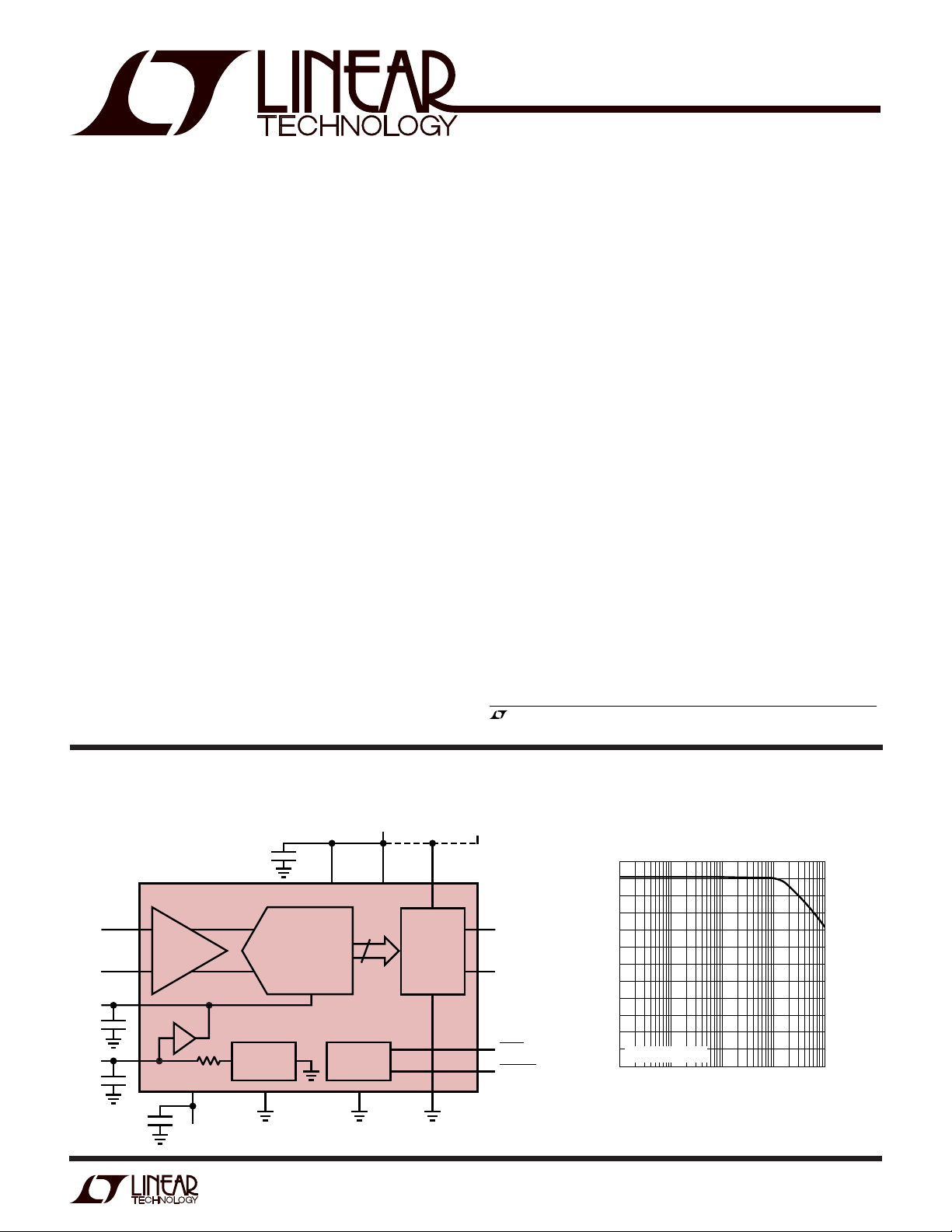
FEATURES
LTC1414
14-Bit, 2.2Msps,
Sampling A/D Converter
U
DESCRIPTIO
■
Sample Rate: 2.2Msps
■
Outstanding Spectral Purity:
80dB S/(N + D) and 95dB SFDR at 100kHz
78dB S/(N + D) and 84dB SFDR at Nyquist
■
Ultralow Distortion with Single-Ended or
Differential Inputs
■
±2.5V Bipolar Input Range Eliminates Level Shifting
and Rail-to-Rail Op Amp Requirements
■
Easy Hookup for External or Internal Reference
■
No Pipeline Delay
■
Power Dissipation: 175mW on ±5V Supplies
■
28-Pin Narrow SSOP Package
U
APPLICATIO S
■
Telecommunications
■
Digital Signal Processing
■
Multiplexed Data Acquisition Systems
■
High Speed Data Acquisition
■
Spectrum Analysis
■
Imaging Systems
The LTC®1414 is a 14-bit, 2.2Msps, sampling A/D converter which draws only 175mW from ±5V supplies. This
high performance ADC includes a high dynamic range
sample-and-hold, a precision reference and requires no
external components.
The LTC1414’s high performance sample-and-hold has a
full-scale input range of ± 2.5V. Outstanding AC performance includes 80dB S/(N + D) and 95dB SFDR with a
100kHz input. The performance remains high at the Nyquist
input frequency of 1.1MHz with 78dB S/(N + D) and 84dB
SFDR.
The unique differential input sample-and-hold can acquire
single-ended or differential input signals up to its 40MHz
bandwidth. The 70dB common mode rejection can eliminate ground loops and common mode noise by measuring
signal differentially from the source
The ADC has a microprocessor compatible, 14-bit parallel
output port. There is no pipline delay in the conversion
results.
, LTC and LT are registered trademarks of Linear Technology Corporation.
TYPICAL APPLICATIO
COMP
LTC1414
+
A
IN
S/H
–
A
IN
4.0625V
10µF
V
REF
1µF
10µF
BUFFER
–5V
2k
V
SS
14-BIT ADC
2.5V
REFERENCE
AGND
10µF
U
AV
DD
TIMING AND
LOGIC
5V
14
DGND
DV
DD
OUTPUT
BUFFERS
OPTIONAL 3V
LOGIC SUPPLY
OV
DD
•
•
•
OGND
Effective Bits and Signal-to-Noise + Distortion
vs Input Frequency
D13 (MSB)
D0 (LSB)
BUSY
CONVST
1414 TA01
1
Page 2

LTC1414
WW
W
U
ABSOLUTE MAXIMUM RATINGS
AVDD = OVDD = DVDD = V
Supply Voltage (VDD)................................................. 6V
Negative Supply Voltage (VSS) ................................–6V
Total Supply Voltage (VDD to VSS) .......................... 12V
Analog Input Voltage
(Note 3).........................(VSS – 0.3V) to (VDD + 0.3V)
Digital Input Voltage (Note 4) ..........(VSS – 0.3V) to 10V
Digital Output Voltage........(VSS – 0.3V) to (VDD + 0.3V)
Power Dissipation.............................................. 500mW
Operating Temperature Range.....................0°C to 70°C
Storage Temperature Range................. –65°C to 150°C
Lead Temperature (Soldering, 10 sec)..................300°C
(Notes 1, 2)
DD
W
PACKAGE/ORDER INFORMATION
TOP VIEW
+
1
A
IN
–
2
A
IN
3
V
REF
REFCOMP
D13 (MSB)
Consult factory for Industrial, Military and A grade parts.
4
5
AGND
6
7
D12
8
D11
9
D10
10
D9
11
D8
12
D7
13
D6
14
OGND
GN PACKAGE
28-LEAD PLASTIC SSOP
T
= 110°C, θJA = 110°C/W
JMAX
28
27
26
25
24
23
22
21
20
19
18
17
16
15
AV
DD
AGND
V
SS
BUSY
CONVST
DGND
DV
DD
OV
DD
D0
D1
D2
D3
D4
D5
ORDER PART
NUMBER
LTC1414CGN
UU
U
With internal reference (Notes 5, 6)
–
+
= A
IN
) < 2.5V 70 dB
IN
LTC1414
● ±24 LSB
RMS
U
IN
IN
VERTER
CCHARA TERIST
External Reference = 2.5V ±5 ±25 LSB
External Reference = 2.5V ±1 ppm/°C
ICS
U
PUT
LOG
Analog Input Range 4.75V ≤ VDD ≤ 5.25V, –5.25V ≤ VSS ≤ –4.75V ● ±2.5 V
Analog Input Leakage Current Between Conversions ● ±1 µA
Analog Input Capacitance Between Conversions 8 pF
Sample-and-Hold Acquisition Time ● 40 100 ns
Sample-and-Hold Aperture Delay Time –1 ns
Sample-and-Hold Aperture Delay Time Jitter 3 ps
IA
(Note 5)
During Conversions 4 pF
CO
PARAMETER CONDITIONS MIN TYP MAX UNITS
Resolution (No Missing Codes) ● 13 Bits
Integral Linearity Error (Note 7) ● ±0.75 ±2.0 LSB
Differential Linearity Error ● ±0.75 ±1.75 LSB
Offset Error (Note 8) ±5 ±20 LSB
Full-Scale Error Internal Reference ±10 ±60 LSB
Full-Scale Tempco Internal Reference ±15 ppm/°C
A
SYMBOL PARAMETER CONDITIONS MIN TYP MAX UNITS
V
I
IN
C
t
ACQ
t
AP
t
jitter
CMRR Analog Input Common Mode Rejection Ratio –2.5V < (A
2
Page 3
LTC1414
W
U
IC
DY
SYMBOL PARAMETER CONDITIONS MIN TYP MAX UNITS
S/(N + D) Signal-to-Noise Plus Distortion Ratio 100kHz Input Signal 80 dB
THD Total Harmonic Distortion 100kHz Input Signal, First 5 Harmonics –95 dB
SFDR Spurious Free Dynamic Range 100kHz Input Signal, First 5 Harmonics 95 dB
IMD Intermodulation Distortion f
A
Full Power Bandwidth 40 MHz
Full Linear Bandwidth S/(N + D) ≥ 74dB 3 MHz
ACCURAC Y
(Note 5)
1.1MHz Input Signal 78 dB
1.1MHz Input Signal, First 5 Harmonics –83 dB
1.1MHz Input Signal, First 5 Harmonics 84 dB
= 29.37kHz, f
IN1
= 32.446kHz –86 dB
IN2
U
I TER AL REFERE CE CHARACTERISTICS
PARAMETER CONDITIONS MIN TYP MAX UNITS
V
REF
V
REF
V
REF
V
REF
COMP Output Voltage I
UU
(Note 5)
Output Voltage I
Output Tempco I
Line Regulation 4.75V ≤ VDD ≤ 5.25V 0.01 LSB/V
Output Resistance I
= 0 2.480 2.500 2.520 V
OUT
= 0 ±15 ppm/°C
OUT
–5.25V ≤ V
OUT
= 0 4.06 V
OUT
≤ –4.75V 0.01 LSB/V
SS
≤ 0.1mA 2 kΩ
UU
DIGITAL I PUTS AND OUTPUTS
SYMBOL PARAMETER CONDITIONS MIN TYP MAX UNITS
V
IH
V
IL
I
IN
C
IN
V
OH
V
OL
I
SOURCE
I
SINK
High Level Input Voltage V
Low Level Input Voltage VDD = 4.75V ● 0.8 V
Digital Input Current VIN = 0V to V
Digital Input Capacitance 1.2 pF
High Level Output Voltage VDD = 4.75V, IO = –10µA 4.74 V
Low Level Output Voltage VDD = 4.75V, IO = 160µA 0.05 V
Output Source Current V
Output Sink Current V
(Note 5)
= 5.25V ● 2.4 V
DD
DD
VDD = 4.75V, IO = –200µA ● 4.0 V
VDD = 4.75V, IO = 1.6mA ● 0.10 0.4 V
= 0V –10 mA
OUT
= V
OUT
DD
● ±10 µA
10 mA
U
W
POWER REQUIRE E TS
SYMBOL PARAMETER CONDITIONS MIN TYP MAX UNITS
V
DD
V
SS
I
DD
I
SS
P
D
Positive Supply Voltage (Note 9) 4.75 5.25 V
Negative Supply Voltage (Note 9) –4.75 –5.25 V
Positive Supply Current CS High ● 12 16 mA
Negative Supply Current CS High ● 23 30 mA
Power Dissipation 175 230 mW
(Note 5)
3
Page 4
LTC1414
INPUT FREQUENCY (Hz)
10k
DISTORTION (dB)
0
–10
–20
–30
–40
–50
–60
–70
–80
–90
–100
100k 1M 10M
1414 G03
2nd
THD
3rd
W
U
TI I G CHARACTERISTICS
SYMBOL PARAMETER CONDITIONS MIN TYP MAX UNITS
f
SAMPLE(MAX)
t
CONV
t
ACQ
t
THROUGHPUT
t
1
t
2
t
3
t
4
t
5
t
6
The ● denotes specifications which apply over the full operating
temperature range; all other limits and typicals TA = 25°C.
Note 1: Absolute Maximum Ratings are those values beyond which the life
of a device may be impaired.
Note 2: All voltage values are with respect to ground with DGND and
AGND wired together (unless otherwise noted).
Note 3: When these pin voltages are taken below V
will be clamped by internal diodes. This product can handle input currents
greater than 100mA below VSS or above VDD without latchup.
Note 4: When these pin voltages are taken below V
by internal diodes. This product can handle input currents greater than
100mA below VSS without latchup. These pins are not clamped to VDD.
Note 5: V
otherwise specified.
Maximum Sampling Frequency ● 2.2 MHz
Conversion Time ● 220 330 400 ns
Acquisition Time ● 40 100 ns
Throughput Time (Acquisition + Conversion) ● 370 454 ns
CONVST to BUSY Delay CL = 25pF 10 ns
Data Ready Before BUSY↑ ±20 ns
Delay Between Conversions (Note 9) ● 100 ns
CONVST Low Time (Note 10) ● 40 ns
CONVST High Time (Note 10) ● 40 ns
Aperture Delay of Sample-and-Hold –1 ns
SS
SS
= 5V, VSS = –5V, f
DD
= 2.2MHz and tr = tf = 5ns unless
SAMPLE
(Note 5)
or above VDD, they
, they will be clamped
Note 6: Linearity, offset and full-scale specifications apply for a singleended A
+
input with A
IN
–
grounded.
IN
Note 7: Integral nonlinearity is defined as the deviation of a code from a
straight line passing through the actual endpoints of the transfer curve.
The deviation is measured from the center of the quantization band.
Note 8: Bipolar offset is the offset voltage measured from –0.5LSB
when the output code flickers between 0000 0000 0000 00 and
1111 1111 1111 11.
Note 9: Recommended operating conditions.
Note 10: The falling CONVST edge starts a conversion. If CONVST returns
high at a critical point during the conversion it can create small errors. For
best results ensure that CONVST returns high either within 225ns after the
start of the conversion or after BUSY rises.
TYPICAL PERFOR A CE CHARACTERISTICS
4
UW
Signal-to-Noise Ratio vs Input
S/(N + D) vs Input Frequency Distortion vs Input Frequency
14
13
12
11
10
9
8
7
EFFECTIVE BITS
6
5
4
3
f
= 2.2MHz
SAMPLE
2
1k
10k 100k 1M 10M
INPUT FREQUENCY (Hz)
86
80
74
68
S/(N + D) (dB)
1414 TA02
Frequency
90
80
70
60
50
40
30
20
SIGNAL-TO-NOISE RATIO (dB)
10
0
10k
100k 1M 10M
INPUT FREQUENCY (Hz)
1414 G02
Page 5

UW
OUTPUT CODE
0 4096 8192 12288 16384
DNL (LSBs)
1414 G06
2.0
1.0
0
–1.0
–2.0
TYPICAL PERFOR A CE CHARACTERISTICS
LTC1414
Spurious-Free Dynamic Range vs
Input Frequency Intermodulation Distortion Plot
0
–10
–20
–30
–40
–50
–60
–70
–80
–90
SPURIOUS-FREE DYNAMIC RANGE (dB)
–100
10k
100k 1M 10M
INPUT FREQUENCY (Hz)
Integral Nonlinearity vs Output
Code
2.0
1.0
0
INL (LSBs)
–1.0
–2.0
0 4096 8192 12288 16384
OUTPUT CODE
1414 G04
1414 G07
0
–20
–40
–60
AMPLITUDE (dB)
–80
–100
–120
0
FREQUENCY (kHz)
f
SAMPLE
f
IN1
f
IN2
400 800200 600 1000
Power Supply Feedthrough vs
Ripple Frequency
0
–20
–40
–60
–80
FEEDTHROUGH (dB)
–100
AMPLITUDE OF POWER SUPPLY
–120
0 2M4M6M8M10M
VSS (V
V
DD
OGND (V
OV
RIPPLE FREQUENCY (Hz)
= 0.02V)
RIPPLE
(V
= 0.2V)
RIPPLE
= 0.5V)
RIPPLE
(V
RIPPLE
= 0.5V)
DD
= 2.2MHz
= 80.566kHz
= 97.753kHz
1414 F05a
1414 G08
Differential Nonlinearity vs
Output Code
Input Common Mode Rejection vs
Input Frequency
80
70
60
50
40
30
20
COMMON MODE REJECTION (dB)
10
0
1k
10k 100k
INPUT FREQUENCY (Hz)
1M 10M
LTC1414 • F12
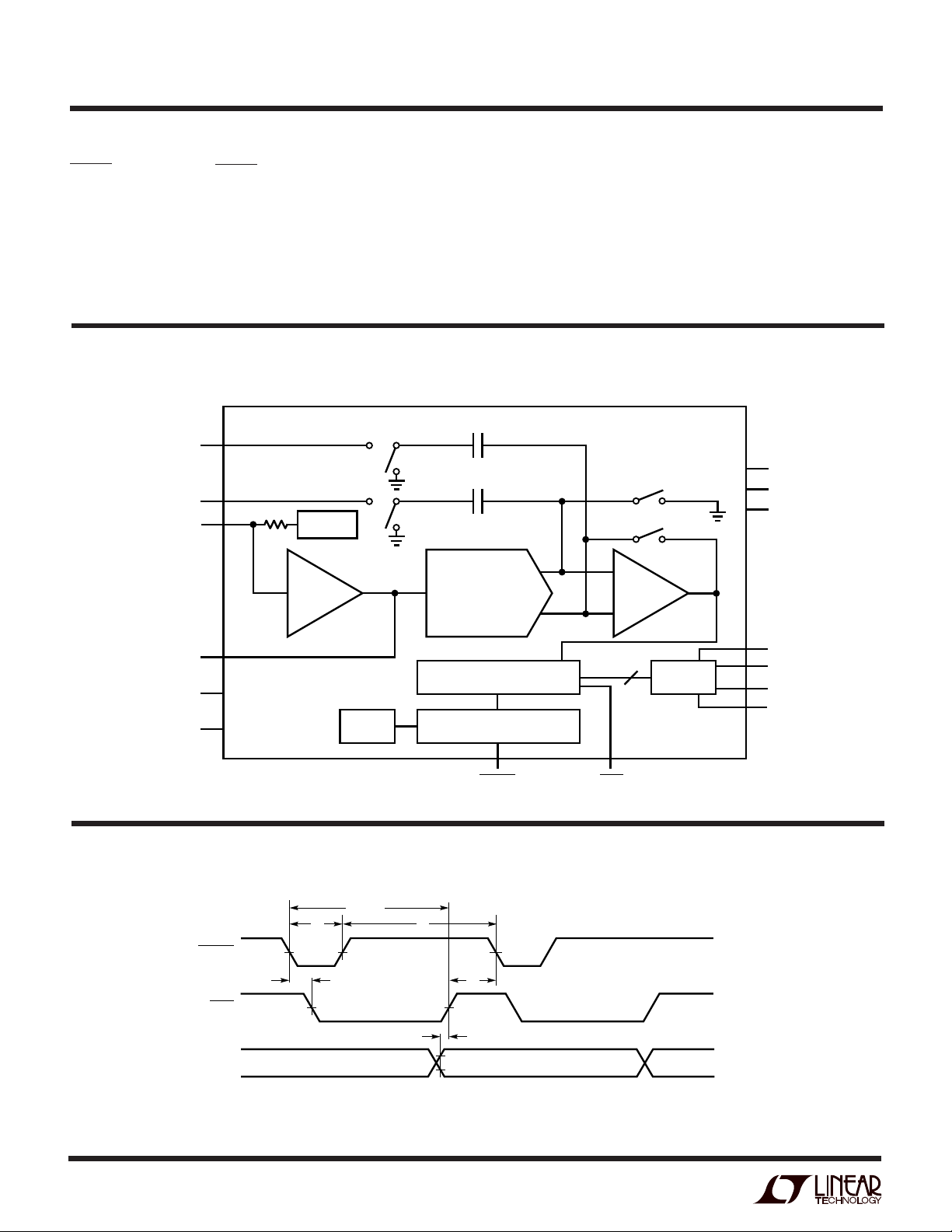
PIN FUNCTIONS
+
A
(Pin 1):
IN
when A
IN
differentially with A
–
A
(Pin 2): Negative Analog Input. Can be grounded or
IN
driven differentially with A
V
(Pin 3): 2.5V Reference Output.
REF
REFCOMP (Pin 4): 4.06V Reference Bypass Pin.
Bypass to AGND with 10µ F ceramic or 10 µF tantalum in
parallel with 0.1µF ceramic.
AGND (Pin 5): Analog Ground.
D13 to D6 (Pins 6 to 13): Data Outputs.
Positive Analog Input. ± 2.5V input range
–
is grounded. ±2.5V differential if A
IN
+
.
UUU
OGND (Pin 14): Digital Ground for the Output Drivers. Tie
to AGND
D5 to D0 (Pins 15 to 20): Data Outputs.
OVDD (Pin 21):
Positive Supply for the Output Drivers. Tie
to Pin 28 when driving 5V logic. For 3V logic, tie to supply
of the logic being driven.
DVDD (Pin 22): 5V Positive Supply. Tie to Pin 28.
DGND (Pin 23): Digital Ground. Tie to AGND.
CONVST (Pin 24): Conversion Start Signal. This active low
signal starts a conversion on its falling edge.
IN
–
is driven
IN
+
.
5
Page 6
LTC1414
PIN FUNCTIONS
UUU
BUSY (Pin 25): The BUSY Output Shows the Converter
Status. It is low when a conversion is in progress.
VSS (Pin 26): –5V Negative Supply. Bypass to AGND with
10µ F ceramic or 10µF tantalum in parallel with 0.1µF
ceramic.
UU
W
FUNCTIONAL BLOCK DIAGRA
C
+
A
IN
C
–
A
IN
V
REF
2k
2.5V REF
14-BIT CAPACITIVE DAC
AGND (Pin 27): Analog Ground.
AVDD (Pin 28): 5V Positive Supply. Bypass to AGND with
10µ F ceramic or 10µF tantalum in parallel with 0.1µF
ceramic.
SAMPLE
AV
SAMPLE
ZEROING SWITCHES
+
COMPREF AMP
–
DV
V
DD
DD
SS
REFCOMP
(4.06V)
AGND
DGND
UWW
TI I G DIAGRA
CONVST
BUSY
DATA
t
4
t
1
DATA (N – 1)
DB13 TO DB0
INTERNAL
CLOCK
t
CONV
SUCCESSIVE APPROXIMATION
REGISTER
CONTROL LOGIC
CONVST
t
5
t
3
t
2
DB13 TO DB0
DATA N
BUSY
14
OUTPUT
LATCHES
DATA (N + 1)
DB13 TO DB0
1414 BD
1414 TD
OV
DD
D13
•
•
•
D0
OGND
6
Page 7

LTC1414
U
WUU
APPLICATIONS INFORMATION
CONVERSION DETAILS
The LTC1414 uses a successive approximation algorithm
and an internal sample-and-hold circuit to convert an
analog signal to a 14-bit parallel output. The ADC is
complete with a precision reference and an internal clock.
The device is easy to interface with microprocessors and
DSPs. (Please refer to the Digital Interface section for the
data format.)
Conversion start is controlled by the CONVST input. At the
start of the conversion the successive approximation
register (SAR) is reset. Once a conversion cycle has begun
it cannot be restarted.
During the conversion, the internal differential 14-bit
capacitive DAC output is sequenced by the SAR from the
most significant bit (MSB) to the least significant bit
(LSB). Referring to Figure 1, the A
connected to the sample-and-hold capacitors (C
during the acquire phase, and the comparator offset is
nulled by the zeroing switches. In this acquire phase, a
minimum delay of 70ns will provide enough time for the
sample-and-hold capacitors to acquire the analog signal.
During the convert phase the comparator zeroing switches
open, putting the comparator into compare mode. The
input switches connect the C
SAMPLE
transferring the differential analog input charge onto the
summing junction. This input charge is successively compared with the binary-weighted charges supplied by the
differential capacitive DAC. Bit decisions are made by the
high speed comparator. At the end of a conversion, the
differential DAC output balances the A
charges. The SAR contents (a 14-bit data word) which
represents the difference of A
the 14-bit output latches.
+
and A
IN
IN
capacitors to ground,
+
and A
IN
IN
+
and A
–
are loaded into
IN
–
inputs are
SAMPLE
–
input
IN
)
+
C
HOLD
HOLD
SAMPLE
C
SAMPLE
C
DAC
–
+
ZEROING SWITCHES
HOLD
HOLD
SAMPLE
+
A
IN
SAMPLE
–
A
IN
+
–
C
DAC
+
V
DAC
–
V
DAC
SAR
–
14
COMP
OUTPUT
LATCH
D13
D0
1414 F01
Figure 1. Simplified Block Diagram
Signal-to-Noise Ratio
The signal-to-(noise + distortion) ratio [S/(N + D)] is the
ratio between the RMS amplitude of the fundamental input
frequency to the RMS amplitude of all other frequency
components at the A/D output. The output is band limited
to frequencies from above DC and below half the sampling
frequency. Figure 2a shows a typical spectral content with
a 2.2MHz sampling rate and a 100kHz input. The dynamic
performance is excellent for input frequencies up to and
beyond the Nyquist limit of 1.1MHz. (See Figure 2b)
0
–20
–40
–60
AMPLITUDE (dB)
–80
SINAD = 80dB
SFDR = 96dB
f
= 2.2MHz
SAMPLE
fIN = 97.753kHz
DYNAMIC PERFORMANCE
The LTC1414 has excellent high speed sampling capability. FFT (Fast Four Transform) test techniques are used to
test the ADC’s frequency response, distortion and noise at
the rated throughput. By applying a low distortion sine
wave and analyzing the digital output using an FFT algorithm, the ADC’s spectral content can be examined for
frequencies outside the fundamental. Figure 2 shows a
typical LTC1414 FFT plot.
–100
–120
0
400 800200 600 1000
FREQUENCY (kHz)
1414 F02a
Figure 2a. LTC1414 Nonaveraged, 2048 Point FFT,
Input Frequency = 100kHz
7
Page 8

LTC1414
U
WUU
APPLICATIONS INFORMATION
0
SINAD = 78dB
SFDR = 84dB
–20
f
= 2.2MHz
SAMPLE
fIN = 997.949kHz
–40
–60
AMPLITUDE (dB)
–80
–100
–120
0
Figure 2b. LTC1414 2048 Point FFT,
Input Frequency = 1MHz
Effective Number of Bits
The effective number of bits (ENOBs) is a measurement of
the resolution of an ADC and is directly related to the
S/(N + D) by the equation:
ENOBS = [S/(N + D) – 1.76]/6.02
where S/(N + D) is expressed in dB. At the maximum
sampling rate of 2.2MHz the LTC1414 maintains near ideal
ENOBs up to the Nyquist input frequency of 1.1MHz. Refer
to Figure 3.
Total Harmonic Distortion
400 800200 600 1000
FREQUENCY (kHz)
1414 F02b
14
13
12
11
10
9
8
7
EFFECTIVE BITS
6
5
4
3
f
SAMPLE
2
1k
= 2.2MHz
10k 100k 1M 10M
INPUT FREQUENCY (Hz)
86
80
74
68
S/(N + D) (dB)
1414 TA02
Figure 3. Effective Bits and Signal/(Noise + Distortion)
vs Input Frequency
0
–10
–20
–30
–40
–50
–60
DISTORTION (dB)
–70
–80
–90
–100
1 100k 1M 10M
2nd
10k
INPUT FREQUENCY (Hz)
THD
3rd
1414 F04
Figure 4. Distortion vs Input Frequency
Total harmonic distortion (THD) is the ratio of the RMS
sum of all harmonics of the input signal to the fundamental
itself. The out-of-band harmonics alias into the frequency
band between DC and half the sampling frequency. THD is
expressed as:
2
2
22
4
V
1
N
THD
=
20
VVV V
+++…
2
log
3
where V1 is the RMS amplitude of the fundamental frequency and V2 through VN are the amplitudes of the
second through Nth harmonics. THD vs input frequency is
shown in Figure 4. The LTC1414 has good distortion
performance up to the Nyquist frequency and beyond.
8
Intermodulation Distortion
If the ADC input signal consists of more than one spectral
component, the ADC transfer function nonlinearity can
produce intermodulation distortion (IMD) in addition to
the THD. IMD is the change in one sinusoidal input caused
by the presence of another sinusoidal input at a different
frequency.
If two pure sine waves of frequencies fa and fb are applied
to the ADC input, nonlinearities in the ADC transfer function can create distortion products at the sum and difference frequencies of mfa ± nfb, where m and n = 0, 1, 2, 3
etc. For example, the 2nd order IMD terms include (fa ± fb).
If the two input sine waves are equal in magnitude, the
value (in dB) of the 2nd order IMD products can be
expressed by the following formula:
Page 9

LTC1414
U
WUU
APPLICATIONS INFORMATION
IMD f f
±
ab
=
()
20log
0
–20
–40
–60
AMPLITUDE (dB)
–80
–100
–120
0
Figure 5a. Intermodulation Distortion Plot
with Inputs at 80kHz and 97kHz
0
–20
–40
–60
AMPLITUDE (dB)
–80
–100
–120
0
Figure 5b. Intermodulation Distortion Plot
with Input Signals of 1MHz and 1.5MHz
400 800200 600 1000
FREQUENCY (kHz)
400 800200 600 1000
FREQUENCY (kHz)
amplitudeat f f
amplitudeat f
f
= 2.2MHz
SAMPLE
f
= 80.566kHz
IN1
f
= 97.753kHz
IN2
f
= 2.2MHz
SAMPLE
f
= 970.019kHz
IN1
f
= 1.492MHz
IN2
±
()
ab
a
1414 F05a
1414 F05b
The full-linear bandwidth is the input frequency at which
the S/(N + D) has dropped to 74dB (12 effective bits). The
LTC1414 has been designed to optimize input bandwidth,
allowing the ADC to undersample input signals with frequencies above the converter’s Nyquist frequency. The
noise floor stays very low at high frequencies; S/(N + D)
becomes dominated by distortion at frequencies far beyond Nyquist.
Driving the Analog Input
The differential analog inputs of the LTC1414 are easy to
drive. The inputs may be driven differentially or as a singleended input (i.e., the
–
A
inputs are sampled at the same instant. Any
IN
–
A
input is grounded). The A
IN
IN
+
and
unwanted signal that is common mode to both inputs will
be reduced by the common mode rejection of the sampleand-hold circuit. The inputs draw only one small current
spike while charging the sample-and-hold capacitors at
the end of conversion. During conversion, the analog
inputs draw only a small leakage current. If the source
impedance of the driving circuit is low then the LTC1414
inputs can be driven directly. As source impedance
increases so will acquisition time (see Figure 6). For
minimum acquisition time, with high source impedance, a
buffer amplifier should be used. The only requirement is
that the amplifier driving the analog input(s) must settle
after the small current spike before the next conversion
starts (settling time must be 70ns for full throughput rate).
10
1
Peak Harmonic or Spurious Noise
The peak harmonic or spurious noise is the largest spectral component excluding the input signal and DC. This
value is expressed in dB relative to the RMS value of a fullscale input signal.
Full-Power and Full-Linear Bandwidth
The full-power bandwidth is that input frequency at which
the amplitude of the reconstructed fundamental is reduced by 3db for a full-scale input signal.
0.1
ACQUISITION TIME (µs)
0.01
10
Figure 6. Acquisition Time vs Source Resistance
100 1k
SOURCE RESISTANCE (Ω)
10k 100k
1414 FO6
9
Page 10

LTC1414
U
WUU
APPLICATIONS INFORMATION
Choosing an Input Amplifier
Choosing an input amplifier is easy if a few requirements
are taken into consideration. First, to limit the magnitude
of the voltage spike seen by the amplifier from charging
the sampling capacitor, choose an amplifier that has a low
output impedance (<100Ω) at the closed-loop bandwidth
frequency. For example, if an amplifier is used in a gain of
1 and has a unity-gain bandwidth of 50MHz, then the
output impedance at 50MHz must be less than 100Ω. The
second requirement is that the closed-loop bandwidth
must be greater than 40MHz to ensure adequate smallsignal settling for full throughput rate. If slower op amps
are used, more settling time can be provided by increasing
the time between conversions.
The best choice for an op amp to drive the LTC1414 will
depend on the application. Generally applications fall into
two categories: AC applications where dynamic specifications are most critical and time domain applications where
DC accuracy and settling time are most critical. The
following list is a summary of the op amps that are suitable
for driving the LTC1414. More detailed information is
available in the Linear Technology Databooks and on the
LinearViewTM CD-ROM.
AC Coupled Inputs
In applications where only the AC component of the analog
input is important, it may be desirable to AC couple the
input. This is easily accomplished by DC biasing the
LTC1414 analog input with a resistor to ground and using
a coupling capacitor to the input. Figure 7 shows a simple
AC coupled input circuit for the LTC1414 using only two
additional components. C1 is a 10µF ceramic capacitor
and R1 is a 1000Ω resistor to ground. R1 and C1 form a
highpass filter with a lower cut off frequency of 1/2π(C1)R1
or 15.9Hz.
C1
ANALOG INPUT
10µF
R1
1k
Figure 7. AC Coupled Input
1µF
10µF
1
2
3
4
5
+
A
IN
–
A
IN
LTC1414
V
REF
REFCOMP
AGND
LTC1414 • F07
LT®1223: 100MHz Video Current Feedback Amplifier.
6mA supply current. ± 5V to ± 15V supplies. Low noise.
Good for AC applications.
LT1227: 140MHz Video Current Feedback Amplifier. 10mA
supply current. ±5V to ±15V supplies. Low noise. Best for
AC applications.
LT1229/LT1230: Dual and Quad 100MHz Current Feedback Amplifiers. ±2V to ±15V supplies. Low noise. Good
AC specifications, 6mA supply current each amplifier.
LT1360: 50MHz Voltage Feedback Amplifier. 3.8mA supply current. Good AC and DC specs. ±5V to ±15V supplies.
70ns settling to 0.5LSB.
LT1363: 70MHz, 1000V/µs Op Amps. 6.3mA supply cur-
rent. Good AC and DC specifications. 60ns settling to
0.5LSB.
LT1364/LT1365: Dual and Quad 70MHz, 1000V/µs Op
Amps. 6.3mA supply current per amplifier. 60ns settling
to 0.5LSB.
LinearView is a trademark of Linear Technology Corporation.
Differential Drive
In some applications the ADC drive circuitry is differential.
The differential drive can be applied directly to the LTC1414
without any special translation circuitry. Differential drive
can be advantageous at high frequencies (>1MHz) since it
provides improved THD and SFDR. Transformers can be
used to provide AC coupling, input scaling and single
ended to differential conversion as shown in Figure 8. The
resistor RS across the secondary will determine the input
impedance on the primary. The input impedance of the
primary RP will be related to the secondary load resistor R
S
by the equation
RP = RS/n
2
For example, if a Minicircuits T4-6T transformer is used,
the turns ratio is 2; if RS is 200Ω then RP is equal to 50Ω.
The center tap of the secondary will set the common
mode voltage and should be grounded for optimal AC
performance.
10
Page 11

LTC1414
U
WUU
APPLICATIONS INFORMATION
R1
100Ω
50Ω
R
S
R2
50Ω
500pF
10µF
1
2
3
4
5
C1
500pF
1µF
10µF
+
A
IN
–
A
IN
LTC1414
V
REF
REFCOMP
AGND
1
2
3
4
5
+
A
IN
–
A
IN
LTC1414
V
REF
REFCOMP
AGND
LTC1414 • F09
LTC1414 • F08
+
A
IN
1:N
P
ANALOG
INPUT
R
Figure 8. If a Transformer Coupled Input is Required,
this Circuit Provides a Simple Solution
Input Filtering
The noise and the distortion of the input amplifier and
other circuitry must be considered since they will add to
the LTC1414 noise and distortion. The small-signal bandwidth of the sample-and-hold circuit is 40MHz. Any noise
or distortion products that are present at the analog inputs
will be summed over this entire bandwidth. Noisy input
circuitry should be filtered prior to the analog inputs to
minimize noise. A simple 1-pole RC filter is sufficient for
many applications.
For example, Figure 9 shows a 500pF capacitor from
to ground and a 100Ω source resistor to limit the input
bandwidth to 3.2MHz. The 500pF capacitor also acts as a
charge reservoir for the input sample-and-hold and isolates the ADC input from sampling glitch-sensitive circuitry. High quality capacitors and resistors should be
used since poor quality components can add distortion.
NPO and silver mica type dielectric capacitors have excellent linearity. Carbon surface mount resistors can also
generate distortion from self heating and from damage
that may occur during soldering. Metal film surface mount
resistors are much less susceptible to both problems.
INPUT
Figure 9. An RC Filter Reduces the ADC’s 40MHz
Bandwidth to 3.2MHz and Filters Out Wideband Noise
Which May Be Present in the Input Signal
Input Range
The ±2.5V input range of the LTC1414 is optimized for low
noise and low distortion. Most op amps also perform best
over this same range, allowing direct coupling to the
analog inputs and eliminating the need for special translation circuitry.
Some applications may require other input ranges. The
LTC1414 differential inputs and reference circuitry can
accommodate other input ranges often with little or no
additional circuitry. The following sections describe the
reference and input circuitry and how they affect the input
range.
Internal Reference
The LTC1414 has an on-chip, temperature compensated,
curvature corrected, bandgap reference that is factory
trimmed to 2.500V. It is connected internally to a reference
amplifier and is available at V
(Pin 3), see Figure 10. A
REF
2k resistor is in series with the output so that it can be
easily overdriven by an external reference or other circuitry. The reference amplifier multiplies the voltage at the
V
pin by 1.625 to create the required internal reference
REF
voltage. This provides buffering between the V
pin and
REF
the high speed capacitive DAC. The reference amplifier
compensation pin, REFCOMP (Pin 4) must be bypassed
with a capacitor to ground. The reference amplifier is
stable with capacitors of 1µ F or greater. For the best noise
performance, a 10µ F ceramic or 10µ F tantalum in parallel
with a 0.1µF ceramic is recommended.
R1
V
3
10µF
4
5
REF
REFCOMP
AGND
REFERENCE
R2
40k
R3
64k
AMP
2.500V
4.0625V
Figure 10. LTC1414 Reference Circuit
2k
BANDGAP
REFERENCE
+
–
LTC1414
1414 F10
11
Page 12

LTC1414
U
WUU
APPLICATIONS INFORMATION
The V
shown in Figure 11. This is useful in applications where the
peak input signal amplitude may vary. The input span of
the ADC can then be adjusted to match the peak input
signal, maximizing the signal-to-noise ratio. The filtering
of the internal LTC1414 reference amplifier will limit the
bandwidth and settling time of this circuit. A settling time
of 5ms should be allowed after a reference adjustment.
Differential Inputs
The LTC1414 has a unique differential sample-and-hold
circuit that allows rail-to-rail inputs. The ADC will always
convert the difference of
common mode voltage. The common mode rejection
holds up to extremely high frequencies, see Figure 12. The
only requirement is that neither input can exceed the AV
or AVSS power supply voltages. Integral nonlinearity errors (INL) and differential nonlinearity errors (DNL) are
independent of the common mode voltage, however, the
bipolar zero error (BZE) will vary. The change in BZE is
typically less than 0.1% of the common mode voltage.
Dynamic performance is also affected by the common
mode voltage. THD will degrade as the inputs approach
either power supply rail, from –84dB with a common
mode of 0V to –75dB with a common mode of 2.5V
or –2.5V.
Full-Scale and Offset Adjustment
Figure 13 shows the ideal input/output characteristics for
the LTC1414. The code transitions occur midway between
successive integer LSB values (i.e., –FS + 0.5LSB,
–FS + 1.5LSB, –FS + 2.5LSB,...FS – 2.5LSB, FS – 1.5LSB).
pin can be driven with a DAC or other means
REF
1
+
A
ANALOG INPUT
±2V TO ±3V
DIFFERENTIAL
LTC1450
2V TO 3V
Figure 11. Driving V
+
A
– (
IN
10µF
REF
IN
2
–
A
IN
LTC1414
3
V
REF
4
REFCOMP
5
AGND
with a DAC
–
A
) independent of the
IN
1414 F11
DD
80
70
60
50
40
30
20
COMMON MODE REJECTION (dB)
10
0
1k
10k 100k
INPUT FREQUENCY (Hz)
1M 10M
LTC1414 • F12
Figure 12. CMRR vs Input Frequency
The output is two’s complement binary with
1LSB = FS – (–FS)/16384 = 5V/16384 = 305.2µV.
In applications where absolute accuracy is important,
offset and full-scale errors can be adjusted to zero. Offset
error must be adjusted before full-scale error. Figure 14
shows the extra components required for full-scale error
adjustment. Zero offset is achieved by adjusting the offset
applied to the
–152µV (i.e., –0.5LSB) at
–
A
input until the output code flickers between 0000
IN
–
A
input. For zero offset error apply
IN
+
A
and adjust the offset at the
IN
0000 0000 00 and 1111 1111 1111 11. For full-scale
adjustment, an input voltage of 2.499544V (FS – 1.5LSBs)
is applied to
+
A
and R2 is adjusted until the output
IN
code flickers between 0111 1111 1111 10 and
0111 1111 1111 11.
011…111
011…110
011…101
000…000
111…111
OUTPUT CODE
100…010
100…001
100…000
INPUT RANGE
Figure 13. LTC1414 Transfer Characteristics
FS – 1LSB0–(FS – 1LSB)
LTC1414 • F13
12
Page 13

LTC1414
U
WUU
APPLICATIONS INFORMATION
–5V
R1
50k
Figure 14. Offset and Full-Scale Adjust Circuit
Board Layout and Bypassing
To obtain the best performance from the LTC1414, a
printed circuit board with a ground plane is required.
Layout for the printed circuit board should ensure that
digital and analog signal lines are separated as much as
possible. In particular, care should be taken not to run any
digital line alongside an analog signal line or underneath
the ADC. The analog input should be screened by AGND.
High quality tantalum and ceramic bypass capacitors
should be used at the VDD, VSS and V
capacitors must be located as close to the pins as possible.
The traces connecting the pins and bypass capacitors
must be kept short and should be made as wide as
possible.
R5
47k
50k
R2
R3
24k
R6
24k
ANALOG INPUT
R4
100Ω
10µF
1
2
3
4
5
+
A
IN
–
A
IN
LTC1414
V
REF
REFCOMP
AGND
LTC1414 • F14
pins. Bypass
REF
The LTC1414 has differential inputs to minimize noise
coupling. Common mode noise on the
inputs will be reflected by the input CMRR. The
can be used as a ground sense for the
+
A
and
IN
A
+
A
input; the
IN
IN
A
–
input
IN
–
LTC1414 will hold and convert the difference voltage
between
+
A
and
IN
–
A
. The leads to
IN
+
A
(Pin 1) and
IN
–
A
IN
(Pin 2) should be kept as short as possible. In applications
where this is not possible, the
+
A
and
IN
–
A
traces should
IN
be run side by side to equalize coupling.
A single point analog ground separate from the logic
system ground should be established with an analog
ground plane at AGND (Pin 5, 27) or as close as possible
to the ADC (see Figure 8). The ADC’s DGND (Pin 23) and
all other analog grounds should be connected to this
single analog ground point. No other digital grounds
should be connected to this analog ground point. Low
impedance analog and digital power supply common
returns are essential to low noise operation of the ADC and
these traces should be as wide as possible. Excessive
capacitive loading on the ADC’s data output lines can
generate large transient currents on the ADC supplies
which may affect conversion results. In these cases, the
use of digital buffers is recommended to isolate the ADC
from the excessive loading.
EXAMPLE LAYOUT
Figures 16a, 16b, 16c and 16d show the schematic and
layout of an evaluation board. The layout demonstrates the
proper use of decoupling capacitors and ground plane
with a two layer printed circuit board.
ANALOG
INPUT
CIRCUITRY
1
+
A
IN
–
A
IN
2
+
–
AGNDREFCOMP V
5, 274
10µF
LTC1414
AV
SS
26 28
10µF
ANALOG GROUND PLANE
DD
10µF
DV
OV
DD
DD
21
22
OGNDDGND
1423
1414 F15
DIGITAL
SYSTEM
Figure 15. Power Supply Grounding Practice
13
Page 14

LTC1414
U
WUU
APPLICATIONS INFORMATION
V
CC
GND
J10
CLK
J2
J9
J4
+
A
J5
–
A
J8
J7
AGND DGND
DGND
R17
10k
R18
10k
R19
51Ω
1µF
10V
J3
5V
SS12
JP2
JP4
V
REF
C8
+
D2
C13
4.7µF
10V
C2
22µF
10V
JP3
V
OUT
R15
51Ω
C11
470pF
R16
51Ω
NOTES: UNLESS OTHERWISE SPECIFIED
1. ALL RESISTOR VALUES IN OHMS, 1/10W, 5%
2. ALL CAPACITOR VALUES IN µF, 25V, 20% AND IN pF, 50V, 10%
J1
–5V
D1
SS12
V
CC
C4
0.1µF
+
V
U3
7
LT1363
2
–
6
3
+
–
8
V
1
4
SO-8
C3
V
SS
0.1µF
V
CC
V
SS
10V
1µF
C5
C9
1µF
10V
DATA READY
Figure 16a. Evaluation Circuit Schematic
+
V
2
3
–
V
V
SS
+
U1
7
LT1363
–
+
1
4
DIP-8
(OPTIONAL)
25
24
23
22
21
28
26
27
14
C15
1µF
10V
C2
22µF
10V
6
8
1
A
2
A
3
V
4
REFCOMP
BUSY
CONVST
DGND
OV
OV
AV
V
AGND
5
AGND
OGND
IN
IN
REF
SS
U4
LTC1414CGN
+
(MSB)D13
–
DD
DD
DD
V
LOGIC
+
DGND
D12
D11
D10
D9
D8
D7
D6
D5
D4
D3
D2
D1
D0
V
CC
R14
20Ω
0.125W
C10
10µF
10V
B13
6
B12
7
B11
8
B10
9
B09
10
B08
11
B07
12
B06
13
B05
15
B04
16
B03
17
B02
18
B01
19
B00
20
U7G, HC14
PWR
C14
0.1µF
B[00:13]
714
GND
DGND
13 12
U7F, HC14
C12
0.1µFC70.1µF
B00
B01
B02
B03
B04
B05
B08
B07
B06
B09
B10
B11
B12
B13
V
LOGIC
11
11
1
2
3
4
5
6
7
8
9
1
2
3
4
5
6
7
8
9
R21
1k
U5
74HC574
0E
D0
D1
D2
D3
D4
D5
D6
D7
U6
74HC574
0E
D0
D1
D2
D3
D4
D5
D6
D7
C6
15pF
19
Q0
18
Q1
17
Q2
16
Q3
15
Q4
14
Q5
13
Q6
12
Q7
19
Q0
18
Q1
17
Q2
16
Q3
15
Q4
14
Q5
13
Q6
12
Q7
D[00:13]
D00
D01
D02
D03
D04
D05
D08
D07
D06
D09
D10
D11
D12
D13
D13
U7E, HC14
11 10
98
U7D, HC14
1414 F16a
D00
D01
D02
D03
D04
D05
D06
D07
D08
D09
D10
D11
D12
D13
D13
RDY
J6-13
J6-14
J6-11
J6-12
J6-9
J6-10
J6-7
J6-8
J6-5
J6-6
J6-3
J6-4
J6-1
J6-2
J6-15
J6-16
J6-17
J6-18
HEADER
D00
D01
D02
D03
D04
D05
D06
D07
D08
D09
D10
D11
D12
D13
D13
RDY
DGND
DGND
18-PIN
14
Page 15

LTC1414
U
APPLICATIONS INFORMATION
WUU
Figure 16b. Evaluation Circuit Board Component Side Silkscreen
15
Page 16

LTC1414
U
APPLICATIONS INFORMATION
WUU
16
Figure 16c. Evaluation Circuit Board Component Side Layout
Page 17

LTC1414
U
APPLICATIONS INFORMATION
WUU
Figure 16d. Evaluation Circuit Board Solder Side Layout
17
Page 18

LTC1414
U
WUU
APPLICATIONS INFORMATION
Digital Interface
The A/D converter has just one control input CONVST.
Data is output on 14-bit parallel bus. An additional output
BUSY indicates the converter status.
DIGITAL OUTPUTS
The parallel digital outputs of the LTC1414 are designed to
interface to TTL and CMOS logic. The output data is two’s
complement coded.
The output drivers have a separate power pin (OVDD) and
ground pin (OGND). This allows relatively noisy output
ground and the output supply bypass ground to be separated from the other ADC grounds. Additionally, the OV
pin may be driven by the supply of the logic that is being
driven. For example, the OVDD supply may be 3V while
LTC1414 DVDD and AVDD pins are 5V, allowing 3V logic to
be driven directly.
Care should be taken to not load the digital outputs with
excessive capacitance. Large capacitive loads result in
large charging currents which can cause conversion errors. It is recommended that the capacitive loading is kept
under 20pF. If it is not possible to keep the capacitance
low, a buffer or latch may be used to isolate the LTC1414
from the capacitive load.
DD
The output data is updated at the end of the conversion as
BUSY rises. Output data is updated coincident with the
rising edge of BUSY. Data will be valid, and can be latched,
20ns after the rising edge of BUSY. Valid data can also be
latched with the falling edge of BUSY or with the rising
edge of CONVST. In the latter two cases the data latched
will be for the previous conversion.
CONVST Drive Considerations
Timing jitter of the CONVST signal can adversely affect the
noise performance of the LTC1414 when the input signal
contains high slew rate components. The falling edge of
CONVST determines the sampling instant. Any uncertainty in this sampling instant will translate to voltage
noise when a fast changing input signal is being sampled.
For a full amplitude sinusoidal input, the relationship
between timing jitter (t
SNRj = 20log(1/2π • fIN • t
) and SNRj is
jitter
jitter
)
where SNRj is the signal-to-jitter noise ratio.
The internal circuitry of the LTC1414 has been optimized
for ultralow jitter (typically 3ps RMS). The external clock
drive circuitry is equally important and must also have low
jitter to achieve low noise.
Internal Clock
Timing and Control
The conversion start is controlled by the CONVST input.
The falling edge of CONVST will start a conversion. Once
initiated, it cannot be restarted until the conversion is
complete. Converter status is indicated by the BUSY
output. BUSY is low during a conversion.
t
CONV
CONVST
BUSY
DATA
t
4
t
1
DATA (N – 1)
DB13 TO DB0
t
5
t
t
2
Figure 17. Timing Diagram
18
The internal clock is factory trimmed to achieve a typical
conversion time of 330ns and a maximum conversion
time over the full operating temperature range of 400ns.
No external adjustments are required. The guaranteed
maximum acquisition time is 100ns. In addition, a throughput time (acquisition + conversion) of 454ns and a minimum sampling rate of 2.2Msps is guaranteed.
3
DATA N
DB13 TO DB0
DATA (N + 1)
DB13 TO DB0
1414 F17
Page 19

PACKAGE DESCRIPTION
LTC1414
U
Dimensions in inches (millimeters) unless otherwise noted.
GN Package
28-Lead Plastic SSOP Narrow (0.150)
(LTC DWG # 05-08-1641)
0.015
± 0.004
(0.38 ± 0.10)
0.0075 – 0.0098
(0.191 – 0.249)
0.016 – 0.050
(0.406 – 1.270)
* DIMENSION DOES NOT INCLUDE MOLD FLASH. MOLD FLASH
SHALL NOT EXCEED 0.006" (0.152mm) PER SIDE
** DIMENSION DOES NOT INCLUDE INTERLEAD FLASH. INTERLEAD
FLASH SHALL NOT EXCEED 0.010" (0.254mm) PER SIDE
0° – 8° TYP
× 45°
0.229 – 0.244
(5.817 – 6.198)
0.053 – 0.069
(1.351 – 1.748)
0.008 – 0.012
(0.203 – 0.305)
12
3
0.386 – 0.393*
(9.804 – 9.982)
5
4
678 9 10 11 12
0.025
(0.635)
BSC
0.033
202122232425262728
19
16
18
17
13 14
(0.838)
15
0.150 – 0.157**
(3.810 – 3.988)
0.004 – 0.009
(0.102 – 0.249)
GN28 (SSOP) 0398
REF
Information furnished by Linear Technology Corporation is believed to be accurate and reliable.
However, no responsibility is assumed for its use. Linear Technology Corporation makes no representation that the interconnection of its circuits as described herein will not infringe on existing patent rights.
19
Page 20

LTC1414
TYPICAL APPLICATIO
U
2.2MHz, 14-Bit Sampling ADC
DIFFERENTIAL ANALOG INPUT
V
REF
–2.5V TO 2.5V
OUT
2.5V
1µF
14-BIT
PARALLEL
BUS
10µF
1
2
3
4
5
6
7
8
9
10
11
12
13
14
+
A
IN
–
A
IN
LTC1414
V
REF
REFCOMP
AGND
D13 (MSB)
D12
D11
D10
D9
D8
D7
D6
OGND
AV
AGND
V
BUSY
CONVST
DGND
DV
OV
10µF
5V
10µF
5V
28
DD
27
26
SS
25
24
23
22
DD
21
DD
20
D0
19
D1
18
D2
17
D3
16
D4
15
D5
–5V
0.1µF
1414 TA03
RELATED PARTS
PART NUMBER DESCRIPTION COMMENTS
LTC1412 Low Power, 12-Bit ,3Msps, ADC Nyquist Sampling, 150mW, 72dB SINAD
LTC1415 Single 5V, 12-Bit, 1.25Msps, ADC Single Supply, 55mW Dissipation
LTC1416 Low Power, 14-Bit, 400ksps, ADC ±5V Supplies, 75mW Dissipation
LTC1417 Very Low Power, 14-Bit, 400ksps, ADC 20mW, 5V or ±5V Supply, Serial I/O in 16-Pin SSOP
LTC1418 Very Low Power, 14-Bit, 200ksps, ADC 15mW, 5V or ±5V Supply, Serial or Parallel I/O
LTC1419 Low Power, 14-Bit, 800ksps, ADC True 14-Bit Linearity, 81.5dB SINAD, 150mW Dissipation
LTC1604 High Speed, 16-Bit, 333ksps, ADC 90dB SINAD, –100dB THD, 220mW Dissipation
LT1460 Micropower Precision Series Reference 0.075% Accuracy, 10ppm/°C Drift
1414f LT/TP 0399 4K • PRINTED IN USA
LINEAR TE CHNOLO GY CORPOR ATION 1 998
20
Linear Technology Corporation
1630 McCarthy Blvd., Milpitas, CA 95035-7417
(408) 432-1900 ● FAX: (408) 434-0507
●
www.linear-tech.com
 Loading...