

Page 1
FEATURES
LTC1401
Complete
SO-8, 12-Bit, 200ksps
ADC with Shutdown
U
DESCRIPTION
■
Complete 12-Bit ADC with Reference in SO-8
■
Single Supply 3V Operation
■
Sample Rate: 200ksps
■
Power Dissipation: 15mW (Typ)
■
68dB S/(N + D) and – 72dB THD at 50kHz
■
No Missing Codes Over Temperature
■
Nap Mode with Instant Wake-Up: 1.5mW
■
Sleep Mode: 19.5µW
■
Shutdown Mode: 13.5µW
■
High Impedance Analog Input
■
Input Range (0.5mV/LSB): 0V to 2.048V
■
Internal Reference Can Be Overdriven Externally
■
3-Wire Interface to DSPs and Processors (SPI and
MICROWIRETM Compatible)
U
APPLICATIONS
■
Low Power and Battery-Operated Systems
■
Handheld or Portable Instruments
■
High Speed Data Acquisition
■
Digital Signal Processing
■
Multiplexed Data Acquisition Systems
■
Telecommunication
■
Digital Radio
■
Spectrum Analysis
The LTC®1401 is a complete 200ksps, 12-bit A/D converter that converts 0V to 2.048V unipolar input and draws
only 15mW from a single 3V supply. This easy-to-use
device comes complete with a 315ns sample-and-hold
and a precision reference. Maximum DC specifications
include ±1LSB INL, ±1LSB DNL and 45ppm/°C full-scale
drift over temperature.
The LTC1401 has three power saving modes: Nap and
Sleep, through the serial interface and Shutdown by
setting the SHDN pin to zero. In Nap mode, it consumes
only 1.5mW of power and can wake up and convert
immediately. In Sleep (Shutdown) mode, it consumes
19.5µW (13.5µW) of power typically. Upon power-up
from Sleep or Shutdown mode, a reference ready (REFRDY)
signal is available in the serial word to indicate that the
reference has settled and the chip is ready to convert.
The 3-wire serial port allows compact and efficient data
transfer to a wide range of microprocessors, microcontrollers and DSPs.
, LTC and LT are registered trademarks of Linear Technology Corporation.
MICROWIRE is a trademark of National Semiconductor Corporation.
U
TYPICAL APPLICATION
Single 3V Supply, 200kHz, 12-Bit Sampling A/D Converter
3V
+
ANALOG INPUT
(0V TO 2.048V)
1.20V
1
V
CC
0.1µF10µF
LTC1401
2
A
IN
3
V
+
0.1µF10µF
REF
4
GND
SHDN
CONV
CLK
D
OUT
8
7
6
5
SERIAL
DATA LINK
MPU
P1.4
P1.3
P1.2
1401 TA01
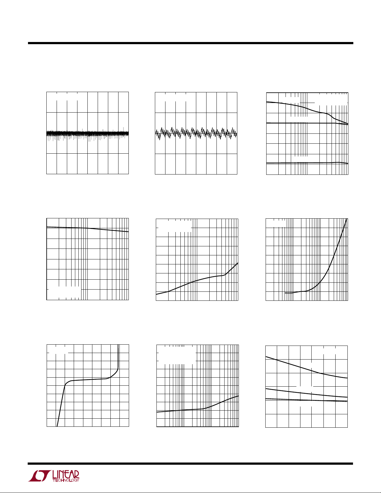
Power Consumption vs Sample Rate
100
3.2MHz CLOCK
= 25°C
T
A
10
1
0.1
SUPPLY CURRENT (mA)
0.01
0.001
0.01
NORMAL CONVERSION
NAP MODE
BETWEEN CONVERSION
SHUTDOWN MODE
BETWEEN CONVERSION
SLEEP MODE BETWEEN
CONVERSION
100
0.1 1
10 1k 1M
SAMPLE RATE (Hz)
10k 100k
LTC1401 • TA02
1
Page 2
LTC1401
TOP VIEW
V
CC
A
IN
V
REF
GND
SHDN
CONV
CLK
D
OUT
S8 PACKAGE
8-LEAD PLASTIC SO
1
2
3
4
8
7
6
5
WW
W
ABSOLUTE MAXIMUM RATINGS
(Notes 1, 2)
Supply Voltage (VCC) ................................................. 7V
Analog Input Voltage (Note 3) ..... –0.3V to (VCC + 0.3V)
Digital Input Voltage (Note 4) ....................–0.3V to 12V
Digital Output Voltage.................. –0.3V to (VCC + 0.3V)
U
U
W
PACKAGE/ORDER INFORMATION
ORDER PART
NUMBER
LTC1401CS8
LTC1401IS8
Power Dissipation.............................................. 300mW
Operating Ambient Temperature Range
LTC1401C................................................0°C to 70°C
LTC1401I............................................ – 40°C to 85°C
T
= 125°C, θJA = 130°C/ W
JMAX
S8 PART MARKING
1401
1401I
Operating Junction Temperature ......................... 125°C
Storage Temperature Range ................. –65°C to 150°C
Consult factory for PDIP packages and Military grade parts.
Lead Temperature (Soldering, 10 sec)..................300°C
U
W
POWER REQUIRE E TS
SYMBOL PARAMETER CONDITIONS MIN TYP MAX UNITS
V
CC
I
CC
P
D
Supply Voltage 2.7 3.0 3.6 V
Supply Current f
Power Dissipation f
(Note 5)
= 200ksps ● 510 mA
SAMPLE
Nap Mode
Sleep Mode
Shutdown Mode ● 4.5 10 µA
= 200ksps ● 15 30 mW
SAMPLE
Nap Mode
Sleep Mode
Shutdown Mode ● 13.5 30 µW
● 0.5 1.0 mA
● 6.5 15 µA
● 1.5 3.0 mW
● 19.5 45 µW
U
IA
U
PUT
(Note 5)
During Conversions (Hold Mode) 5 pF
(Note 5)
= 0 1.180 1.200 1.220 V
OUT
= 0 ● ±10 ±45 ppm/°C
OUT
≤ 1mA 2 LSB/mA
OUT
= 10µF3ms
VREF
U
IN
U
LOG
IN
IN
Analog Input Range ● 0 to 2.048 V
Analog Input Leakage Current During Conversions (Hold Mode) ● ±1 µA
Analog Input Capacitance Between Conversions (Sample Mode) 45 pF
UU
A
SYMBOL PARAMETER CONDITIONS MIN TYP MAX UNITS
V
I
C
I TER AL REFERE CE CHARACTERISTICS
PARAMETER CONDITIONS MIN TYP MAX UNITS
V
Output Voltage I
REF
V
Output Tempco I
REF
V
Line Regulation 2.7V ≤ VCC ≤ 3.6V 0.01 LSB/V
REF
V
Load Regulation 0 ≤ I
REF
V
Wake-Up Time from Sleep or Shutdown Mode C
REF
2
Page 3
LTC1401
U
CO
PARAMETER CONDITIONS MIN TYP MAX UNITS
Resolution (No Missing Codes) ● 12 Bits
Integral Linearity Error (Note 7) ● ±1 LSB
Differential Linearity Error ● ±1 LSB
Offset Error ±6 LSB
Full-Scale Error ±15 LSB
Full-Scale Tempco I
DY
SYMBOL PARAMETER CONDITIONS MIN TYP MAX UNITS
S/(N + D) Signal-to-Noise 50kHz Input Signal ● 65 68 dB
THD Total Harmonic Distortion 50kHz Input Signal ● –72 –65 dB
IMD Intermodulation Distortion f
VERTER
W
U
IC
A
Plus Distortion Ratio 100kHz Input Signal 65 dB
Up to 5th Harmonic 100kHz Input Signal –66 dB
Peak Harmonic or 50kHz Input Signal ● –74 –65 dB
Spurious Noise 100kHz Input Signal –67 dB
Full Power Bandwidth 2 MHz
Full Linear Bandwidth (S/(N + D) ≥ 68dB) 50 kHz
CCHARA TERIST
ACCURACY
(Note 5)
ICS
OUT(REF)
IN1
With internal reference (Note 5)
● ±8 LSB
= 0 ● ±10 ±45 ppm/°C
= 49.853kHz, f
= 53.076kHz –69 dB
IN2
UU
DIGITAL I PUTS AND OUTPUTS
SYMBOL PARAMETER CONDITIONS MIN TYP MAX UNITS
V
IH
V
IL
I
IN
C
IN
V
OH
V
OL
I
OZ
C
OZ
I
SOURCE
I
SINK
High Level Input Voltage V
Low Level Input Voltage VCC = 2.7V ● 0.8 V
Digital Input Current VIN = 0V to V
Digital Input Capacitance 5pF
High Level Output Voltage VCC = 2.7V, IO = –10µA ● 2.40 2.64 V
Low Level Output Voltage VCC = 2.7V, IO = 400µA ● 0.13 0.4 V
Hi-Z Output Leakage D
Hi-Z Output Capacitance D
Output Source Current V
Output Sink Current V
OUT
OUT
(Note 5)
= 3.6V ● 2.0 V
CC
CC
VCC = 2.7V, IO = –200µA ● 2.25 2.50 V
V
= 0V to V
OUT
= 0 –5 mA
OUT
= V
OUT
CC
CC
● ±10 µA
● ±10 µA
15 pF
10 mA
3
Page 4
LTC1401
W
U
TI I G CHARACTERISTICS
SYMBOL PARAMETER CONDITIONS MIN TYP MAX UNITS
f
SAMPLE(MAX)
t
CONV
t
ACQ
f
CLK
t
CLK
t
WK(NAP)
t
1
t
2
t
3
t
4
t
5
t
6
t
7
t
8
t
9
t
10
Maximum Sampling Frequency ● 200 kHz
Conversion Time f
Acquisition Time 315 ns
CLK Frequency ● 0.1 3.2 MHz
CLK Pulse Width (Note 6) ● 60 ns
Time to Wake Up from Nap Mode 350 ns
CLK Pulse Width to Return to Active Mode ● 60 ns
CONV↑ to CLK↑ Setup Time ● 100 ns
CONV↑ After Leading CLK↑ ● 0ns
CONV Pulse Width (Note 8) ● 50 ns
Time from CLK↑ to Sample Mode 80 ns
Aperture Delay of Sample-and-Hold Jitter < 50ps 45 ns
Minimum Delay Between Conversion (Note 6) ● 350 550 ns
Delay Time, CLK↑ to D
Delay Time, CLK↑ to D
Time from Previous Data Remains Valid After CLK↑ C
Valid C
OUT
Hi-Z C
OUT
(Note 5)
= 3.2MHz ● 4.1 µs
CLK
= 20pF ● 60 120 ns
LOAD
= 20pF ● 60 120 ns
LOAD
= 20pF ● 15 50 ns
LOAD
The ● denotes specifications which apply over the full operating
temperature range; all other limits and typicals apply to TA = 25°C.
Note 1: Absolute Maximum Ratings are those values beyond which the life
of a device may be impaired.
Note 2: All voltage values are with respect to GND.
Note 3: When these pin voltages are taken below GND or above V
will be clamped by internal diodes. This product can handle input currents
greater than 40mA without latch-up if the pin is driven below GND or
above VCC.
Note 4: When these pin voltages are taken below GND, they will be clamped
by internal diodes. This product can handle input currents greater than 40mA
without latch-up if the pin is driven below GND. These pins are not clamped
.
to V
CC
CC
, they
Note 5: V
specified.
Note 6: Guaranteed by design, not subject to test.
Note 7: Integral nonlinearity is defined as the deviation of a code from a
straight line passing through the actual endpoints of the transfer curve.
The deviation is measured from the center of the quantization band.
Note 8: The rising edge of CONV starts a conversion. If CONV returns low
at a bit decision point during the conversion, it can create small errors. For
best performance, ensure that CONV returns low either within 120ns after
the conversion starts (i.e., before the first bit decision) or after the 14
clock cycles. (Figure 13 Timing Diagram).
= 3V, f
CC
= 200kHz, tr = tf = 5ns unless otherwise
SAMPLE
4
Page 5
W
INPUT FREQUENCY (kHz)
10
0
SIGNAL/(NOISE + DISTORTION)(dB)
10
20
30
40
80
100 1000
LTC1401 • TPC03
50
60
70
VIN = 0dB
VIN = –20dB
VIN = –60dB
TA = 25°C
f
SAMPLE
= 200kHz
SOURCE RESISTANCE (Ω)
10
2500
t
ACQ
(ns)
3000
3500
4000
4500
100 1k 10k
LTC1401 • TPC06
2000
1500
500
0
1000
TA = 25°C
U
TYPICAL PERFORMANCE CHARACTERISTICS
LTC1401
Differential Nonlinearity vs
Output Code
1.0
f
= 200kHz
SAMPLE
0.5
0
DNL ERROR (LSBs)
–0.5
–1.0
0
512 1024 1536 2048
2560 3072 3584 4096
CODE
Signal-to-Noise Ratio (Without
Harmonics) vs Input Frequency
80
70
60
50
40
30
20
SIGNAL-TO-NOISE RATIO (dB)
10
TA = 25°C
= 200kHz
f
SAMPLE
0
10
INPUT FREQUENCY (kHz)
100 1000
LTC1401 • TPC01
LTC1401 • TPC04
Integral Nonlinearity vs
Output Code
1.0
f
= 200kHz
SAMPLE
0.5
0
INL ERROR (LSBs)
–0.5
–1.0
0
512 1024 1536 2048
2560 3072 3584 4096
CODE
Peak Harmonic or Spurious Noise
vs Input Frequency
0
TA = 25°C
–10
–20
–30
–40
–50
–60
–70
–80
SPURIOUS-FREE DYNAMIC RANGE (dB)
–90
10
= 200kHz
f
SAMPLE
INPUT FREQUENCY (kHz)
100 1000
S/(N + D) vs Input Frequency
and Amplitude
LTC1401 • TPC02
Acquisition Time vs
Source Impedance
LTC1401 • TPC05
Reference Voltage vs
Load Current
1.40
TA = 25°C
1.35
1.30
1.25
1.20
1.15
1.10
1.05
REFERENCE VOLTAGE (V)
1.00
0.95
0.90
–7
–6 –4
–5
–2 2
–3
LOAD CURRENT (mA)
–1
0
1
LTC1401 • TPC07
Power Supply Feedthrough vs
Ripple Frequency
0
f
= 200kHz
SAMPLE
–10
= 49.853kHz
f
IN
(V
V
–20
CC
–30
–40
–50
–60
–70
–80
POWER SUPPLY FEEDTHROUGH (dB)
–90
–100
1
= 1mV)
RIPPLE
10 100 1000
RIPPLE FREQUENCY (kHz)
LTC1401 • TPC08
Supply Current vs Temperature
12
10
8
6
4
SUPPLY CURRENT (mA)
2
0
–50
–25 0
TEMPERATURE (˚C)
f
SAMPLE
VIN = 3.6V
VIN = 3V
VIN = 2.7V
50 100 125
25 75
= 200kHz
LTC1401 • TPC09
5
Page 6
LTC1401
PIN FUNCTIONS
UUU
V
(Pin 1): Positive Supply, 3V. Bypass to GND (10µF
CC
tantalum in parallel with 0.1µF ceramic).
AIN (Pin 2): Analog Input. 0V to 2.048V.
V
(Pin 3): 1.2V Reference Output. Bypass to GND
REF
(10µF tantalum in parallel with 0.1µF ceramic).
GND (Pin 4): Ground. GND should be tied directly to an
analog ground plane.
D
(Pin 5): The A/D conversion result is shifted out from
OUT
this pin.
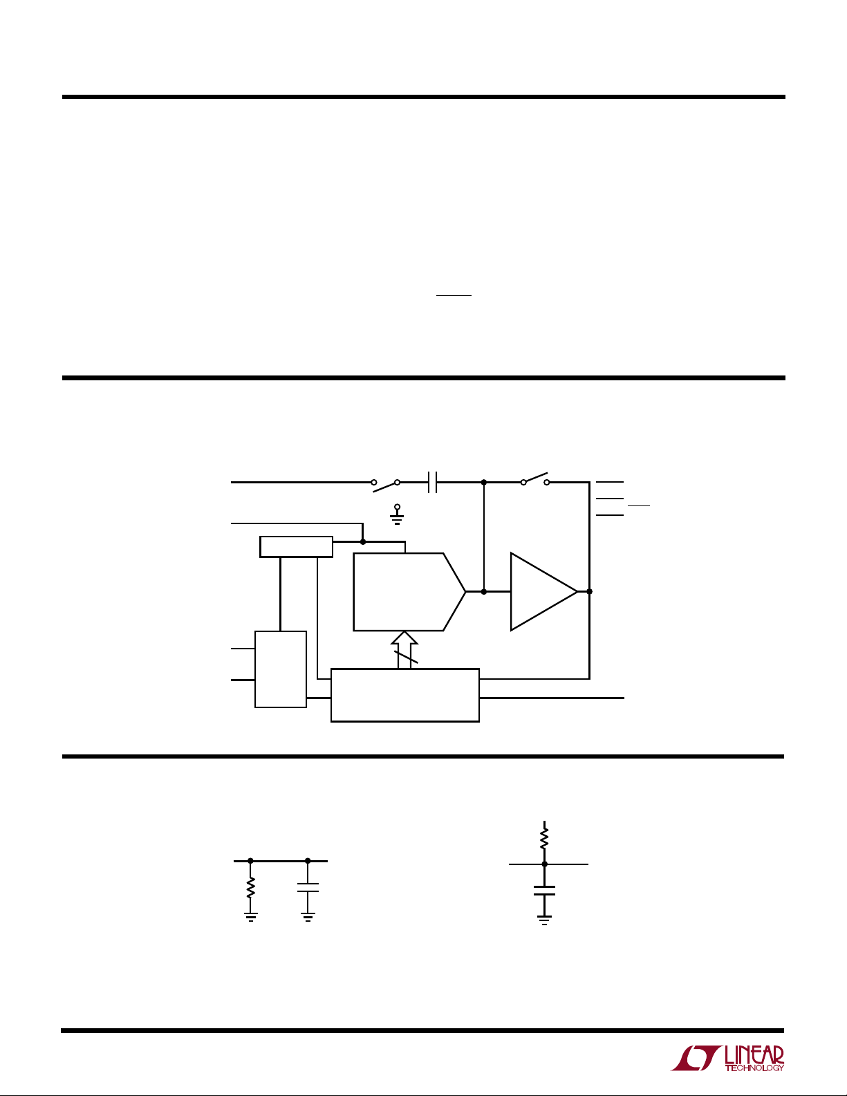
UU
W
FUNCTIONAL BLOCK DIAGRA
A
IN
V
REF
1.20V REF
CLK (Pin 6): Clock. This clock synchronizes the serial data
transfer. A minimum CLK pulse of 60ns signals the ADC to
wake up from Nap or Sleep mode.
CONV (Pin 7): Conversion Start Signal. This active high
signal starts a conversion on its rising edge. Keeping CLK
low and pulsing CONV two/four times will put the ADC into
Nap/Sleep mode.
SHDN (Pin 8): Shutdown Input. Pull this pin Low to put the
ADC in Shutdown mode and save power (REFRDY will go
Low). The device will draw 4.5µA in this mode.
C
SAMPLE
ZEROING SWITCH
V
CC
GND
SHDN
TEST CIRCUITS
CLK
CONV
D
OUT
CONTROL
LOGIC
3k
Hi-Z TO V
V
OL TO VOH
V
TO Hi-Z
OH
12-BIT CAPACITIVE DAC COMP
12
SUCCESSIVE APPROXIMATION
REGISTER/PARALLEL TO
SERIAL CONVERTER
3V
3k
D
OUT
C
LOAD
OH
Hi-Z TO V
V
OH TO VOL
V
TO Hi-Z
OL
C
LOAD
OL
LTC1401 • TC01
D
OUT
LTC1401 • BD01
6
Page 7

LTC1401
FREQUENCY (kHz)
0204050709010 30 60 80 100
AMPLITUDE (dB)
LTC1401 • F02a
0
–10
–20
–30
–40
–50
–60
–70
–80
–90
–100
–110
–120
f
SAMPLE
= 200kHz
f
IN
= 49.853516kHz
SINAD = 68.5dB
THD = –72.4dB
V
CC
= 3V
T
A
= 25°C
U
WUU
APPLICATIONS INFORMATION
Conversion Details
The LTC1401 uses a successive approximation algorithm
and an internal sample-and-hold circuit to convert an
analog signal to a 12-bit serial output based on a precision
internal reference. The control logic provides an easy
interface to microprocessors and DSPs through serial
3-wire connections.
A rising edge on the CONV input starts a conversion. At the
start of a conversion the successive approximation register (SAR) is reset. Once a conversion cycle has begun, it
cannot be restarted.
During conversion, the internal 12-bit capacitive DAC
output is sequenced by the SAR from the most significant
bit (MSB) to the least significant bit (LSB). Referring to
Figure 1, the AIN input connects to the sample-and-hold
capacitor during the acquire phase and the comparator
offset is nulled by the feedback switch. In this acquire
phase, it typically takes 315ns for the sample-and-hold
capacitor to acquire the analog signal. During the convert
phase, the comparator feedback switch opens, putting the
comparator into the compare mode. The input switches
C
SAMPLE
the summing junction. This input charge is successively
compared with the binary-weighted charges supplied by
the capacitive DAC. Bit decisions are made by the high
speed comparator. At the end of a conversion, the DAC
to ground, injecting the analog input charge onto
SAMPLE
output balances the AIN input charge. The SAR contents (a
12-bit data word) which represent the input voltage, are
presented through the serial pin D
OUT
.
Dynamic Performance
The LTC1401 has excellent high speed sampling capability. FFT (Fast Fourier Transform) test techniques are used
to test the ADC’s frequency response, distortion and noise
at the rated throughput. By applying a low distortion sine
wave and analyzing the digital output using an FFT algorithm, the ADC’s spectral content can be examined for
frequencies outside the fundamental. Figure 2a shows a
typical LTC1401 FFT plot.
Figure 2a. LTC1401 Nonaveraged, 4096 Point FFT
Plot with 50kHz Input Frequency
SAMPLE
A
IN
HOLD
C
SAMPLE
DAC
C
DAC
V
DAC
Figure 1. AIN Input
S1
–
+
COMP
Signal-to-Noise Ratio
The signal-to-noise plus distortion ratio [S/(N+D)] is the
ratio between the RMS amplitude of the fundamental input
frequency to the RMS amplitude of all other frequency
S
A
R
D
OUT
LTC1401 • F01
components at the A/D output. The output is band limited
to frequencies from DC to half the sampling frequency.
Figure 2a shows a typical spectral content with a 200kHz
sampling rate and a 50kHz input. The dynamic performance is excellent for input frequencies up to the Nyquist
limit of 100kHz as shown in Figure 2b.
7
Page 8

LTC1401
INPUT FREQUENCY (Hz)
10k
AMPLITUDE (dB BELOW THE FUNDAMENTAL)
0
–10
–20
–30
–40
–50
–60
–70
–80
–90
–100
100k 1M
LTC1401 • F04
2ND HARMONIC
THD
3RD HARMONIC
TA = 25°C
f
SAMPLE
= 200kHz
U
WUU
APPLICATIONS INFORMATION
0
f
= 200kHz
SAMPLE
–10
= 99.072266kHz
f
IN
–20
SINAD = 65dB
THD = –66dB
–30
= 3V
V
CC
–40
= 25°C
T
A
–50
–60
–70
AMPLITUDE (dB)
–80
–90
–100
–110
–120
0204050709010 30 60 80 100
Figure 2b. LTC1401 Nonaveraged, 4096 Point FFT
Plot with 100kHz Input Frequency
Effective Number of Bits
The effective number of bits (ENOBs) is a measurement of
the effective resolution of an ADC and is directly related to
the S/(N + D) by the equation:
FREQUENCY (kHz)
LTC1400 • F02b
Total Harmonic Distortion
Total harmonic distortion (THD) is the ratio of the RMS
sum of all harmonics of the input signal to the fundamental
itself. The out-of-band harmonics alias into the frequency
band between DC and half of the sampling frequency. THD
is expressed as:
2
THD = 20log
√
V22 + V32 + ...Vn
V1
Where V1 is the RMS amplitude of the fundamental
frequency and V2 through Vn are the amplitudes of the
second through nth harmonics. THD vs input frequency is
shown in Figure 4. The LTC1401 has good distortion
performance up to the Nyquist frequency and beyond.
SN D
+
/–.
N
()
=
.
602
where N is the effective number of bits of resolution and
S/(N + D) is expressed in dB. Figure 3 shows ENOBs vs
Input Frequency.
12
11
10
9
8
7
6
5
4
3
EFFECTIVE NUMBER OF BITS
2
TA = 25°C
1
f
SAMPLE
8
0
10k
Figure 3. Effective Bits and Signal-to-Noise +
Distortion vs Input Frequency
176
= 200kHz
100k 1M
INPUT FREQUENCY (Hz)
LTC1401 • F03
74
68
SIGNAL/(NOISE + DISTORTION) (dB)
62
56
50
Intermodulation Distortion
If the ADC input signal consists of more than one spectral
component, the ADC transfer function nonlinearity can
produce intermodulation distortion (IMD) in addition to
THD. IMD is the change in one sinusoidal input caused by
the presence of another sinusoidal input at a different
frequency.
If two pure sine waves of frequencies fa and fb are applied
to the ADC input, nonlinearities in the ADC transfer
function can create distortion products at sum and differ-
Figure 4. Distortion vs Input Frequency
Page 9

LTC1401
U
WUU
APPLICATIONS INFORMATION
ence frequencies of mfa ±nfb, where m and n = 0, 1, 2, 3,
etc. For example, the 2nd order IMD terms include (fa + fb)
and (fa – fb) while 3rd order IMD terms includes
(2fa + fb), (2fa – fb), (fa + 2fb) and (fa – 2fb). If the two input
sine waves are equal in magnitude, the value (in decibels)
of the 2nd order IMD products can be expressed by the
following formula.
fa fb
IMD fa fb
±
()
=
Amplitude at ( )
20log
Amplitude at fa
Figure 5 shows the IMD performance at a 50kHz input.
0
f
= 200kHz
SAMPLE
–10
fa = 49.853kHz
–20
fb = 53.076kHz
= 25°C
T
–30
A
–40
–50
–60
–70
AMPLITUDE (dB)
–80
–90
–100
–110
–120
Figure 5. Intermodulation Distortion Plot
2fa – fb
2fb + fa
fb – fa
0204050709010 30 60 80 100
fa fb
3fb
FREQUENCY (kHz)
2fa + fb
3fa
2fb – fa
fa + fb
2fb
Peak Harmonic or Spurious Noise
The peak harmonic or spurious noise is the largest spectral component excluding the input signal and DC. This
value is expressed in decibels relative to the RMS value of
a full-scale input signal.
Full Power and Full Linear Bandwidth
The full power bandwidth is the input frequency at which
the amplitude of the reconstructed fundamental is reduced
by 3dB for a full-scale input signal.
The full linear bandwidth is the input frequency at which
the S/(N+D) has dropped to 68dB (11 effective bits).
±
2fa
LTC1401 • F05
Driving the Analog Input
The analog input of the LTC1401 is easy to drive. It draws
only one small current spike while charging the sampleand-hold capacitor at the end of a conversion. During
conversion, the analog input draws only a small leakage
current. The only requirement is that the amplifier driving
the analog input must settle after the small current spike
before the next conversion starts. Any op amp that settles
in 315ns to small load current transients will allow maximum speed operation. If a slower op amp is used, more
settling time can be provided by increasing the time
between conversions. Suitable devices capable of driving
the ADC’s AIN input include the LT®1498 and the LT1630
op amps.
The following
list is a summary of the op amps that are
suitable for driving the LTC1401, more detailed information is available in the Linear Technology databooks and
the LinearViewTM CD-ROM.
LT1215/LT1216: Dual and quad 23MHz, 50V/µs single
supply op amps. Single 5V to ±15V supplies, 6.6mA
specifications, 90ns settling to 0.5LSB.
LT1229/LT1230: Dual and quad 100MHz current feedback
amplifiers. ±2V to ± 15V supplies, 6mA supply current
each amplifier. Low noise. Good AC specs.
LT1498/LT1499: Dual or quad 10MHz, 6V/µs, single
2.2V to ±15V supplies, 1.7mA supply current per amplifier, input/output swings rail-to-rail. Excellent AC and DC
specs.
LT1630: Dual or quad 30MHz, 10V/µ s, single 2.7V to ±15V
supplies, 3.5mA supply current per amplifier, input/output
swings rail-to-rail. Good AC and DC specs.
Internal Reference
The LTC1401 has an on-chip, temperature compensated,
curvature corrected, bandgap reference, which is factory
trimmed to 1.20V. It is internally connected to the DAC and
LinearView is a trademark of Linear Technology Corporation.
9
Page 10

LTC1401
U
WUU
APPLICATIONS INFORMATION
is available at Pin 3 to provide up to 1mA current to an
external load. For minimum code transition noise, the
reference output should be decoupled with a capacitor to
filter wideband noise from the reference (10uF tantalum in
parallel with a 0.1uF ceramic is recommended). The V
pin can be driven with a DAC or other means to provide
input span adjustment. The V
pin must be driven to at
REF
least 1.25V to prevent conflict with the internal reference.
The reference should not be driven to more than 3V.
Figure 6 shows an LT1360 op amp driving the reference
pin. Figure 7 shows a typical reference (LT1634-1.25)
connected to the LTC1401. This will provide improved
drift (equal to the maximum 25ppm/°C of the LT1634-
1.25) and a 2.1338V full scale.
INPUT RANGE
1.707 • V
REF(OUT)
Figure 6. Driving the V
INPUT RANGE 1.707 • V
(= 2.1338V)
+
LT1360
–
REF
LT1634-1.25
V
≥ 1.25V
REF(OUT)
3Ω
with the LT1360 Op Amp
REF
10V
V
IN
V
OUT
3Ω
10µF
GND
10µF
A
IN
LTC1401
V
REF
GND
A
IN
V
REF
GND
3V
V
CC
LTC1401 • F06
3V
V
CC
LTC1401
LTC1401 • F07
REF
UNIPOLAR OPERATION AND ADJUSTMENT
Figure 8 shows the ideal input/output characteristics for
the LTC1401. The code transitions occur midway between
successive integer LSB values (i.e., 0.5LSB, 1.5LSB,
2.5LSB, ... FS – 1.5LSB ). The output code is natural binary
with 1LSB = 2.048/4096 = 0.5mV.
111...111
111...110
111...101
111...100
OUTPUT CODE
000...011
000...010
000...001
000...000
0V
1LSB =
UNIPOLAR
ZERO
1
LSB
=
4096
4096
INPUT VOLTAGE (V)
FS – 1LSB
LTC1401 • F08
2.048
FS
Figure 8. LTC1401 Unipolar Transfer Characteristics
Unipolar Offset and Full-Scale Error Adjustments
In applications where absolute accuracy is important, the
offset and full-scale errors can be adjusted to zero. Offset
error must be adjusted before full-scale error. Figure 9a
shows the extra components required for full scale error
adjustment. If both offset and full-scale adjustments are
needed, the circuit in Figure 9b can be used. For zero offset
error, apply 0.25mV (i.e., 0.5LSB) at the input and adjust
the offset trim until the LTC1401 output code flickers
between 0000 0000 0000 and 0000 0000 0001. For zero
full-scale error, apply an analog input of 2.04725V ( FS –
1.5LSB or last code transition ) at the input and adjust R5
until the LTC1401 output code flickers between 1111 1111
1110 and 1111 1111 1111.
10
Figure 7. Supplying a 2.5V Reference Voltage to
the LTC1401 with the LT1634-1.25
Page 11

LTC1401
ANALOG SUPPLY
GND 3V
+
LTC1401
V
CC
GND
DIGITAL SUPPLY
GND 3V
+
DIGITAL CIRCUITRY
V
CC
GND
LTC1401 • F10
U
WUU
APPLICATIONS INFORMATION
R1
50Ω
V
IN
R2
10k
ADDITIONAL PINS OMITTED FOR CLARITY
±20LSB TRIM RANGE
Figure 9a. LTC1401 Full-Scale Adjust Circuit
R1
ANALOG
INPUT
0V TO 2.048V
10k
10k
3V
R2
10k
R9
20Ω
R3
10k
+
A1
–
R4
100Ω
FULL-SCALE
ADJUST
A
IN
LTC1401
GND
LTC1401 • F09a
+
A1
–
R4
100k
R5
4.3k
FULL-SCALE
ADJUST
R3
100k
R6
400Ω
A
R7
100k
IN
LTC1401
3V
R8
10k
OFFSET
ADJUST
optimum performance, a 10µ F surface mount AVX capacitor in parallel with a 0.1µ F ceramic is recommended for the
VCC and V
pins. The capacitors must be located as close
REF
to the pins as possible. The traces connecting the pins and
the bypass capacitors must be kept short and should be
made as wide as possible.
Input signal leads to AIN and signal return leads from GND
(Pin 4) should be kept as short as possible to minimize
noise coupling. In applications where this is not possible,
a shielded cable between the analog input signal and the
ADC is recommended. Also, any potential difference in
grounds between the analog signal and the ADC appears
as an error voltage in series with the analog input signal.
Attention should be paid to reducing the ground circuit
impedance as much as possible.
Figure 10 shows the recommended system ground connections. All analog circuitry grounds should be terminated at the LTC1401 GND pin. The ground return to the
power supply from Pin 4 should be low impedance for
noise free operation. Digital circuitry grounds must be
connected to the digital supply common.
Figure 9b. LTC1401 Offset and Full-Scale Adjust Circuit
BOARD LAYOUT AND BYPASSING
Wire wrap boards are not recommended for high resolution or high speed A/D converters. To obtain the best
performance from the LTC1401, a printed circuit board is
required. Layout for the printed circuit board should
ensure that digital and analog signal lines are separated as
much as possible. In particular, care should be taken not
to run any digital traces alongside an analog signal trace
or underneath the ADC. The analog input should be
screened by GND.
High quality tantalum and ceramic bypass capacitors
should be used at the VCC and V
Typical Application on the first page of this datasheet. For
LTC1401 • F09b
Figure 10. Power Supply Connection
Power-Down Mode
Upon power up, the LTC1401 is initialized to the active
state and is ready for conversion. However, the chip can be
easily placed into Nap or Sleep mode by exercising the
right combination of CLK and CONV signals. In Nap mode,
pins as shown in the
REF
all power is off except the internal reference which remains
active and provides 1.20V output voltage to the other
11
Page 12

LTC1401
U
WUU
APPLICATIONS INFORMATION
circuitry. In this mode, the ADC draws only 1.5mW of
power instead of 15mW (for minimum power, the logic
inputs must be within 500mV of the supply rails). The
wake-up time from Nap mode to active mode is 350ns. In
Sleep mode, power consumption is reduced to 19.5µ W by
cutting off the supply to the comparator and reference.
Figure 11 illustrates power-down methods for the LTC1401.
The chip enters Nap mode by keeping the CLK signal low
and pulsing the CONV signal twice. For Sleep mode
operation, CONV signal should be pulsed four times while
CLK is kept low. NAP and SLEEP modes are activated on
the falling edge of the CONV pulse. By pulling SHDN low,
the LTC1401 enters Shutdown mode and power consumption drops to 13.5µW.
Once SHDN goes high, the LTC1401 returns to active
mode or the LTC1401 returns to active mode by pulsing
the CLK signal if the device has entered Nap/Sleep mode.
During the transistion from Sleep mode to active mode,
the V
conditions. With a 10µF bypass capacitor, the wake-up
time from Sleep mode is typically 3ms. A REFRDY signal
is activated once the reference has settled and is ready for
voltage ramp-up time is a function of its loading
REF
an A/D conversion. This REFRDY bit is sent to the D
OUT
pin
as the first bit followed by the 12-bit data word (refer to
Figure 12).
DIGITAL INTERFACE
The digital interface requires only three digital lines. CLK
and CONV are both inputs, and the D
output provides
OUT
the conversion result in serial form.
Figures 12 and 13 show the digital timing waveform of the
LTC1401 during the Analog to Digital Conversion. The
CONV rising edge starts the conversion. Once initiated, it
can not be restarted until the conversion is completed. If
the time from the CONV signal to the CLK rising edge is
less than t2, the digital output will be delayed by one clock
cycle.
The digital output data is updated on the rising edge of the
CLK line. The digital output data consists of a REFRDY bit
followed by the valid 12-bit data word. D
data should
OUT
be captured by the receiving system on the rising CLK
edge. Data remains valid for a minimum time of t10 after
the rising CLK edge to allow capture to occur.
CLK
CONV
NAP
SLEEP
V
REF
REFRDY
t
1
NOTE: NAP AND SLEEP ARE INTERNAL SIGNALS. REFRDY APPEARS AS THE FIRST BIT IN THE D
Figure 11. Nap Mode and Sleep Mode Waveforms
t
1
LTC1401 • F11
WORD.
OUT
12
Page 13

LTC1401
U
WUU
APPLICATIONS INFORMATION
t
2
t
3
CLK
CONV
INTERNAL
S/H STATUS
D
OUT
SAMPLE SAMPLEHOLD HOLD
123456789101112131415 16 1 2
t
4
t
6
Hi-Z Hi-Z
REFRDY D11 D9 D 8 D7 D6 D 5 D 4 D3 D2 D1 D0D10
REFRDY BIT + 12-BIT DATA WORD
t
CONV
t
SAMPLE
t
7
t
5
t
ACQ
t
8
REFRDY
LT1401 • F12
CLK
D
OUT
t
8
t
10
Figure 12. ADC Digital Timing Waveform
V
IH
Figure 13. CLK to D
V
OH
V
OL
CLK
D
OUT
OUT
Delay
V
IH
t
9
90%
10%
LTC1401 • F13
13
Page 14

LTC1401
TYPICAL APPLICATIONS
Interface to the TMS320C50’s TDM Serial Port (Frame Sync is Generated from TFSX)
U
5V
3V
8
1
+
10µF
0.1µF
UNIPOLAR
+
10µF
2
INPUT
3
0.1µF
SHDN
V
CC
LTC1401
A
IN
V
REF
GND
CLK
CONV
D
OUT
4
2.5MHz EXTERNAL CLOCK
TMS320C50
6
7
5
TCLKX
TCLKR
TFSX
TFSR
TDR
CLK
20MHz
OUT
CLR
LD P T
QC
74HC161
CLK A B C D
LTC1401 • TA04a
Logic Analyzer Waveforms Show 6.4µs Throughput Rate (Input Voltage = 0.765V, Output Code = 0101 1111 1010 = 153010)
14
1401 TA5b
Data from the LTC1401 Loaded into the TMS320C50’s TRCV Register
D0 X
RDYXD11
D10 D9
D4
D5 D3
D7 D6
D8
D1
D2
X
1401 TA4c
Data Stored in the TMS320C50’s Memory (in Right Justified Format)
D2 D1
000
RDY D11
D10
D9 D8
D6
D7 D5
D3
D4
D0
1401 TA4d
Page 15

U
TYPICAL APPLICATIONS
TMS320C50 Code for Circuit
THIS PROGRAM DEMONSTRATES THE LTC1401 INTERFACE TO THE
TMS320C50. FRAME SYNC PULSE IS GENERATED FROM TFSX.
DATA SHIFT CLOCK IS DERIVED FROM CLKOUT.
*Initialization*
.mmregs ; Defines global symbolic names
;- - Initialized data memory to zero
.ds 0F00h ; Initialize data to zero
DATA0 .word 0 ; Begin sample data location
DATA1 .word 0 ; .
DATA2 .word 0 ; Location of data
DATA3 .word 0 ; .
DATA4 .word 0 ; .
DATA5 .word 0 ; End sample data location
;- - Set up the ISR vector
.ps 080Ah ; Serial ports interrupts
rint : B RECEIVE ; 0A;
xint : B TRANSMIT ; 0C;
trnt : B TREC ; 0E;
txnt : B TTRANX ; 10;
;- - Setup the reset vector
.ps 0A00h
.entry
START:
*TMS320C50 Initialization*
SETC INTM ; Temporarily disable all interrupts
LDP #0 ; Set data page pointer to zero
OPL #0834h, PMST ; Set up the PMST status and control register
LACC #0
SAMMCWSR ; Set software wait state to 0
SAMMPDWSR ;
*Configure Serial Port*
SPLK #0028h, TSPC ; Set TDM Serial Port
; TDM = 0 Stand Alone mode
; DLB = 0 Not loop back
; FO = 0 16 Bits
; FSM = 1 Burst Mode
; MCM = 0 CLKR is generated externally
; TXM = 1 FSX as output pin
; Put serial port into reset
; (XRST = RRST = 0)
SPLK #00E8h, TSPC ; Take Serial Port out of reset
; (XRST = RRST = 1)
SPLK #0FFFFh, IFR ; Clear all the pending interrupts
LTC1401
*Start Serial Communication*
SACL TDXR ; Generate frame sync pulse
SPLK #040h, IMR ; Turn on TRNT receiver interrupt
CLRC INTM ; Enable interrupt
CLRC SXM ; For Unipolar input, set for right shift
MAR *AR7 ; Load the auxiliary register pointer with seven
LAR AR7, #0F00h ; Load the auxiliary register seven with #0F00h
WAIT: NOP ; Wait for a receive interrupt
; - - - - - - - end of main program - - - - - - - - - - ;
*Receiver Interrupt Service Routine*
TREC:
*After Obtained the Data from LTC1401, Program Jump to END_TRCV*
END_TRCV:
SUCCESS:
*Fill the unused interrupt with RETE, to avoid program get “lost”*
TTRANX:
RECEIVE:
TRANSMIT:
INT2:
NOP ;
NOP ;
SACL TDXR ; !! Regenerate the frame sync pulse
B WAIT ;
LAMM TRCV ; Load the data received from LTC1401
SFR ; Shift right two times
SFR ;
AND #1FFFh, 0 ; ANDed with #1FFFh
SACL *+, 0 ; Write to data memory pointed by AR7 and
LACC AR7 ;
SUB #0F05h,0 ; Compare to end sample address #0F05h
END_TRCV, GEQ
BCND
SPLK #040h, IMR ; Else re-enable the TRNT receive interrupt
RETE ; Return to main program and enable interrupt
SPLK #002h, IMR ; Enable INT2 for program to halt
CLRC INTM
B SUCCESS
RETE
RETE
RETE
B halt ; Halts the running CPU
; with no sign extension
; as the begin address for data storage
; For converting the data to right
; justified format
;
; Increase the memory address by one
; If the end sample address has exceeded jump
to END_TRCV
;
15
Page 16

LTC1401
TYPICAL APPLICATIONS
LTC1401 Interface to the ADSP2181’s SPORT0 (Frame Sync is Generated from RFS)
U
3V
8
1
2
INPUT
3
0.1µF
+
10µF
0.1µF
+
UNIPOLAR
10µF
SHDN
V
CC
LTC1401
A
IN
V
REF
GND
CLK
CONV
D
OUT
6
7
5
ADSP2181
SCLKO
RFS
DR0
LTC1401 • TA05a
Logic Analyzer Waveforms Show 4.8µs Throughput Rate (Input Voltage = 1.604V, Output Code = 1100 1000 1000 = 320810)
16
1401 TA04b
Data from the LTC1401 (Normal Mode)
RDYXD11
D10 D9
D4
D7 D6
D8
D5 D3
D2
D0 X
D1
X
LTC1401 • TA05c
Data Stored in the ADSP2181’s Memory (Normal Mode, SLEN = D)
000
RDY D11
D10
D9 D8
D6
D7 D5
D4
D3
D2 D1
D0
LTC1401 • TA05d
Page 17

U
TYPICAL APPLICATIONS
LTC1401
ADSP2181 Code for Circuit
THIS PROGRAM DEMONSTRATES THE LTC1401 INTERFACE TO THE
ADSP-2181. FRAME SYNC PULSE IS GENERATED FROM RFS.
DATA SHIFT CLOCK IS INTERNALLY GENERATED.
/*Section 1: Initialization*/
.module/ram/abs = 0 adspltc; /*define the program module*/
jump start; /*jump over interrupt vectors*/
nop; nop; nop;
rti; rti; rti; rti; /*code vectors here upon IRQ2 int*/
rti; rti; rti; rti; /*code vectors here upon IRQL1 int*/
rti; rti; rti; rti; /*code vectors here upon IRQL0 int*/
rti; rti; rti; rti; /*code vectors here upon SPORT0 TX int*/
ax0 = rx0; /*Section 5*/
dm (0x2000) = ax0; /*begin of SPORT0 receive interrupt*/
rti; /* */
/* */
rti; rti; rti; rti; /*code vectors here upon /IRQE int*/
rti; rti; rti; rti; /*code vectors here upon BDMA interrupt*/
rti; rti; rti; rti; /*code vectors here upon SPORT1 TX (IRQ1) int*/
rti; rti; rti; rti; /*code vectors here upon SPORT1 RX (IRQ0) int*/
rti; rti; rti; rti; /*code vectors here upon TIMER int*/
rti; rti; rti; rti;
/*Section 2: Configure SPORT0*/
start:
/*to configure SPORT0 control reg*/
ax0 = 0x6F0D;
dm (0x3FF6) =ax0;
/*end of SPORT0 receive interrupt*/
/*code vectors here upon POWER DOWN int*/
/*SPORT0 address = 0x3FF6*/
/*RFS is used for frame sync generation*/
/*RFS is internal, TFS is not used*/
/*bit 0-3 = Slen*/
/*F = 15 = 1111*/
/*E = 14 = 1110*/
/*D = 13 = 1101*/
/*bit 4,5 data type right justified zero filled MSB*/
/*bit 6 INVRFS = 0*/
/*bit 7 INVTFS = 0*/
/*bit 8 IRFS=1 receive internal frame sync*/
/*bit 9,10,11 are for TFS (don’t care)*/
/*bit 12 RFSW=0 receive is normal mode*/
/*bit 13 RTFS=1 receive is framed mode*/
/*bit 14 ISCLK = 1 clock is internal*/
/*bit 15 multichannel mode = 0*/
/*Section 3: configure CLKDIV and RFSDIV, setup interrupts*/
/*to configure CLKDIV reg*/
ax0= 4;
dm(0x3FF5) =ax0; /*set the serial clock divide modulus reg
SCLKDIV*/
/*the input clock frequency = 16.67MHz*/
/*CLKOUT frequency = 2x = 33MHz*/
/*SCLK= 1/2*CLKOUT*1/(SCLKDIV+1)*/
/*for SCLKDIV = 4, SCLK = 33/10 = 3.3MHz*/
/*to Configure RFSDIV*/
ax0 = 15; /*set the RFSDIV reg = 15*/
/*=> the frame sync pulse for every 16 SCLK*/
/*if frame sync pulse in every 15 SCLK, ax0=14*/
dm(0x3FF4) =ax0;
/*to setup interrupt*/
ifc= 0x0066; /*clear any extraneous SPORT interrupts*/
icntl= 0; /*IRQXB = level sensitivity*/
/*disable nesting interrupt*/
imask= 0x0020; /*bit 0 = timer int = 0*/
/*bit 1 = SPORT1 or IRQ0B int = 0*/
/*bit 2 = SPORT1 or IRQ1B int = 0*/
/*bit 3 = BDMA int = 0*/
/*bit 4 = IRQEB int = 0*/
/*bit 5 = SPORT0 receive int = 1*/
/*bit 6 = SPORT0 transmit int = 0*/
/*bit 7 = IRQ2B int = 0*/
/*enable SPORT0 receive interrupt*/
/*Section 4: Configure System Control Register and Start Communication*/
/*to configure system control reg*/
ax0 = dm(0x3FFF); /*read the system control reg*/
ay0 = 0xFFF0;
ar = ax0 AND ay0; /*set wait state to zero*/
ay0 = 0x1000;
ar = ar OR ay0; /*bit 12 = 1, enable SPORT0*/
dm(0x3FFF) = ar;
/*frame sync pulse regenerated automatically*/
cntr = 5000;
do waitloop until ce;
nop;
nop;
nop;
nop;
nop;
nop;
waitloop: nop;
rts;
.endmod;
17
Page 18

LTC1401
TYPICAL APPLICATIONS
Quick Look Circuit for Converting Data to Parallel Format
U
1.20V
REFERENCE
OUTPUT
1
0.1µF
V
CC
LTC1401
2
A
IN
3
V
REF
4
GND
3V
+
10µF
ANALOG INPUT
(0V TO 2.048V)
+
10µF
0.1µF
SHDN
CONV
CLK
D
OUT
8
7
6
5
3-WIRE SERIAL
INTERFACE LINK
CONV
CLK
5V
SRCLR
12
RCK
11
SRCK
74HC595
14
SER
13
G
SRCLR
12
RCK
11
SRCK
74HC595
14
SER
13
G
QA
QB
QC
QD
QE
QG
QH
QH'
QA
QB
QC
QD
QE
QG
QH
QH'
15
D0
1
D1
2
D2
3
D3
4
D4
5
QF
D5
6
D6
7
D7
9
15
D8
1
D9
2
D10
3
D11
4
REFRDY
5
QF
6
7
9
LTC1401 • TA03
18
Page 19

PACKAGE DESCRIPTION
U
Dimensions in inches (millimeters) unless otherwise noted.
S8 Package
8-Lead Plastic Small Outline (Narrow 0.150)
(LTC DWG # 05-08-1610)
0.189 – 0.197*
(4.801 – 5.004)
7
8
5
6
LTC1401
0.228 – 0.244
(5.791 – 6.197)
0.010 – 0.020
(0.254 – 0.508)
0.008 – 0.010
(0.203 – 0.254)
*
DIMENSION DOES NOT INCLUDE MOLD FLASH. MOLD FLASH
SHALL NOT EXCEED 0.006" (0.152mm) PER SIDE
**
DIMENSION DOES NOT INCLUDE INTERLEAD FLASH. INTERLEAD
FLASH SHALL NOT EXCEED 0.010" (0.254mm) PER SIDE
× 45°
0°– 8° TYP
0.016 – 0.050
0.406 – 1.270
0.053 – 0.069
(1.346 – 1.752)
0.014 – 0.019
(0.355 – 0.483)
0.150 – 0.157**
(3.810 – 3.988)
1
3
2
4
0.004 – 0.010
(0.101 – 0.254)
0.050
(1.270)
TYP
SO8 0996
Information furnished by Linear Technology Corporation is believed to be accurate and reliable.
However, no responsibility is assumed for its use. Linear Technology Corporation makes no representation that the interconnection of its circuits as described herein will not infringe on existing patent rights.
19
Page 20

LTC1401
TYPICAL APPLICATIONS
Interface to the TMS320C50’s TDM Serial Port (Frame Sync is Generated from TFSX)
U
5V
LTC1401 Interface to the ADSP2181’s SPORT0 (Frame Sync is Generated from RFS)
RELATED PARTS
3V
8
SHDN
1
V
CC
LTC1401
+
10µF
+
0.1µF
+
UNIPOLAR
10µF
3V
10µF
2
A
0.1µF
10µF
IN
3
V
REF
UNIPOLAR
INPUT
INPUT
0.1µF
+
0.1µF
GND
CONV
D
4
1
V
CC
2
A
IN
3
V
REF
CLK
OUT
6
7
5
8
SHDN
LTC1401
GND
2.5MHz EXTERNAL CLOCK
TMS320C50
TCLKX
TCLKR
TFSX
TFSR
TDR
6
CLK
CONV
D
OUT
SCLKO
7
RFS
5
DR0
CLK
OUT
20MHz
ADSP2181
LTC1401 • TA05a
CLR
LD P T
QC
74HC161
CLK A B C D
LTC1401 • TA04a
12-Bit Parallel Output ADCs
PART NUMBER DESCRIPTION COMMENTS
LTC1273/LTC1275/LTC1276 Complete 5V Sampling 12-Bit ADCs with 70dB SINAD at Niquist Lower Power and Cost Effective for
≤ 300ksps
f
SAMPLE
LTC1274/LTC1277 Low Power 12-Bit ADCs with Nap and Sleep Mode Shutdown Lowest Power (10mW) f
SAMPLE
≤ 100ksps
LTC1278/LTC1279 High Speed Sampling 12-Bit ADCs with Shutdown Cost Effective 12-Bit ADCs with Convert Start Input
Best for 300ksps < f
SAMPLE
≤ 600ksps
LTC1282 Complete 3V 12-Bit ADCs with 12mW Power Dissipation Fully Specified for 3V Powered Applications,
f
≤ 140ksps
SAMPLE
LTC1409 Low Power 12-Bit, 800ksps Sampling ADC Best Dynamic Performance
f
≤ 800ksps, 80mW Dissipation
SAMPLE
LTC1410 12-Bit, 1.25Msps Sampling ADC with Shutdown Best Dynamic Performance, THD = –84dB and
SINAD = 71dB at Nyquist
12-Bit Serial Output ADCs
PART NUMBER V
CC
LTC1285/LTC1288 3V 7.5/6.6ksps 0.48mW 3V, One or Two Input, Micropower, SO-8
LTC1286/LTC1298 5V 12.5/11.1ksps 1.25mV One or Two Input, Micropower, SO-8
LTC1290 5/±5V 50ksps 30mW 8 Input, Full-Duplex Serial I/O
LTC1296 5/±5V 46.5ksps 30mW 8 Input, Half-Duplex Serial I/O, Power Shutdown Output
LTC1400 5/±5V 400ksps 75mW Complete 12-Bit, 400ksps, SO-8 ADC with Shutdown
LTC1404 5/±5V 600ksps 75mW Complete 12-Bit, 600ksps, SO-8 ADC with Shutdown
SAMPLE RATE POWER DISSIPATION DESCRIPTION
20
Linear T echnolog y Corporation
1630 McCarthy Blvd., Milpitas, CA 95035-7417
(408) 432-1900 ● FAX: (408) 434-0507
●
www.linear-tech.com
1401f LT/TP 0598 4K • PRINTED IN USA
LINEAR TECHNOLOGY CORPORATION 1998
 Loading...