

Page 1
L TC1387
Single 5V RS232/RS485
Multiprotocol Transceiver
EATU
F
■
Two RS232 Transceivers or One RS485 Transceiver
■
Operates from a Single 5V Supply
■
Guaranteed Receiver Output with Inputs
RE
S
Floating or Shorted to Ground
■
Logic Selectable Fast/Slow RS485 Driver Slew Rate
■
Low Supply Current: 7mA Typical
■
5µA Supply Current in Shutdown
■
Self-Testing Capability in Loopback Mode
■
Separate Driver and Receiver Enable Controls
■
Driver Maintains High Impedance in Three-State,
Shutdown or with Power Off
■
Receiver Inputs Can Withstand ±25V
U
APPLICATIONS
■
Point-of-Sale Terminals
■
Software Selectable Multiprotocol Interface Ports
■
Low Power RS485/RS422/RS232/EIA562 Interface
■
Cable Repeaters
■
Level Translators
DUESCRIPTIO
The LTC®1387 is a low power reconfigurable CMOS bidirectional transceiver. It can be configured as an RS485
differential port or as two RS232 single-ended ports. An
onboard charge pump uses four 0.1µF capacitors to
generate boosted positive and negative supplies, allowing
the RS232 drivers to meet ±5V output swing requirements with only a single 5V supply. A shutdown mode
reduces the ICC supply current to 5µA.
The RS232 transceivers are in full compliance with RS232
specification. The RS485 transceiver is in full compliance
with RS485 and RS422 specifications. The RS485 receiver assumes a known output state when the inputs are
floating or shorted to ground. All interface drivers feature
short-circuit and thermal shutdown protection. An enable
pin allows RS485 driver outputs to be forced into high
impedance which is maintained even when the outputs are
forced beyond supply rails or the power is off. A loop back
mode allows the driver outputs to be connected back to the
receiver inputs for diagnostic self-test.
The LTC1387 is available in 20-pin plastic SSOP and SW
packages.
, LTC and LT are registered trademarks of Linear Technology Corporation.
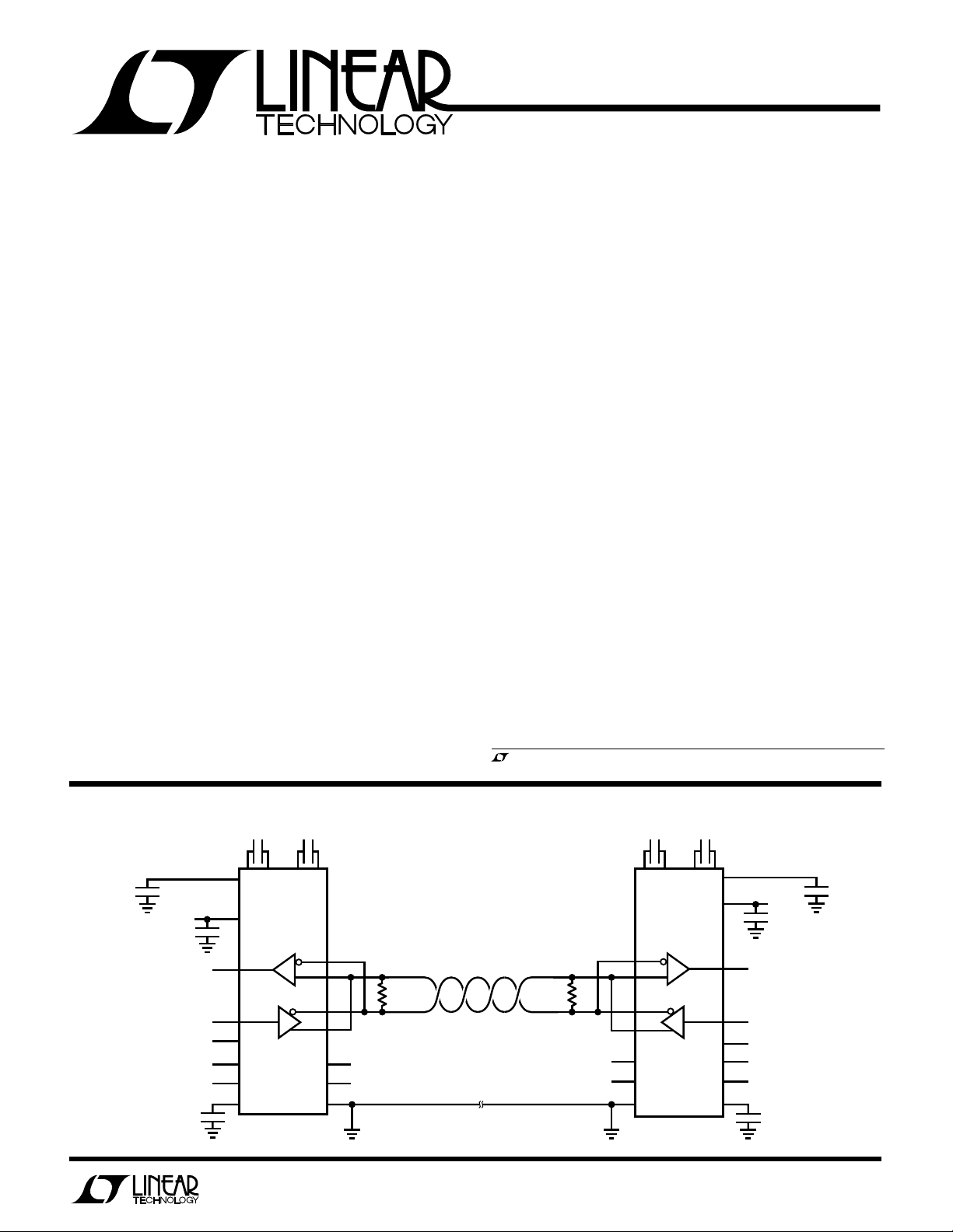
A
PPLICATITYPICAL
V
CC1
5V
RECOUT
DR IN
SLEW
DR ENABLE
U
O
12
3
LTC1387
18
17
15
14
9
12
5V
11
1920
4
5
6
7
8
13
10
120Ω
5V
5V
ALL CAPACITORS: 0.1µF MONOLITHIC CERAMIC TYPE
RS485 INTERFACE
4000-FT 24-GAUGE TWISTED PAIR
120Ω
LTC1387
4
5
6
7
8
5V
13
5V
10
212019
3
18
17
15
14
9
12
11
V
CC2
5V
RECOUT
DR IN
SLEW
DR ENABLE
5V
LTC1387 • TA01
1
Page 2
LTC1387
WU
U
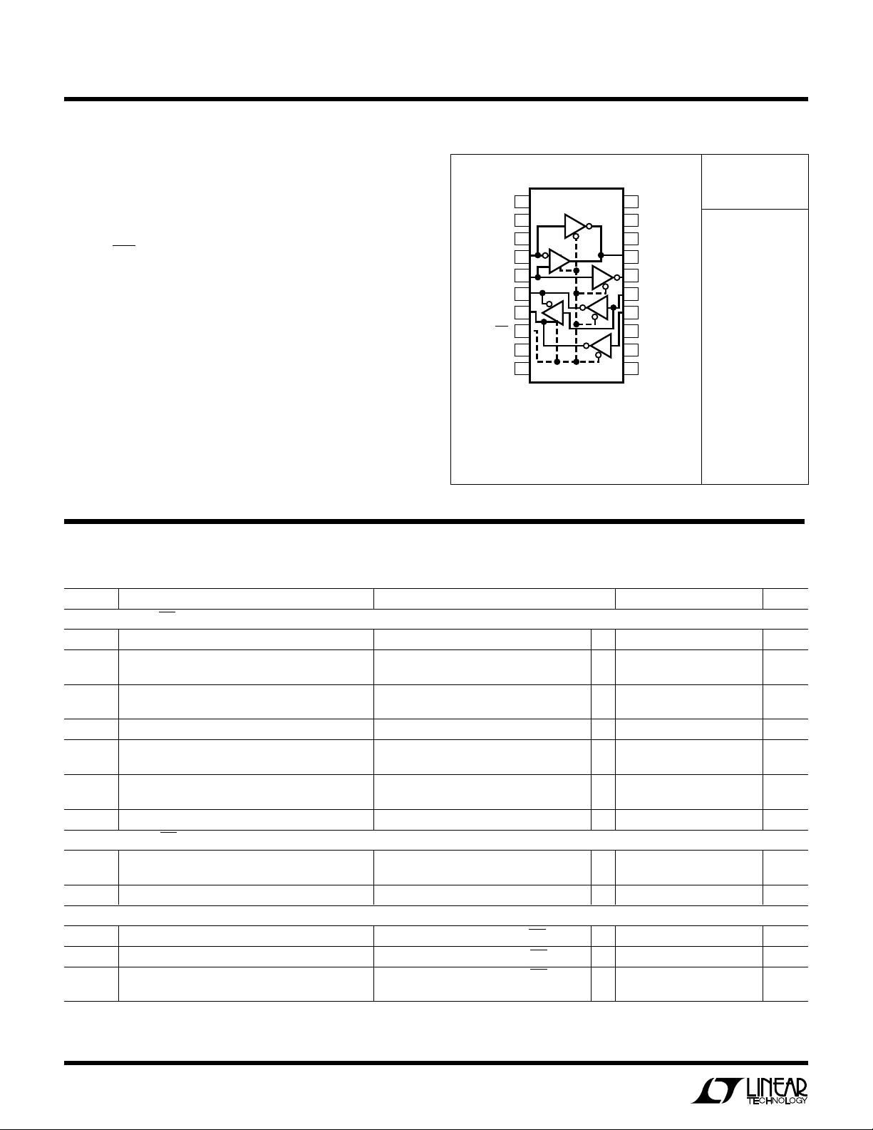
PACKAGE
/
O
RDER I FOR ATIO
A
W
O
LUTEXI T
S
A
WUW
ARB
U
G
I
S
(Note 1)
Supply Voltage (VCC) ............................................. 6.5V
Input Voltage
Drivers ................................... –0.3V to (VCC + 0.3V)
Receivers ............................................. –25V to 25V
485/232, ON, DXEN
RXEN, SLEW........................... –0.3V to (VCC + 0.3V)
Output Voltage
Drivers ................................................. –18V to 18V
Receivers ............................... –0.3V to (VCC + 0.3V)
Short-Circuit Duration
Output........................................................ Indefinite
VDD, VEE, C1+, C1–, C2+, C2–.......................... 30 sec
Operating Temperature Range
LTC1387C .............................................. 0°C to 70°C
LTC1387I ...........................................–40°C to 85°C
Storage Temperature Range................ –65°C to 150°C
Lead Temperature (Soldering, 10 sec)................ 300°C
TOP VIEW
+
1
C1
–
2
C1
3
V
DD
4
A
5
B
6
Y
7
Z
8
485/232
9
DXEN
10
GND
G PACKAGE
20-LEAD PLASTIC SSOP
T
= 125°C, θJA = 120°C/W (G)
JMAX
= 125°C, θJA = 75°C/W (SW)
T
JMAX
Consult factory for Military grade parts.
20
19
18
17
16
15
14
13
12
11
SW PACKAGE
20-LEAD PLASTIC SO
C2+
–
C2
V
CC
R
A
R
B
D
Y
DZ/SLEW
ON
RXEN
V
EE
ORDER PART
NUMBER
LTC1387CG
LTC1387CSW
LTC1387IG
LTC1387ISW
DC ELECTRICAL CHARACTERISTICS
TA = 25°C, VCC = 5V, C1 = C2 = C3 = C4 = 0.1µF (Notes 2, 3), unless otherwise noted.
SYMBOL PARAMETER CONDITIONS MIN TYP MAX UNITS
RS485 Driver (485/232 = High, ON = DXEN = High)
V
OD1
V
OD2
∆V
OD
V
OC
∆VOC Change in Magnitude of Driver Common Mode Figure 1, R = 27Ω or R = 50Ω ● 0.2 V
I
OSD
I
OZD
RS232 Driver (485/232 = Low, ON = DXEN = High)
V
O
I
OSD
Driver Inputs and Control Inputs
V
IH
V
IL
I
IN
Differential Driver Output Voltage (Unloaded) IO = 0 ● 6V
Differential Driver Output Voltage (With Load) Figure 1, R = 50Ω (RS422) ● 2.0 6 V
Figure 1, R = 27Ω (RS485) ● 1.5 6 V
Change in Magnitude of Driver Differential Figure 1, R = 27Ω or R = 50Ω ● 0.2 V
Output Voltage for Complementary Output States
Driver Common Mode Output Voltage Figure 1, R = 27Ω or R = 50Ω ● 3V
Output Voltage for Complementary Output States
Driver Short-Circuit Current VO = –7V, 12V; VO = High ● 35 250 mA
VO = –7V, 12V; VO = Low (Note 4) ● 10 250 mA
Three-State Output Current (Y, Z) –7V ≤ VO ≤ 12V ±5 500 µA
Output Voltage Swing Figure 4, RL = 3k, Positive ● 5 6.5 V
Figure 4, RL = 3k, Negative ● –5 –6.5 V
Output Short-Circuit Current VO = 0V ● ±17 ±60 mA
Input High Voltage DY, DZ, DXEN, RXEN, ON, 485/232, SLEW ● 2V
Input Low Voltage DY, DZ, DXEN, RXEN, ON, 485/232, SLEW ● 0.8 V
Input Current DY, DZ, DXEN, RXEN, ON, 485/232 ● ±0.1 ±10 µA
SLEW (Note 5)
● 5 15 µA
2
Page 3
L TC1387
DC ELECTRICAL CHARACTERISTICS
TA = 25°C, VCC = 5V, C1 = C2 = C3 = C4 = 0.1µF (Notes 2, 3), unless otherwise noted.
SYMBOL PARAMETER CONDITIONS MIN TYP MAX UNITS
RS485 Receiver (485/232 = High, ON = RXEN = High)
V
TH
∆V
TH
I
IN
R
IN
RS232 Receiver (485/232 = Low, ON = RXEN = High)
V
TH
∆V
TH
R
IN
Receiver Output (ON = RXEN = High)
V
OH
V
OL
I
OSR
I
OZR
Power Supply Generator
V
DD
V
EE
Power Supply
I
CC
Differential Input Threshold Voltage –7V ≤ VCM ≤ 12V ● –0.20 0.20 V
Input Hysteresis VCM = 0V 40 mV
Input Current (A, B) VIN = 12V ● 1mA
= –7V ● –0.8 mA
V
IN
Input Resistance –7V ≤ VIN ≤ 12V ● 12 24 kΩ
Receiver Input Voltage Threshold Input Low Threshold ● 0.8 V
Input High Threshold
● 2.4 V
Receiver Input Hysteresis 0.6 V
Receiver Input Resistance VIN = ±10V 3 5 7 kΩ
Receiver Output High Voltage IO = –3mA, VIN = 0V, 485/232 = Low ● 3.5 4.6 V
Receiver Output Low Voltage IO = 3mA, VIN = 3V, 485/232 = Low ● 0.2 0.4 V
Short-Circuit Current 0V ≤ VO ≤ V
CC
● 785mA
Three-State Output Current RXEN = 0V ● ±0.1 ±10 µA
VDD Output Voltage No Load, ON = DXEN = RXEN = High 8 V
= –5mA, ON = DXEN = RXEN = High 7 V
I
DD
VEE Output Voltage No Load, ON = DXEN = RXEN = High –7.7 V
= 5mA, ON = DXEN = RXEN = High –7.0 V
I
EE
VCC Supply Current No Load, ON = DXEN = RXEN = High ● 725mA
Shutdown, ON = DXEN = RXEN = 0V
● 5 100 µA
AC ELECTRICAL CHARACTERISTICS
TA = 25°C, VCC = 5V, C1 = C2 = C3 = C4 = 0.1µF (Notes 2, 3), unless otherwise noted.
SYMBOL PARAMETER CONDITIONS MIN TYP MAX UNITS
RS232 Mode (ON = DXEN = RXEN = High, 485/232 = Low)
SR Slew Rate Figure 4, RL = 3k, CL = 15pF ● 30 V/µ s
Figure 4, R
t
T
t
PLH
t
PHL
t
PLH
t
PHL
Transition Time Figure 4, RL = 3k, CL = 2500pF ● 0.22 1.9 3.1 µs
Driver Input to Output Figures 4, 10, RL = 3k, CL = 15pF ● 0.6 4 µs
Driver Input to Output Figures 4, 10, RL = 3k, CL = 15pF ● 0.6 4 µs
Receiver Input to Output Figures 5, 11 ● 0.3 6 µs
Receiver Input to Output Figures 5, 11 ● 0.4 6 µs
RS485 Mode (Fast Slew Rate, ON = DXEN = High, 485/232 = High, SLEW = High)
t
PLH
t
PHL
t
SKEW
t
, t
r
f
Driver Input to Output Figures 2, 7, RL = 54Ω, CL = 100pF ● 15 40 70 ns
Driver Input to Output Figures 2, 7, RL = 54Ω, CL = 100pF ● 15 40 70 ns
Driver Output to Output Figures 2, 7, RL = 54Ω, CL = 100pF ● 515 ns
Driver Rise or Fall Time Figures 2, 7, RL = 54Ω, CL = 100pF ● 31540 ns
= 3k, CL = 1000pF ● 4V/µs
L
3
Page 4
LTC1387
AC ELECTRICAL CHARACTERISTICS
TA = 25°C, VCC = 5V, C1 = C2 = C3 = C4 = 0.1µF (Notes 2, 3), unless otherwise noted.
SYMBOL PARAMETER CONDITIONS MIN TYP MAX UNITS
RS485 Mode (Fast Slew Rate, ON = DXEN = High, 485/232 = High, SLEW = High)
t
ZL
t
ZH
t
LZ
t
HZ
RS485 Mode (Slow Slew Rate, ON = DXEN = High, 485/232 = High, SLEW = Low)
t
PLH
t
PHL
t
SKEW
tr, t
f
t
ZL
t
ZH
t
LZ
t
HZ
RS485 Mode (ON = RXEN = High, 485/232 = High)
t
PLH
t
PHL
t
SKEW
Receiver Output Enable/Disable (ON = High)
t
ZL
t
ZH
t
LZ
t
HZ
The ● denotes specifications which apply over the full operating
temperature range.
Note 1: Absolute Maximum Ratings are those values beyond which the life
of the device may be impaired.
Note 2: All currents into device pins are positive; all currents out of device
pins are negative. All voltages are referenced to device ground unless
otherwise specified.
Driver Enable to Output Low Figures 3, 8, CL = 100pF, S1 Closed ● 50 90 ns
Driver Enable to Output High Figures 3, 8, CL = 100pF, S2 Closed ● 50 90 ns
Driver Disable from Low Figures 3, 8, CL = 15pF, S1 Closed ● 50 90 ns
Driver Disable from High Figures 3, 8, CL = 15pF, S2 Closed ● 60 90 ns
Driver Input to Output Figures 2, 7, RL = 54Ω, CL = 100pF ● 100 700 1500 ns
Driver Input to Output Figures 2, 7, RL = 54Ω, CL = 100pF ● 100 700 1500 ns
Driver Output to Output Figures 2, 7, RL = 54Ω, CL = 100pF ● 200 750 ns
Driver Rise or Fall Time Figures 2, 7, RL = 54Ω, CL = 100pF ● 150 300 1500 ns
Driver Enable to Output Low Figures 3, 8, CL = 100pF, S1 Closed ● 600 1500 ns
Driver Enable to Output High Figures 3, 8, CL = 100pF, S2 Closed ● 600 1500 ns
Driver Disable from Low Figures 3, 8, CL = 15pF, S1 Closed ● 100 200 ns
Driver Disable from High Figures 3, 8, CL = 15pF, S2 Closed ● 100 200 ns
Receiver Input to Output Figures 2, 9, RL = 54Ω, CL = 100pF ● 20 70 140 ns
Receiver Input to Output Figures 2, 9, RL = 54Ω, CL = 100pF ● 20 70 140 ns
Differential Receiver Skew, t
Receiver Enable to Output Low Figures 6, 12, CL = 15pF, S1 Closed ● 40 90 ns
Receiver Enable to Output High Figures 6, 12, CL = 15pF, S2 Closed ● 40 90 ns
Receiver Disable from Low Figures 6, 12, CL = 15pF, S1 Closed ● 40 90 ns
Receiver Disable from High Figures 6, 12, CL = 15pF, S2 Closed ● 40 90 ns
PLH
– t
Figures 2, 9, R
PHL
= 54Ω, CL = 100pF 10 ns
L
Note 3: All typicals are given at V
and TA = 25°C.
Note 4: Short-circuit current for RS485 driver output low state folds back
above V
Note 5: SLEW includes an internal pull-up in RS485 mode.
. Peak current occurs around VO = 3V.
CC
= 5V, C1 = C2 = C3 = C4 = 0.1µF
CC
UUU
PIN FUNCTION S
C1+ (Pin 1): Commutating Capacitor C1 Positive Terminal.
Requires an external 0.1µ F capacitor between Pins 1 and 2.
C1– (Pin 2): Commutating Capacitor C1 Negative Terminal.
VDD (Pin 3): Charge Pump Positive Supply Output.
Requires an external 0.1µF capacitor to ground.
A (Pin 4): Receiver Input A. Inverting input of RS232
receiver A in RS232 mode; inverting RS485 receiver input
in RS485 mode.
4
B (Pin 5): Receiver Input B. Inverting input of RS232
receiver B in RS232 mode; noninverting RS485 receiver
input in RS485 mode.
Y (Pin 6): Driver Output Y. Inverting RS232 driver Y output
in RS232 mode; inverting RS485 driver output in RS485
mode.
Z (Pin 7): Driver Output Z. Inverting RS232 driver Z output
in RS232 mode; noninverting RS485 driver output in
RS485 mode.
Page 5

L TC1387
U
UU
PI FU CTIO S
485/232 (Pin 8): Interface Mode Select Input. A low logic
input enables two RS232 drivers and two RS232 receivers. A high input enables the RS485 driver and the RS485
receiver.
DXEN (Pin 9): Driver Enable Input. A high logic input
enables the drivers and a low logic input disables the
drivers. When disabled, all driver outputs are in high
impedance
GND (Pin 10): Ground.
VEE (Pin 11): Charge Pump Negative Supply Output.
Requires an external 0.1µF capacitor to ground.
RXEN (Pin 12): Receiver Enable Input. A high logic input
enables the receivers and a low logic input disables the
receivers. When disabled, all receiver outputs are in high
impedance.
ON (Pin 13): A high logic level at ON input keeps the charge
pump active regardless of the state of the DXEN and RXEN
inputs. When the charge pump is active, the drivers and
receivers can be enabled or disabled without waiting for
charge pump stabilization time (typically 100µ s with 0.1µF
capacitors). A low logic state at the ON, DXEN and RXEN
inputs will put the transceiver and charge pump in shutdown mode and reduces ICC to 5µ A. Whenever the transceiver is activated from shutdown, the charge pump
should be allowed to stabilize before data transmission.
When DXEN and RXEN are high and ON is low, the charge
pump, drivers and receivers are all active and the driver
outputs are internally looped back to the inputs of the
receiver. The three control inputs ON, DXEN and RXEN can
be configured for one-, two- or three-wire control: onewire mode – all three inputs connected together; two-wire
mode – inputs ON and RXEN connected to one wire, DXEN
a separate wire; three-wire mode – separate wires to each
input. See the Function Tables.
DZ/SLEW (Pin 14): Driver Z or Slew Input. In RS232
mode, this pin is the driver Z input. In RS485 mode, this
pin controls the slew rate of the RS485 driver. With the
SLEW pin high, the RS485 driver runs at maximum (fast)
slew rate and can transmit signals up to 5MBd. With the
SLEW pin low, the RS485 driver runs with reduced (slow)
slew rate to control reflections with improperly terminated
cables. In slow mode, the RS485 driver can support data
rates up to 150kBd. This SLEW pin has internal 5µ A pullup during RS485 mode.
DY (Pin 15): Driver Y Input. Input Y in RS232 mode; the
differential driver input in RS485 mode.
RB (Pin 16): Receiver B Output. Output B in RS232 mode;
output is high impedance in RS485 mode.
RA (Pin 17): Receiver A Output. Output A in RS232 mode;
the differential receiver output in RS485 mode.
VCC (Pin 18): Positive Supply. 4.75V ≤ VCC ≤ 5.25V.
Requires an external 0.1µF bypass capacitor to ground.
–
C2
(Pin 19): Commutating Capacitor C2 Negative Termi-
nal. Requires an external 0.1µ F capacitor between Pins 19
and 20.
C2+ (Pin 20): Commutating Capacitor C2 Positive
Terminal.
5
Page 6

LTC1387
UU
FU CTIO TABLES
Select Modes
SELECT INPUTS RECEIVER DRIVER
ON RXEN DXEN 485/232 RXA RXB DXY DXZ
1 0 0 0 Z Z Z Z ON OFF RS232 Mode, DX and RX Off
1 0 1 0 Z Z ON ON ON OFF RS232 Mode, DXY and DXZ On, RX Off
1 1 0 0 ON ON Z Z ON OFF RS232 Mode, DX Off, RXA and RXB On
1 1 1 0 ON ON ON ON ON OFF RS232 Mode, DXY and DXZ On,
0 0 1 0 Z Z ON Z ON OFF RS232 Mode, DXY On, DXZ Off, RX Off
0 1 0 0 Z ON ON Z ON OFF RS232 Mode, DXY On,
0 1 1 0 ON ON ON ON ON ON RS232 Loopback Mode, DXY and DXZ On,
0 0 0 X Z Z Z Z OFF OFF Shutdown, RS485 R
1 0 0 1 Z Z Z Z ON OFF RS485 Mode, DX and RX Off
X 0 1 1 Z Z ON ON ON OFF RS485 Mode, DX On, RX Off
X 1 0 1 ON Z Z Z ON OFF RS485 Mode, DX Off, RX On
1 1 1 1 ON Z ON ON ON OFF RS485 Mode, DX On, RX On
0 1 1 1 ON Z ON ON ON ON RS485 Loopback Mode, DX On, RX On
CHARGE PUMP LOOPBACK COMMENTS
RXA and RXB On
DXZ Off, RXA Off, RXB On
RXA and RXB On
IN
RS232 Driver Mode
INPUTS
SELECTED 485/232 D CONDITIONS Y, Z
YES 0 0 No Fault 1
YES 0 1 No Fault 0
YES 0 X Thermal Fault Z
NO 0 X X Z
OUTPUTS
RS232 Receiver Mode
INPUTS
SELECTED 485/232 A, B R
YES 0 0 1
YES 0 1 0
YES 0 Inputs Open 1
NO 0 X Z
OUTPUTS
RS485 Driver Slew Rate
INPUTS
DXEN 485/232 SLEW SLEW RATE
1 1 0 Slow
1 1 1 Fast
01X Z
OUTPUTS
RS485 Driver Mode
INPUTS OUTPUTS
DXEN 485/232 D CONDITIONS Z Y
, R
A
B
1 1 0 No Fault 0 1
1 1 1 No Fault 1 0
1 1 X Thermal Fault Z Z
01XXZZ
RS485 Receiver Mode
INPUTS OUTPUTS
RXEN 485/232 B – A R
1 1 < –0.2V 0 Z
1 1 > 0.2V 1 Z
1 1 Inputs Open 1 Z
or Shorted to Ground
01 X ZZ
R
A
B
6
Page 7

BLOCK DIAGRAM
L TC1387
W
RS232 MODE
WITHOUT LOOPBACK
2
V
DD
485/232
3
4
A
5
B
6
Y
7
Z
8
9
DXEN
10
GND
*485/232, DXEN, RXEN = V
TEST CIRCUITS
Y
R
V
OD
V
OC
R
RS485 MODE
DXEN
GND
SLEW
2
3
4
A
5
B
6
Y
7
Z
8
9
10
D
WITHOUT LOOPBACK
Y
R
Z
201
C2C1
19
18
17
16
15
14
13
12
11
L
V
CC
R
A
R
B
D
Y
SLEW
ON
RXEN
V
EE
V
DD
485/232
DXEN*
GND
C
L
C
L
201
C2C1
19
18
17
16
15
14
13
12
11
CC
V
CC
R
A
R
B
D
Y
D
Z
ON
RXEN
V
EE
V
DD
485/232*
WITH LOOPBACK
2
3
6
Y
7
Z
8
9
10
A
B
RS232 MODE
R
15pF
RS485 MODE
DD
Y
Z
GND
DR OUT
WITH LOOPBACK
2
3
6
7
8
9
10
500Ω
C
L
V
CC
201
19
18
V
17
R
16
R
15
D
14
SLEW
13
12
11
LTC1387 • BD
S1
S2
CC
A
B
Y
ON
RXEN*
V
EE
C2C1
201
C2C1
19
18
V
17
R
16
R
15
D
14
D
13
12
11
CC
A
B
Y
Z
ON
RXEN*
V
EE
V
485/232*
DXEN*
Z
LTC1387 • F01
Figure 1. RS485 Driver
Test Load
Y, Z
D
C
L
232 = 0V, DXEN = 3V
Figure 4. RS232 Driver
Timing Test Circuit
R
L
LTC1387 • F04
485 = 3V, DXEN = 3V, RXEN = 3V
Figure 2. RS485 Driver/Receiver
Timing Test Circuit
Y, Z
D
232 = 0V, DXEN = 3V, RXEN = 3V
A, B
R
Figure 5. RS232 Receiver
Timing Test Circuit
LTC1387 • F02
15pF
LTC1387 • F05
LTC1387 • F03
Figure 3. RS485 Driver Output
Enable/Disable Timing Test Load
V
CC
S1
C
1k
L
S2
LTC1387 • F06
RECEIVER
OUT
Figure 6. Receiver Output
Enable/Disable Timing Test Load
7
Page 8

LTC1387
U
W
SWITCHI G WAVEFOR S
f = 1MHz: t
f = 100kHz: t
3V
1.5V
t
PLH
50%
10%
O
Figure 7. RS485 Driver Propagation Delays
f = 1MHz: t
f = 100kHz: t
1.5V
t
ZL
t
ZH
Figure 8. RS485 Driver Enable and Disable Times
Z – Y
DXEN
Y, Z
Z, Y
D
0V
V
O
–V
O
Y
V
Z
3V
0V
5V
V
OL
V
OH
0V
≤ 10ns: tf ≤ 10ns (FAST SLEW RATE MODE)
r
≤ 10ns: tf ≤ 10ns (SLOW SLEW RATE MODE)
r
90%
t
r
t
SKEW
≤ 10ns: tf ≤ 10ns (FAST SLEW RATE MODE)
r
≤ 10ns: tf ≤ 10ns (SLOW SLEW RATE MODE)
r
2.3V
2.3V
V
= V(A) – V(B)
DIFF
1/2 V
O
OUTPUT NORMALLY LOW
OUTPUT NORMALLY HIGH
1.5V
1.5V
t
PHL
90%
t
LZ
t
HZ
50%
10%
t
f
t
LTC1387 • F07
SKEW
0.5V
0.5V
LTC1387 • F08
8
B – A
–V
R
Y, Z
V
V
OD2
OD2
V
f = 1MHz: t
0V
t
PLH
OH
OL
≤ 10ns: tf ≤ 10ns
r
1.5V
INPUT
OUTPUT
0V
t
PHL
1.5V
LTC1387 • F09
Figure 9. RS485 Receiver Propagation Delays
3V
D
0V
V
O
–V
O
1.5V
t
PHL
0V
1.5V
t
PLH
0V
LTC1387 • F10
Figure 10. RS232 Driver Propagation Delays
Page 9

L TC1387
U
W
SWITCHI G WAVEFOR S
V
IH
A, B
R
RXEN
V
IL
V
OH
V
OL
3V
0V
5V
R
V
OL
V
OH
R
0V
1.3V
Figure 11. RS232 Receiver Propagation Delays
1.5V
Figure 12. Receiver Enable and Disable Times
t
t
t
PHL
ZL
ZH
0.8V
f = 1MHz: t
1.5V
1.5V
≤ 10ns: tf ≤ 10ns
r
OUTPUT NORMALLY LOW
OUTPUT NORMALLY HIGH
1.7V
1.5V
t
t
HZ
t
PLH
2.4V
LZ
0.5V
0.5V
LTC1387 • F11
LTC1387 • F12
PPLICATI
A
U
O
S
I FOR ATIO
WU
U
Basic Theory of Operating
The LTC1387 is a single 5V supply, single-port logic
reconfigurable RS485/RS232 transceiver with an onboard
charge pump. The interface port offers a flexible combination of an RS485 driver and an RS485 receiver or two
RS232 drivers and two RS232 receivers. The RS485
transceiver and the RS232 transceivers are designed to
share the same I/O pins. A logic input 485/232 controls the
selection between RS485 and RS232 transceiver modes.
The RS485 transceiver supports both RS485 and RS422
standards, whereas the RS232 transceivers support both
RS232 and EIA562 standards. With four additional control
inputs: ON, DXEN, RXEN and SLEW, the LTC1387 can
easily be reconfigured via software to adapt to various
communication needs including a one-signal-line RS232
I/O mode. Four examples of interface port connections are
shown in Figures 13 through 16.
Both the interface drivers and the receivers feature threestate outputs. Driver outputs are forced into high
impedance when the driver is disabled, in the shutdown
mode or with the power off. The driver outputs can be
forced beyond power supply levels without damage up to
±18V. The receiver inputs can withstand ±25V without
damage. The receiver input resistance is typically 24k in
RS485 mode, shutdown mode or power off but drops to
5k in RS232 mode.
In RS485 mode, the DXEN and RXEN control the threestate outputs of the driver and receiver respectively. The
SLEW input is active during RS485 mode and the logic
level controls the differential driver slew rate. This pin has
an internal 5µA pull-up current source during the RS485
mode. A high logic selects fast differential driver slew rate
and a low logic selects slow slew rate. In slow slew mode,
the maximum signal bandwidth is reduced, minimizing
9
Page 10

LTC1387
PPLICATI
A
U
O
S
I FOR ATIO
WU
U
EMI and signal reflection problems. Slow slew rate systems can often use improperly terminated or even
unterminated cables with acceptable results. The RS485
differential input receiver features an offset input threshold of –80mV at 0V common mode voltage. This allows
the receiver output to have a known High output state
when the inputs are open or shorted. The receiver also
features an input hysteresis of 40mV. The charge pump
can be kept active regardless of the state of DXEN and
RXEN pins by keeping the ON pin High. This improves the
receiver response time by removing the 100µs charge
pump start-up time.
In RS232 mode, the drivers and receivers can be selected
from the Function Tables with control inputs ON, RXEN
and DXEN. The receivers feature a typical 0.6V input
hysteresis.
All the interface driver outputs are fault protected by a
current limiting and thermal shutdown circuit. The thermal
shutdown circuit disables both the RS232 and RS485
driver outputs when the die temperature reaches 150°C.
The thermal shutdown circuit reenables the drivers when
the die temperature cools to 135°C.
A loopback mode enables internal connections from driver
outputs to receiver inputs for self-test. The driver outputs
are not isolated from the external loads during loopback.
The charge pump generates boosted positive voltage V
DD
and negative voltage VEE for true RS232 levels from a
single 5V VCC supply. The charge pump requires four
0.1µF capacitors.
RS232 RS485
A
INTERFACE
B
RS232 RS232 RS485 RS485 SHUTDOWN
TRANSMIT MODE RECEIVE MODE TRANSMIT MODE RECEIVE MODE MODE
RXEN = 0 RXEN = 1 RXEN = 0 RXEN = 1 RXEN = 0
DXEN = 1 DXEN = 0 DXEN = 1 DXEN = 0 DXEN = 0
MODE = 0 MODE = 0 MODE = 1 MODE = 1 MODE = X
Figure 13. Half-Duplex RS232 (1-Channel), Half-Duplex RS485
RS485
LTC1387
R
A
B
D
Y
Z
D
A
R
A
R
B
R
B
Y
D
Y
DZ/SLEW
Z
ON
RXEN
DXEN
485/232
V
CC
DX/RX
CONTROLLER
RXEN
DXEN
MODE
1387 • F13
10
Page 11

L TC1387
R
A
R
B
D
Y
D
Z
A
B
Y
Z
R
A
R
B
D
Y
DZ/SLEW
ON
V
CC
RXEN
DXEN
485/232
CONTROLLER
DX
RXEN
DXEN
MODE
INTERFACE
A
B
RS232
RS232
RS485
RS485
RS232 RS485 RS485 SHUTDOWN
MODE TRANSMIT MODE RECEIVE MODE MODE
RXEN = 1 RXEN = 0 RXEN = 1 RXEN = 0
DXEN = 0 DXEN = 1 DXEN = 0 DXEN = 0
MODE = 0 MODE = 1 MODE = 1 MODE = 0
1387 • F14
LTC1387
RX
TXD
RXD
PPLICATI
A
INTERFACE
O
RS232
A
RXD
B
RS232 RS485
Y
TXD
Z
U
S
I FOR ATIO
Figure 14. Full-Duplex RS232 (1-Channel), Half-Duplex RS485
RS485
RS485
RS485
LTC1387
A
B
D
Y
Y
Z
D
Z
WU
R
R
A
B
U
R
A
R
B
D
Y
DZ/SLEW
ON
RXEN
DXEN
485/232
V
CC
RX
CONTROLLER
DX
RXEN
DXEN
MODE
RS232 RS485 SHUTDOWN
MODE MODE MODE
RXEN = 1 RXEN = 1 RXEN = 0
DXEN = 1 DXEN = 1 DXEN = 0
MODE = 0 MODE = 1 MODE = X
1387 • F15
Figure 15. Full-Duplex RS232 (1-Channel), Full-Duplex RS485/RS422
RS232
A
B
INTERFACE
Y
Z
RS485
RXD
RS232
RS485
CTS
RS232 RS485
TXD
RS232
RS485
RTS
Figure 16. Full-Duplex RS232 (2-Channel), Full-Duplex RS485/RS422 with SLEW Control
LTC1387
R
Y
Z
A
R
A
R
B
R
B
D
Y
DZ/SLEW
ON
RXEN
DXEN
485/232
RX1
RX2
CONTROLLER
DX1
DX2/SLEW
ON
RXEN
DXEN
MODE
RS232 RS485 SHUTDOWN
MODE MODE MODE
ON = 1 ON = 1 ON = 0
RXEN = 1 RXEN = 1 RXEN = 0
DXEN = 1 DXEN = 1 DXEN = 0
MODE = 0 MODE = 1 MODE = X
A
B
D
Y
Z
D
Information furnished by Linear Technology Corporation is believed to be accurate and reliable.
However, no responsibility is assumed for its use. Linear Technology Corporation makes no representation that the interconnection of its circuits as described herein will not infringe on existing patent rights.
1387 • F16
11
Page 12

LTC1387
PACKAGE DESCRIPTION
0.205 – 0.212**
(5.20 – 5.38)
U
Dimensions in inches (millimeters) unless otherwise noted.
G Package
20-Lead Plastic SSOP (0.209)
(LTC DWG # 05-08-1640)
0.278 – 0.289*
(7.07 – 7.33)
1718 14 13 12 1115161920
0.068 – 0.078
(1.73 – 1.99)
0° – 8°
0.005 – 0.009
(0.13 – 0.22)
*
DIMENSIONS DO NOT INCLUDE MOLD FLASH. MOLD FLASH
SHALL NOT EXCEED 0.006" (0.152mm) PER SIDE
**
DIMENSIONS DO NOT INCLUDE INTERLEAD FLASH. INTERLEAD
FLASH SHALL NOT EXCEED 0.010" (0.254mm) PER SIDE
0.022 – 0.037
(0.55 – 0.95)
0.0256
(0.65)
BSC
0.010 – 0.015
(0.25 – 0.38)
0.002 – 0.008
(0.05 – 0.21)
SW Package
20-Lead Plastic Small Outline (Wide 0.300)
(LTC DWG # 05-08-1620)
0.291 – 0.299**
(7.391 – 7.595)
0.010 – 0.029
(0.254 – 0.737)
0.009 – 0.013
(0.229 – 0.330)
NOTE:
1. PIN 1 IDENT, NOTCH ON TOP AND CAVITIES ON THE BOTTOM OF PACKAGES ARE THE MANUFACTURING OPTIONS.
THE PART MAY BE SUPPLIED WITH OR WITHOUT ANY OF THE OPTIONS
DIMENSION DOES NOT INCLUDE MOLD FLASH. MOLD FLASH SHALL NOT EXCEED 0.006" (0.152mm) PER SIDE
*
DIMENSION DOES NOT INCLUDE INTERLEAD FLASH. INTERLEAD FLASH SHALL NOT EXCEED 0.010" (0.254mm) PER SIDE
**
NOTE 1
× 45°
0.016 – 0.050
(0.406 – 1.270)
0.093 – 0.104
(2.362 – 2.642)
0° – 8° TYP
0.050
(1.270)
TYP
0.014 – 0.019
(0.356 – 0.482)
TYP
0.037 – 0.045
(0.940 – 1.143)
NOTE 1
0.004 – 0.012
(0.102 – 0.305)
12345678910
0.496 – 0.512*
(12.598 – 13.005)
19 181716
20
2345678
1
14 13
15
0.301 – 0.311
(7.65 – 7.90)
G20 SSOP 0595
1112
910
0.394 – 0.419
(10.007 – 10.643)
S20 (WIDE) 0396
RELATED PARTS
PART NUMBER DESCRIPTION COMMENTS
LTC485 Low Power RS485 Interface Transceiver Single 5V Supply, Wide Common Mode Range
LT®1137A Low Power RS232 Transceiver ±15kV IEC-1000-4-2 ESD Protection, Three Drivers, Five Receivers
LTC1320 AppleTalk® Transceiver AppleTalk/LocalTalk® Compliant
LTC1321/LTC1322/LTC1335 RS232/EIA562/RS485 Transceivers Configurable
LTC1323 Single 5V AppleTalk Transceiver AppleTalk /LocalTalk Compliant 10kV ESD
LTC1334 Single Supply RS232/RS485 Transceiver Single 5V Supply, Configurable
LTC1347 5V Low Power RS232 Transceiver Three Drivers/Five Receivers, Five Receivers Alive in Shutdown
AppleTalk and LocalTalk are registered trademarks of Apple Computer Corp.
1387f LT/GP 0197 7K • PRINTED IN USA
LINEAR TECHNOLOGY CORPORATION 1997
12
Linear Technology Corporation
1630 McCarthy Blvd., Milpitas, CA 95035-741 7 ● (408) 432-1900
FAX: (408) 434-0507
●
TELEX: 499-3977 ● www.linear-tech.com
 Loading...