

Page 1
FEATURES
■
Single Chip Provides All V.35 Differential Clock
and Data Signals
■
Operates From Single 5V Supply
■
Software Selectable DTE or DCE Configuration
■
Transmitters and Receivers Will Withstand
Repeated ±10kV ESD Pulses
■
Shutdown Mode Reduces ICC to 1µA Typ
■
10MBaud Transmission Rate
■
Transmitter Maintains High Impedance When
Disabled, Shut Down, or with Power Off
■
Meets CCITT V.35 Specification
■
Transmitters are Short-Circuit Protected
LTC1345
Single Supply
V.35 Transceiver
U
DESCRIPTIO
The LTC®1345 is a single chip transceiver that provides the
differential clock and data signals for a V.35 interface from
a single 5V supply. Combined with an external resistor
termination network and an LT®1134A RS232 transceiver
for the control signals, the LTC1345 forms a complete low
power DTE or DCE V.35 interface port operating from a
single 5V supply.
The LTC1345 features three current output differential
transmitters, three differential receivers, and a charge
pump. The transceiver can be configured for DTE or DCE
operation or shut down using two Select pins. In the
Shutdown mode, the supply current is reduced to 1µA.
U
APPLICATIO S
■
Modems
■
Telecommunications
■
Data Routers
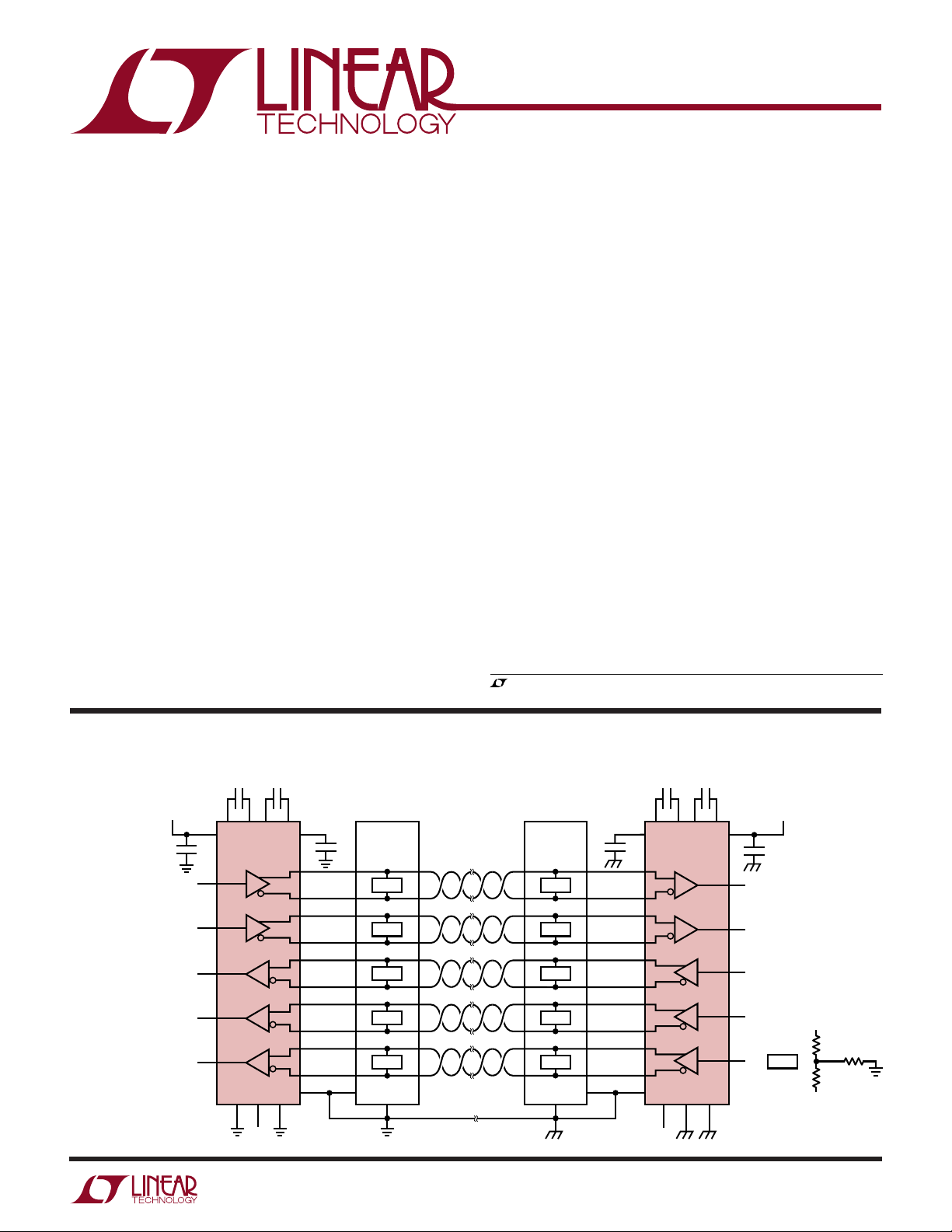
TYPICAL APPLICATIO
1µF
1µF 1µF1µF
V
CC1
5V
1µF
11
12
13
2
4
1
LTC1345 LTC1345
6
DX
7
DX
RX
RX
RX
10
14
9
V
CC1
The transceiver operates up to 10Mbaud. All transmitters
feature short-circuit protection and a Receiver Output
Enable pin allows the receiver outputs to be forced into a
high impedance state. Both transmitter outputs and receiver inputs feature ±10kV ESD protection. The charge
pump features a regulated VEE output using three external
1µF capacitors.
, LTC and LT are registered trademarks of Linear Technology Corporation.
U
Clock and Data Signals for V.35 Interface
DCEDTE
28
273
26
25
24
23
20
19
18
17
16
15
5
1µF
1
2
3
4
14
13
12
11
10
9
7
BI
627T500/1250
T
T T
T T
T T
T T
8
TXD (103)
SCTE (113)
TXC (114)
RXC (115)
RXD (104)
GND (102)
BI
627T500/1250
T
8
12
111817
10
9
1
2
3
4
5
6
7
1µF
16
15
26
25
24
23
22
21
1
28
2
4
RX
RX
DX
DX
DX
5
10 14
9
V
CC2
V
327
1µF
12
13
6
7
8
627T500/1250 (SOIC) OR
LTC1345 • TA01
CC2
5V
50Ω
=
T
50Ω
BI TECHNOLOGIES
899TR50/125 (DIP)
125Ω
1
Page 2
LTC1345
PACKAGE/ORDER I FOR ATIO
UU
W
WWWU
ABSOLUTE AXI U RATI GS
(Note 1)
Supply Voltage, VCC.................................................. 6V
Input Voltage
Transmitters ........................... –0.3V to (VCC + 0.3V)
Receivers............................................... –18V to 18V
S1, S2, OE ............................... –0.3V to (VCC + 0.3V)
Output Voltage
Transmitters .......................................... –18V to 18V
Receivers................................ –0.3V to (VCC + 0.3V)
VEE........................................................ –10V to 0.3V
Short-Circuit Duration
Transmitter Output ..................................... Indefinite
Receiver Output.......................................... Indefinite
VEE................................................................. 30 sec
Operating Temperature Range
Commercial ............................................ 0°C to 70°C
Industrial ........................................... – 40°C to 85°C
Storage Temperature Range ................ – 65°C to 150°C
Lead Temperature (Soldering, 10 sec)................. 300°C
TOP VIEW
+
1
C2
+
2
C1
3
V
CC
–
4
C1
5
GND
6
T1
7
T2
8
T3
9
S1
10
S2
11
R3
12
R2
13
R1
14
OE
NW PACKAGE
28-LEAD PDIP
THREE V.35 TRANSMITTERS AND THREE RECEIVERS
T
= 125°C, θ
JMAX
T
= 125°C, θ
JMAX
SW PACKAGE
28-LEAD PLASTIC SO
= 56°C/W (NW)
JA
= 65°C/W (SW)
JA
–
28
C2
27
V
EE
26
Y1
25
Z1
24
Y2
23
Z2
22
Y3
21
Z3
20
B3
19
A3
18
B2
17
A2
16
B1
15
A1
ORDER PART
NUMBER
LTC1345CNW
LTC1345CSW
LTC1345INW
LTC1345ISW
Consult factory for Military grade parts.
DC ELECTRICAL CHARACTERISTICS
The ● denotes specifications which apply over the full operating
temperature range, otherwise specifications are at TA = 25°C. VCC = 5V ±5% (Notes 2, 3), unless otherwise specified.
SYMBOL PARAMETER CONDITIONS MIN TYP MAX UNITS
V
V
I
OH
I
OL
I
OZ
R
V
∆V
I
IN
R
V
V
I
OSR
I
OZR
V
V
I
IN
I
CC
V
OD
OC
O
TH
TH
IN
OH
OL
IH
IL
EE
Transmitter Differential Output Voltage Figure 1, –4V ≤ VOS ≤ 4V ● 0.44 0.55 0.66 V
Transmitter Common-Mode Output Voltage Figure 1, VOS = 0V ● –0.6 0 0.6 V
Transmitter Output High Current V
Transmitter Output Low Current V
Transmitter Output Leakage Current S1 = S2 = 0V, –5V ≤ V
Transmitter Output Impedance –2V ≤ V
= 0V ● –12.6 –11 – 9.4 mA
Y, Z
= 0V ● 9.4 11 12.6 mA
Y, Z
≤ 5V ● ±1 ±100 µA
Y, Z
≤ 2V 100 kΩ
Y, Z
Differential Receiver Input Threshold Voltage –7V ≤ (VA + VB)/2 ≤ 7V ● 25 200 mV
Receiver Input Hysterisis –7V ≤ (VA + VB)/2 ≤ 7V 50 mV
Receiver Input Current (A, B) –7V ≤ V
Receiver Input Impedance –7V ≤ V
Receiver Output High Voltage IO = 4mA, V
Receiver Output Low Voltage IO = 4mA, V
Receiver Output Short-Circuit Current 0V ≤ VO ≤ V
Receiver Three-State Output Current S1 = S2 = 0V, 0V ≤ VO ≤ V
≤ 7V ● 0.4 mA
A, B
≤ 7V ● 17.5 30 kΩ
A, B
= 0.2V ● 3 4.5 V
B, A
= –0.2V ● 0.2 0.4 V
B, A
CC
CC
● 785mA
● ±10 µA
Logic Input High Voltage T, S1, S2, OE ● 2V
Logic Input Low Voltage T, S1, S2, OE ● 0.8 V
Logic Input Current T, S1, S2, OE ● ±10 µA
VCC Supply Current Figure 1, VOS = 0, S1 = S2 = HIGH ● 118 170 mA
No Load, S1 = S2 = HIGH
Shutdown, S1 = S2 = 0V
● 19 30 mA
● 1 100 µA
VEE Voltage No Load, S1 = S2 = HIGH –5.5 V
2
Page 3
LTC1345
TEMPERATURE (˚C)
–50
TIME (ns)
25
LTC1345 • TPC03
10
5
–25 0 50
0
20
15
75 100 125
VCC = 5V
AC ELECTRICAL CHARACTERISTICS
The ● denotes specifications which apply over the full operating
temperature range, otherwise specifications are at TA = 25°C. VCC = 5V ±5% (Notes 2, 3), unless otherwise specified.
SYMBOL PARAMETER CONDITIONS MIN TYP MAX UNITS
tR, t
F
t
PLH
t
PHL
t
SKEW
t
PLH
t
PHL
t
SKEW
t
ZL
t
ZH
t
LZ
t
HZ
f
OSC
BR
MAX
Note 1: The absolute maximum ratings are those values beyond which the
safety of the device cannot be guaranteed.
Note 2: All currents into device pins are termed positive; all currents out of
device pins are termed negative. All voltages are referenced to device
ground unless otherwise specified.
Transmitter Rise or Fall Time Figures 1 and 3, VOS = 0V ● 740 ns
Transmitter Input to Output Figures 1 and 3, VOS = 0V ● 25 70 ns
Transmitter Input to Output Figures 1 and 3, VOS = 0V ● 25 70 ns
Transmitter Output to Output Figures 1 and 3, VOS = 0V 0 ns
Receiver Input to Output Figures 1 and 4, VOS = 0V ● 49 100 ns
Receiver Input to Output Figures 1 and 4, VOS = 0V ● 52 100 ns
Differential Receiver Skew, t
PLH
– t
PHL
Figures 1 and 4, VOS = 0V 3 ns
Receiver Enable to Output LOW Figures 2 and 5, CL = 15pF, S1 Closed ● 40 70 ns
Receiver Enable to Output HIGH Figures 2 and 5, CL = 15pF, S2 Closed ● 35 70 ns
Receiver Disable From LOW Figures 2 and 5, CL = 15pF, S1 Closed ● 30 70 ns
Receiver Disable From HIGH Figures 2 and 5, CL = 15pF, S2 Closed ● 35 70 ns
Charge Pump Oscillator Frequency 200 kHz
Maximum Data Rate (Note 4) ● 10 15 Mbaud
Note 3: All typicals are given for VCC = 5V, C1 = C2 = C3 = 1µF ceramic
capacitors and T
= 25°C.
A
Note 4: Maximum data rate is specified for NRZ data encoding scheme.
The maximum data rate may be different for other data encoding schemes.
Data rate is guaranteed by correlation and is not tested.
UW
TYPICAL PERFOR A CE CHARACTERISTICS
Transmitter Output Current
vs Output Voltage
13
TA = 25°C
= 5V
V
CC
12
11
10
OUTPUT CURRENT (mA)
9
–1.5
–2.0
–0.5
–1.0
OUTPUT VOLTAGE (V)
OUTPUT CURRENT (mA)
Transmitter Output Current
vs Temperature
13
VCC = 5V
12
11
10
9
–25 0 50
–50
25
TEMPERATURE (˚C)
75 100 125
LTC1345 • TPC01
Transmitter Output Skew
vs Temperature
0.5
0
1.0
1.5
LTC1345 • TPC02
2.0
3
Page 4
LTC1345
TEMPERATURE (˚C)
–50
VOLTAGE (V)
25
LTC1345 • TPC06
–5.5
–6.0
–25 0 50
–6.5
–4.5
–5.0
75 100 125
VCC = 5V
UW
TYPICAL PERFOR A CE CHARACTERISTICS
Receiver t
vs Temperature
20
VCC = 5V
15
10
TIME (ns)
5
0
–25 0 50
–50
– t
PLH
TEMPERATURE (˚C)
PHL
25
75 100 125
LTC1345 • TPC04
Transmitter Output Waveforms
INPUT
5V/DIV
OUTPUT
0.2V/DIV
Supply Current vs Temperature
140
VCC = 5V
120
100
CURRENT (mA)
80
60
–25 0 50
–50
LOADED
NO LOAD
25
TEMPERATURE (˚C)
30
25
CURRENT (mA)
20
15
75 100 125
LTC1345 • TPC05
10
Receiver Output Waveforms
INPUT
0.2/DIV
OUTPUT
5V/DIV
VEE Voltage vs Temperature
LTC1345 • TPC07
U
UU
PI FU CTIO S
C2+ (Pin 1):
C1+ (Pin 2): Capacitor C1 Positive Terminal.
VCC (Pin 3): Positive Supply, 4.75 ≤ VCC ≤ 5.25V.
C1– (Pin 4): Capacitor C1 Negative Terminal.
GND (Pin 5): Ground. The positive terminal of C3 is
connected to ground.
T1 (Pin 6): Transmitter 1 Input.
T2 (Pin 7): Transmitter 2 Input.
T3 (Pin 8): Transmitter 3 Input.
S1 (Pin 9): Select Input 1.
S2 (Pin 10): Select Input 2.
Capacitor C2 Positive Terminal.
LTC1345 • TPC08
R3 (Pin 11): Receiver 3 Output.
R2 (Pin 12): Receiver 2 Output.
R1 (Pin 13): Receiver 1 Output.
OE (Pin 14): Receiver Output Enable.
A1 (Pin 15): Receiver 1 Inverting Input.
B1 (Pin 16): Receiver 1 Noninverting Input.
A2 (Pin 17): Receiver 2 Inverting Input.
B2 (Pin 18): Receiver 2 Noninverting Input.
A3 (Pin 19): Receiver 3 Inverting Input.
B3 (Pin 20): Receiver 3 Noninverting Input.
Z3 (Pin 21): Transmitter 3 Inverting Output.
4
Page 5

LTC1345
U
UU
PI FU CTIO S
Y3 (Pin 22): Transmitter 3 Noninverting Output.
Z2 (Pin 23): Transmitter 2 Inverting Output.
Y2 (Pin 24): Transmitter 2 Noninverting Output
Z1 (Pin 25): Transmitter 1 Inverting Output.
U
U
FU CTIO TABLES
Transmitter and Receiver Configuration
S1 S2 TX# RX# REMARKS
0 0 — — Shutdown
1 0 1, 2, 3 1, 2 DCE Mode, RX3 Shut Down
0 1 1, 2 1, 2, 3 DTE Mode, TX3 Shut Down
1 1 1, 2, 3 1, 2, 3 All Active
Transmitter
INPUTS OUTPUTS
CONFIGURATION S1 S2 T Y1 AND Y2 Z1 AND Z2 Y3 Z3
DTE 0 1 0 0 1 Z Z
DTE 0 1 1 1 0 Z Z
DCE or All ON 1 X 0 0 1 0 1
DCE or All ON 1 X 1 1 0 1 0
Shutdown 0 0 X Z Z Z Z
Y1 (Pin 26): Transmitter 1 Noninverting Output.
VEE (Pin 27): Charge Pump Output. Connected to negative
terminal of capacitor C3.
C2– (Pin 28): Capacitor C2 Negative Terminal.
Receiver
INPUTS OUTPUTS
CONFIGURATION S1 S2 OE B – A R1 AND R2 R3
DTE or All ON X 1 0 ≥0.2V 1 1
DTE or All ON X 1 0 ≤–0.2V 0 0
DCE 1 0 0 ≥0.2V 1 Z
DCE 1 0 0 ≤–0.2V 0 Z
Disabled X X 1 X Z Z
Shutdown 0 0 X X Z Z
TEST CIRCUITS
Y
Y
T
Z
Figure 1. V.35 Transmitter/Receiver Test Circuit
50Ω
125Ω
V
OD
50Ω
VOC = (VY + VZ)/2
Z
V
CC
S1
S2
LTC1345 • F02
125Ω
50Ω
50Ω
B
R
A
15pFOE
LTC1345 • F01
RECEIVER
OUTPUT
V
OS
1k
C
L
Figure 2. Receiver Output Enable/Disable Timing Test Load
5
Page 6

LTC1345
UWW
SWITCHI G TI E WAVEFOR S
Y – Z
B – A
3V
T
0V
V
O
–V
O
Z
V
Y
O
1.5V
10%
f = 1MHz: t
t
PLH
50%
t
r
≤ 10ns: tf ≤ 10ns
r
90%
t
SKEW
V
1/2 V
DIFF
= V(Y) – V(Z)
O
1.5V
t
PHL
90%
50%
10%
t
f
t
LTC1345 • F03
SKEW
Figure 3. V.35 Transmitter Propagation Delays
V
ID
–V
ID
V
OH
R
V
OL
0V
t
PLH
f = 1MHz: t
≤ 10ns: tf ≤ 10ns
r
1.5V
INPUT
OUTPUT
0V
t
PHL
1.5V
LTC1345 • F04
Figure 4. V.35 Receiver Propagation Delays
3V
OE
0V
5V
R
V
OL
V
OH
R
0V
1.5V
f = 1MHz: t
t
ZL
1.5V
t
ZH
1.5V
≤ 10ns: tf ≤ 10ns
r
OUTPUT NORMALLY LOW
OUTPUT NORMALLY HIGH
1.5V
t
t
HZ
LZ
0.5V
0.5V
LTC1345 • F05
Figure 5. Receiver Enable and Disable Times
6
Page 7

WUUU
APPLICATIO S I FOR ATIO
LTC1345
Review of CCITT Recommendation V.35
Electrical Specifications
V.35 is a CCITT recommendation for synchronous data
transmission via modems. Appendix 2 of the recommendation describes the electrical specifications which are
summarized below:
1. The interface cable is balanced twisted-pair with 80Ω to
120Ω impedance.
2. The transmitter’s source impedance is between 50Ω and
150Ω.
3. The transmitter’s resistance between shorted terminals
and ground is 150Ω ±15Ω.
4. When terminated by a 100Ω resistive load, the terminalto-terminal voltage should be 0.55V ±20%.
5. The transmitter’s rise time should be less than 1% of the
signal pulse or 40ns, whichever is greater.
6. The common-mode voltage at the transmitter output
should not exceed 0.6V.
Cable Termination
Each end of the cable connected to an LTC1345 must be
terminated by either one of two electrically equivalent
external Y or ∆ resistor networks for proper operation. The
Y-termination has two series connected 50Ω resistors and
a 125Ω resistor connected between ground and the center
tap of the two 50Ω resistors as shown in Figure 6A.
50Ω
125Ω
50Ω
A
300Ω
120Ω
300Ω
B
Figure 6. Y and ∆ Termination Networks
LTC1345 • F06
7. The receiver impedance is 100Ω ±10Ω.
8. The receiver impedance to ground is 150Ω ±15Ω.
9. The transmitter or receiver should not be damaged by
connection to earth ground, short-circuiting, or cross
connection to other lines.
10. No data errors should occur with ±2V common-mode
change at either the transmitter or receiver, or ±4V ground
potential difference between transmitter and receiver.
The alternative ∆-termination has a 120Ω resistor across
the twisted wires and two 300Ω resistors between each
wire and ground as shown in Figure 6B. Standard 1/8W,
5% surface mount resistors can be used for the termination
network. To maintain the proper differential output swing,
the resistor tolerance must be 5% or less. A termination
network that combines all the resistors into an SO-14
package is available from:
BI Technologies (Formerly Beckman Industrial)
Resistor Networks
4200 Bonita Place
Fullerton, CA 92635
Phone: (714) 447-2357
FAX: (714) 447-2500
Part #: BI Technologies 627T500/1250 (SOIC)
899TR50/125 (DIP)
7
Page 8

LTC1345
WUUU
APPLICATIO S I FOR ATIO
Theory of Operation
The transmitter output consists of complementary
switched-current sources as shown in Figure 7.
V
CC
T
V
EE
Figure 7. Simplified Transmitter Schematic
BOUNDARY
11mA
11mA
CHIP
Y
50Ω
125Ω
50Ω
Z
LTC1345 • F07
may be forced into a high impedance state by pulling the
output enable (OE) pin high. For normal operation OE
should be pulled low.
A charge pump generates the regulated negative supply
voltage (VEE) with three 1µF capacitors. Commutating
capacitors C1 and C2 form a voltage doubler and inverter
while C3 acts as a reservoir capacitor. To insure proper
operation, the capacitors must have an ESR less than 1Ω.
Monolithic ceramic or solid tantalum capacitors are good
choices. Under light loads, regulation at about –5.2V is
provided by a pulse-skipping scheme. Under heavy loads
the charge pump is on continuously. A small ripple of about
500mV will be present on VEE.
Two Select pins, S1 and S2, configure the chip for DTE,
DCE, all transmitters and receivers on, or Shutdown. In
Shutdown mode, ICC drops to 1µA. The outputs of the
transmitters and receivers are in high impedance states,
the charge pump stops and VEE is clamped to ground.
ESD Protection
With a logic zero at the transmitter input, the inverting
output Z sources 11mA and the noninverting output Y
sinks 11mA. The differential transmitter output voltage is
then set by the termination resistors. With two differential
50Ω resistors at each end of the cable, the voltage is set to
(50Ω × 11mA) = 0.55V. With a logic 1 at the transmitter
input, output Z sinks 11mA and Y sources 11mA. The
common-mode voltage of Y and Z is 0V when both current
sources are matched and there is no ground potential
difference between the cable terminations. The transmitter
current sources have a common-mode range of ±2V,
which allows for a ground difference between cable terminations of ±4V.
Each receiver input has a 30k resistance to ground and
requires external termination to meet the V.35 input impedance specification. The receivers have an input hysteresis
of 50mV to improve noise immunity. The receiver output
LTC1345 transmitter outputs and receiver inputs have onchip protection from multiple ±10kV ESD transients. ESD
testing is done using the Human Body ESD Model. ESD
testing must be done with an AC ground on the VCC and V
supply pins. The low ESR supply decoupling and V
EE
EE
reservoir capacitors provide this AC ground during normal
operation.
Complete V.35 Port
Figure 8 shows the schematic of a complete surface
mounted, single 5V DTE and DCE V.35 port using only
three ICs and eight capacitors per port. The LTC1345 is
used to transmit the clock and data signals, and the
LT1134A to transmit the control signals. If test signals
140, 141, and 142 are not used, the transmitter inputs
should be tied to VCC.
8
Page 9

LTC1345
U
WUU
APPLICATIONS INFORMATION
1µF 1µF1µF
1µF
V
CC1
5V
1µF
6
7
11
12
13
21
4
LTC1345 LTC1345
DX
DX
RX
RX
RX
10
9
V
CC1
0.2µF
0.2µF 0.2µF 0.2µF
DTE DCE
28
273
1µF
26
25
24
23
20
19
18
17
16
15
5
14
BI
627T500/
1250
(SOIC)
1
T
2
3
T T
4
14
T T
13
12
T T
11
10
T T
9
7
8
50Ω
125Ω
=
T
50Ω
BI
627T500/
TXD (103)
S
SCTE (113)
U
W
TXC (114)
AA
Y
RXC (115)
X
V
RXD (104)
T
R
GND (102)
BB
CABLE SHIELD
AA
1250
(SOIC)
P
S
U
W
AA
Y
X
V
T
R
12P
T
11
10
9
1
2
3
4
5
6
7
8
1µF
18
17
16
15
26
25
24
23
22
21
V
CC2
12 4
28
RX
RX
DX
DX
DX
5
10 149
V
CC2
327
12
13
6
7
8
5V
1µF
4
0.1µF
OPTIONAL SIGNALS
LT1134A LT1134A
2
21
19
20
18
16
14
17
15
3 22
23
241
0.1µF
DTR (108)
DX
DX
RX
RX
RX
RX
DX
DX
13 13
5
7
6
8
10
12
9
11
INTERFACE CONNECTOR
H H
RTS (105)
C C
DSR (107)
E E
CTS (106)
D D
DCD (109)
F F
NN NN
N N
L L
ISO 2593
34-PIN DTE/DCE
TM (142)
RDL (140)
LLB (141)
ISO 2593
34-PIN DTE/DCE
INTERFACE CONNECTOR
4322
0.1µF
6
8
5
7
9
11
10
12
RX
RX
RX
RX
DX
DX
DX
DX
23
241
0.1µF
20
18
21
19
17
15
16
14
LTC1345 • TA08
Figure 8. Complete Single 5V V.35 Interface
9
Page 10

LTC1345
U
WUU
APPLICATIONS INFORMATION
RS422/RS485 Applications
The receivers on the LTC1345 are ideal for RS422 and
RS485 applications. Using the test circuit in Figure 9, the
LTC1345 receivers are able to successfully reconstruct
the data stream with the common-mode voltage meeting
RS422 and RS485 requirements (12V to –7V).
Figures 10 and 11 show that the LTC1345 receivers are
very capable of reconstructing data at rates up to 10Mbaud.
AX
V
CC2
5V
LTC1345
GND
TTL
OUT
LTC1345 • F09
V
CC1
5V
ABX
LTC485
GND
TTL
IN
100Ω
B
12V TO –7V
COMMON-MODE VOLTAGE
+
–
Figure 9 RS422/RS485 Receiver Interface
100Ω
RECEIVER
OUTPUT
5V/DIV
RECEIVER
INPUT
5V/DIV
RECEIVER
INPUT
5V/DIV
5
0
0V
–5V
A
B
–10V
LTC1345 • F10
Figure 10. –7V Common Mode
B
A
15V
10V
5V
0V
RECEIVER
OUTPUT
5V/DIV
5
0
LTC1345 • F11
Figure 11. 12V Common Mode
10
Page 11

PACKAGE DESCRIPTION
0.505 – 0.560*
(12.827 – 14.224)
U
Dimensions in inches (millimeters) unless otherwise noted.
NW Package
28-Lead PDIP (Wide 0.600)
(LTC DWG # 05-08-1520)
1.455*
(36.957)
MAX
27
252628
23
20212224
19
LTC1345
1718
15
16
0.600 – 0.625
(15.240 – 15.875)
0.009 – 0.015
(0.229 – 0.381)
+0.035
0.625
–0.015
+0.889
15.87
()
–0.381
*THESE DIMENSIONS DO NOT INCLUDE MOLD FLASH OR PROTRUSIONS.
MOLD FLASH OR PROTRUSIONS SHALL NOT EXCEED 0.010 INCH (0.254mm)
0.015
(0.381)
MIN
0.150 ± 0.005
(3.810 ± 0.127)
0.125
(3.175)
MIN
12
0.035 – 0.080
(0.889 – 2.032)
3
0.100
(2.54)
BSC
4
5
6
0.045 – 0.065
(1.143 – 1.651)
7
8
9
10
0.018 ± 0.003
(0.457 ± 0.076)
11 12 13 14
0.070
(1.778)
TYP
N28 1098
Information furnished by Linear Technology Corporation is believed to be accurate and reliable.
However, no responsibility is assumed for its use. Linear Technology Corporation makes no representation that the interconnection of its circuits as described herein will not infringe on existing patent rights.
11
Page 12

LTC1345
PACKAGE DESCRIPTION
U
Dimensions in inches (millimeters) unless otherwise noted.
SW Package
28-Lead Plastic Small Outline (Wide 0.300)
(LTC DWG # 05-08-1620)
0.697 – 0.712*
(17.70 – 18.08)
2526
2728
NOTE 1
0.291 – 0.299**
(7.391 – 7.595)
0.010 – 0.029
(0.254 – 0.737)
0.009 – 0.013
(0.229 – 0.330)
NOTE:
1. PIN 1 IDENT, NOTCH ON TOP AND CAVITIES ON THE BOTTOM OF PACKAGES ARE THE MANUFACTURING OPTIONS.
THE PART MAY BE SUPPLIED WITH OR WITHOUT ANY OF THE OPTIONS
DIMENSION DOES NOT INCLUDE MOLD FLASH. MOLD FLASH SHALL NOT EXCEED 0.006" (0.152mm) PER SIDE
*
DIMENSION DOES NOT INCLUDE INTERLEAD FLASH. INTERLEAD FLASH SHALL NOT EXCEED 0.010" (0.254mm) PER SIDE
**
NOTE 1
45
×
°
0.016 – 0.050
(0.406 – 1.270)
0° – 8° TYP
0.093 – 0.104
(2.362 – 2.642)
0.050
(1.270)
1
BSC
0.014 – 0.019
(0.356 – 0.482)
2345
TYP
6
22 21 20 19 18
910
78
11 12
16 152324
17
0.394 – 0.419
(10.007 – 10.643)
1413
0.037 – 0.045
(0.940 – 1.143)
0.004 – 0.012
(0.102 – 0.305)
S28 (WIDE) 1098
RELATED PARTS
PART NUMBER DESCRIPTION COMMENTS
LTC1334 Single 5V RS232/RS485 Multiprotocol Transceiver Two RS485 Driver/Receiver or Four RS232 Driver/Receiver Pairs
LTC1343 Software-Selectable Multiprotocol Transceiver 4-Driver/4-Receiver for Data and Clock Signals
LTC1344/LTC1344A Software-Selectable Cable Terminator Perfect for Terminating the LTC1543 (Not Needed with LTC1546)
LTC1346 Dual Supply V.35 Transceiver 3-Driver/3-Receiver for Data and Clock Signals
LTC1387 RS232/RS485 Multiprotocol Transceiver One RS485 Driver/Receiver or Two RS232 Driver/Receiver Pairs
LTC1543 Software-Selectable Multiprotocol Transceiver Terminated with LTC1344A for Data and Clock Signals, Companion to
LTC1544 or LTC1545 for Control Signals
LTC1544 Software-Selectable Multiprotocol Transceiver Companion to LTC1546 or LTC1543 for Control Signals Including LL
LTC1545 Software-Selectable Multiprotocol Transceiver 5-Driver/5-Receiver Companion to LTC1546 or LTC1543
for Control Signals Including LL, TM and RL
LTC1546 Multiprotocol Transceiver with Termination Combines LTC1543 and LTC1344A Functions for Data and Clock Signals
1345fa LT/TP 0400 2K REV A • PRINTED IN USA
LINEAR TECHNOLOGY CORPORATION 1995
12
Linear Technology Corporation
1630 McCarthy Blvd., Milpitas, CA 95035-7417
(408) 432-1900 ● FAX: (408) 434-0507
●
www.linear-tech.com
 Loading...