

Page 1
D2
LTC1343
RTSDTRDSR DCDCTS RL
D1
D3D4
R1
R3R4R2
D2
LTC1343
LL
TXDSCTETXCRXCRXDTM
LL A (141)
TXD A (103)
TXD B
SCTE A (113)
SCTE B
RXC A (115)
RXC B
RXD A (104)
RXD B
RTS A (105)
RTS B
DTR A (108)
DTR B
CTS A (106)
CTS B
TM A (142)
SGND (102)
SHIELD (101)
18
21424111512179314192023622 810513 21 7 1625
1344 TA01
DB-25 CONNECTOR
LTC1344
D1
D3D4
R1
R3R4R2
TXC A (114)
TXC B
RL A (140)
DCD A (109)
DCD B
DSR A (107)
DSR B
FEATURES
■
Software-Selectable Cable Termination for:
RS232 (V.28)
RS423 (V.10)
RS422 (V.11)
RS485
RS449
EIA530
EIA530-A
V.35
V.36
X.21
■
Outputs Won’t Load the Line with Power Off
U
APPLICATIO S
LTC1344
Software-Selectable
Cable Terminator
U
DESCRIPTIO
The LTC®1344 features six software-selectable
multiprotocol cable terminators. Each terminator can be
configured as an RS422 (V.11) 100Ω minimum differen-
tial load, V.35 T-network load or an open circuit for use
with RS232 (V.28) or RS423 (V.10) transceivers that
provide their own termination. When combined with the
LTC1343, the LTC1344 forms a complete software-selectable multiprotocol serial port. A data bus latch feature
allows sharing of the select lines between multiple interface ports.
The LTC1344 is available in a 24-lead SSOP.
, LTC and LT are registered trademarks of Linear Technology Corporation.
■
Data Networking
■
CSU and DSU
■
Data Routers
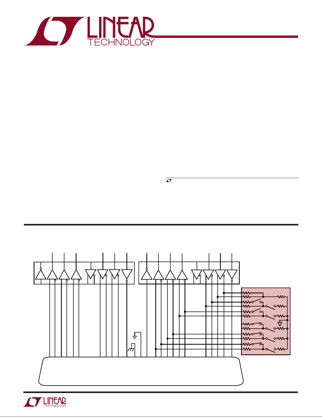
TYPICAL APPLICATION
Daisy-Chained Control Outputs
U
1
Page 2
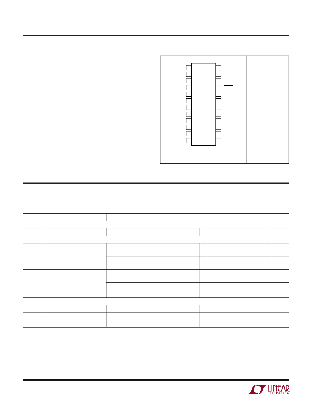
LTC1344
1
2
3
4
5
6
7
8
9
10
11
12
TOP VIEW
G PACKAGE
24-LEAD PLASTIC SSOP
24
23
22
21
20
19
18
17
16
15
14
13
M0
V
EE
R1C
R1B
R1A
R2A
R2B
R2C
R3A
R3B
R3C
GND
M1
M2
DCE/DTE
LATCH
R6B
R6A
R5A
R5B
R4A
R4B
V
CC
GND
WW
W
U
ABSOLUTE MAXIMUM RATINGS
(Note 1)
Positive Supply Voltage (VCC)................................... 7V
Negative Supply Voltage (VEE) ........................... –13.2V
Input Voltage (Logic Inputs) .... VEE – 0.3V to VCC + 0.3V
Input Voltage (Load Inputs) .................................. ±18V
Operating Temperature Range
LTC1344C ............................................... 0°C to 70°C
LTC1344I........................................... –40°C to 85°C
Storage Temperature Range ................ –65°C to 150°C
Lead Temperature (Soldering, 10 sec)................. 300°C
/
PACKAGE
T
JMAX
Consult factory for Military grade parts.
O
RDER I FOR ATIO
= 150°C, θJA = 100°C/W
WU
ORDER PART
NUMBER
LTC1344CG
LTC1344IG
U
ELECTRICAL CHARACTERISTICS
The ● denotes the specifications which apply over the full operating temperature range, otherwise specifications are at TA = 25°.
V
= 5V ±5%, VEE = –5V ±5%, T
CC
SYMBOL PARAMETER CONDITIONS MIN TYP MAX UNITS
Supplies
I
CC
Terminator Pins
R
V.35
R
V.11
I
LEAK
Logic Inputs
V
IH
V
IL
I
IN
Note 1: Absolute Maximum Ratings are those values beyond which the life
of a device may be impaired.
Note 2: All currents into device pins are positive; all currents out of device
pins are negative. All voltages are reference to ground unless otherwise
specified.
Supply Current All Digital Pins = GND or V
Differential Mode Impedance All Loads (Figure 1), – 2V ≤ VCM ≤ 2V (Commercial) ● 90 103 110 Ω
Common Mode Impedance All Loads (Figure 2), – 2V ≤ V
Differential Mode Impedance All Loads (Figure 1), – 7V ≤ VCM ≤ 7V (Commercial) 100 104 Ω
High Impedance Leakage Current All Loads, –7V ≤ VCM ≤ 7V (Commercial) ● ±1 ±50 µA
Input High Voltage All Logic Input Pins ● 2V
Input Low Voltage All Logic Input Pins ● 0.8 V
Input Current All Logic Input Pins ● ±10 µA
A
= T
MIN
to T
(Notes 2, 3) unless otherwise noted.
MAX
CC
≤ 2V (Commercial) ● 135 153 165 Ω
CM
All Loads (Figure 1), – 2V ≤ VCM ≤ 2V (Industrial) ● 90 104 125 Ω
All Loads (Figure 2), – 2V ≤ V
All Loads (Figure 1), V
All Loads (Figure 1), V
CM
CM
≤ 2V (Industrial) ● 130 153 170 Ω
CM
= 0V (Commercial) ● 100 104 110 Ω
= 0V (Industrial) ● 95 104 125 Ω
Note 3: All typicals are given at VCC = 5V, VEE = –5V, T
● 200 700 µA
= 25°C.
A
2
Page 3
W
VCC VOLTAGE (V)
103
DIFFERENTIAL MODE IMPEDANCE (Ω)
104
105
1344 G03
4.6 4.8 5.0 5.2 5.4
U
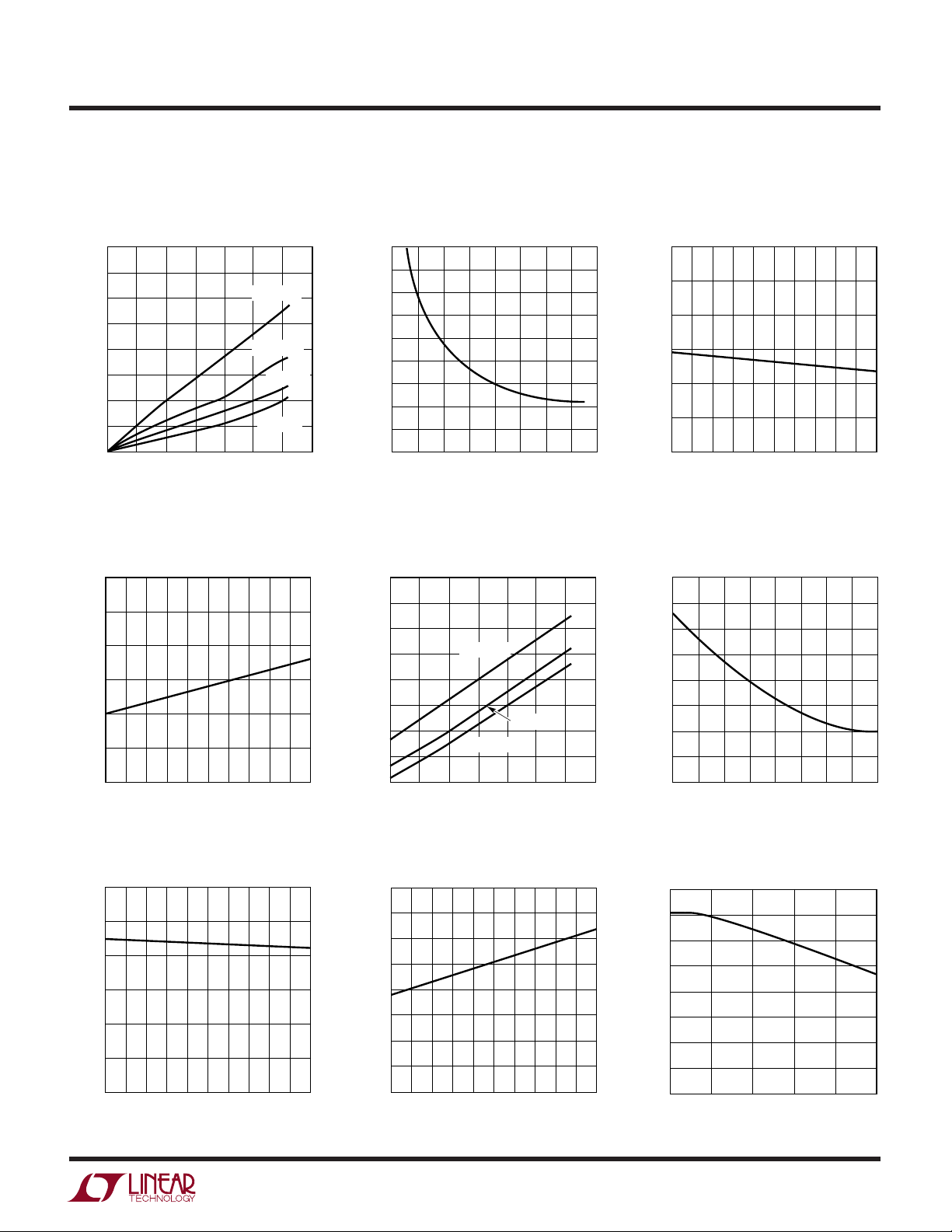
TYPICAL PERFORMANCE CHARACTERISTICS
LTC1344
V.11 or V.35 Differential Mode
Impedance vs Temperature
120
115
110
105
DIFFERENTIAL MODE IMPEDANCE (Ω)
100
–40
–20 0 40
20
TEMPERATURE (°C)
V.11 or V.35 Differential Mode
Impedance vs Negative Supply
Voltage (VEE)
105
VCM = –7V
= –2V
V
CM
VCM = 0V
V
= 7V
CM
60 80 100
1344 G01
V.11 or V.35 Differential Mode
Impedance vs Common Mode
Voltage
108
106
104
102
DIFFERENTIAL MODE IMPEDANCE (Ω)
100
–8
–6 –4 –2 0 2 4 8
COMMON MODE VOLTAGE (V)
V.35 Common Mode Impedance
vs Temperature
165
160
VCM = –2V
V.11 or V.35 Differential Mode
Impedance vs Supply Voltage
(VCC)
6
1344 G02
V.35 Common Mode Impedance
vs Common Mode Voltage
158
156
104
DIFFERENTIAL MODE IMPEDANCE (Ω)
103
–5.4 – 5.2 –5.0 –4.8 – 4.6
V.35 Common Mode Impedance
vs Supply Voltage (VCC)
153
152
COMMON MODE IMPEDANCE (Ω)
151
4.6 4.8 5.0 5.2 5.4
VEE VOLTAGE (V)
VCC VOLTAGE (V)
1344 G04
1344 G07
155
150
COMMON MODE IMPEDANCE (Ω)
145
–20 0 40
–40
TEMPERATURE (°C)
VCM = 0V
VCM = 2V
20
V.35 Common Mode Inpedance
vs Negative Supply Voltage (VEE)
154
153
152
151
COMMON MODE IMPEDANCE (Ω)
150
–5.4
–5.2
–5.0
VEE VOLTAGE (V)
60 80 100
1344 G05
–4.8
–4.6
1344 G08
154
152
COMMON MODE IMPEDANCE (Ω)
150
–2
–1
COMMON MODE VOLTAGE (V)
0
Supply Current vs Temperature
310
290
270
250
230
210
SUPPLY CURRENT (µA)
190
170
150
–20 10 40 70 100
–50
TEMPERATURE (°C)
1
2
1344 G06
1344 G09
3
Page 4
LTC1344
PIN FUNCTIONS
UUU
M0 (Pin 1): TTL Level Mode Select Input. The data on M0
is latched when LATCH is high.
VEE (Pin 2): Negative Supply Voltage Input. Can connect
directly to the LTC1343 VEE pin.
R1C (Pin 3): Load 1 Center Tap.
R1B (Pin 4): Load 1 Node B.
R1A (Pin 5): Load 1 Node A.
R2A (Pin 6): Load 2 Node A.
R2B (Pin 7): Load 2 Node B.
R2C (Pin 8): Load 2 Center Tap.
R3A (Pin 9): Load 3 Node A.
R2B (Pin 10): Load 2 Node B.
R3C (Pin 11): Load 3 Center Tap.
GND (Pin 12): Ground Connection for Load 1 to Load 3.
GND (Pin 13): Ground Connection for Load 4 to Load 6.
V
(Pin 14): Positive Supply Input. 4.75V ≤ VCC ≤ 5.25V.
CC
R4B (Pin 15): Load 4 Node B.
R4A (Pin 16): Load 4 Node A.
R5B (Pin 17): Load 5 Node B.
R5A (Pin 18): Load 5 Node A.
R6A (Pin 19): Load 6 Node A.
R6B (Pin 20): Load 6 Node B.
LATCH (Pin 21): TTL Level Logic Signal Latch Input. When
it is low the input buffers on M0, M1, M2 and DCE/DTE are
transparent. When it is high the logic pins are latched into
their respective input buffers. The data latch allows the
select lines to be shared between multiple I/O ports.
DCE/DTE (Pin 22): TTL Level Mode Select Input. The DCE
mode is selected when it is high and DTE mode when low.
The data on DCE/DTE is latched when LATCH is high.
M2 (Pin 23): TTL Level Mode Select Input 1. The data on
M2 is latched when LATCH is high.
M1 (Pin 24): TTL Level Mode Select Input 2. The data on
M1 is latched when LATCH is high.
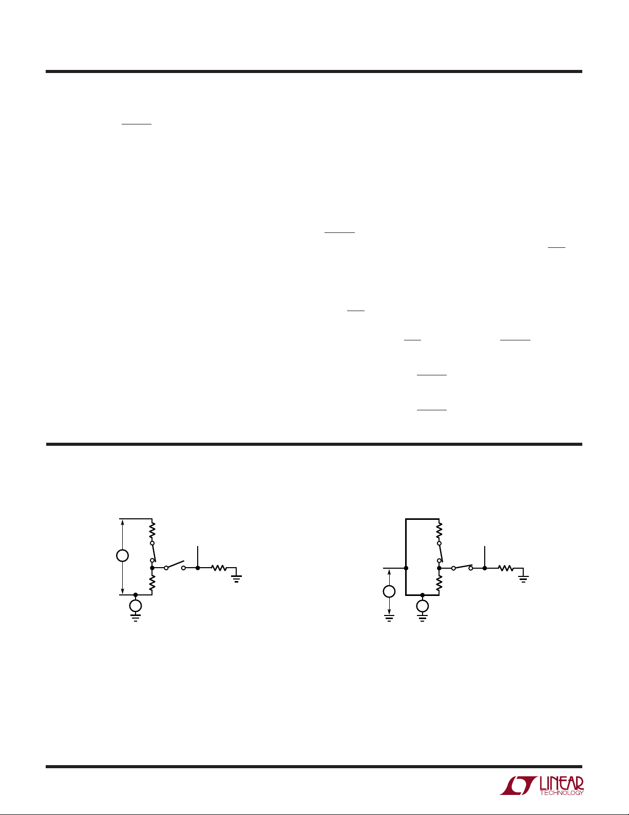
TEST CIRCUITS
A
Ω
B
Figure 1. Differential V.11 or V.35 Impedance Measurement Figure 2. V.35 Common Mode Impedance Measurement
S1
ON
±7V OR ±2V
V
R1
51.5Ω
R2
51.5Ω
S2
OFF
R1
C
R3
124Ω
1344 F01
A, B
Ω
51.5Ω
S1
ON
R2
51.5Ω
±2V
V
S2
ON
C
R3
124Ω
1344 F02
4
Page 5

LTC1344
W U
ODE SELECTIO
LTC1344
MODE NAME DCE/DTE M2 M1 M0 R1 R2 R3 R4 R5 R6
V.10/RS423 X 000ZZZZZZ
RS530A 0 001ZZZV.11 V.11 V.11
1 001ZZZZV.11 V.11
Reserved 0 010ZZZV.11 V.11 V.11
1 0 1 0 V.11 V.11 V.11 Z Z Z
X.21 0 011ZZZV.11 V.11 V.11
1 011ZZZZV.11 V.11
V.35 0 1 0 0 V.35 V.35 Z V.35 V.35 V.35
1 1 0 0 V.35 V.35 V.35 Z V.35 V.35
RS530/RS449/V.36 0 101ZZZV.11 V.11 V.11
1 101ZZZZV.11 V.11
V.28/RS232 X 110ZZZZZZ
No Cable X 1 1 1 V.11 V.11 V.11 V.11 V.11 V.11
X = don’t care, 0 = logic low, 1 = logic high
A
B
ON
R1
51.5Ω
S1
R2
51.5Ω
S2
OFF
C
R3
124Ω
A
B
ON
R1
51.5Ω
S1
R2
51.5Ω
S2
ON
C
R3
124Ω
A
B
OFF
R1
51.5Ω
S1
R2
51.5Ω
S2
OFF
C
R3
124Ω
1344 F03
V.11 Mode V.35 Mode Hi-Z Mode
Figure 3. LTC1344 Modes
5
Page 6

LTC1344
U
WUU
APPLICATIONS INFORMATION
Multiprotocol Cable Termination
One of the most difficult problems facing the designer of
a multiprotocol serial interface is how to allow the transmitters and receivers for different electrical standards to
share connector pins. In some cases the transmitters and
receivers for each interface standard can be simply tied
together and the appropriate circuitry enabled. But the
biggest problem still remains: how to switch the various
cable terminations required by the different standards.
Traditional implementations have included switching resistors with expensive relays or requiring the user to
change termination modules every time the interface
standard has changed. Custom cables have been used
with the termination in the cable head or separate terminations are built on the board, and a custom cable routes the
signals to the appropriate termination. Switching the
terminations using FETs is difficult because the FETs must
remain off even though the signal voltage is beyond the
supply voltage for the FET drivers or the power is off.
The LTC1344 solves the cable termination switching problem via software control. The LTC1344 provides termination for the V.10 (RS423), V.11 (RS422), V.28 (RS232)
and V.35 electrical protocols.
V.10 (RS423) Termination
A typical V.10 unbalanced interface is shown in Figure 4.
A V.10 single-ended generator output A with ground C is
connected to a differential receiver with inputs A' connected to A and input B' connected to the signal return
ground C. The receiver’s ground C' is separate from the
signal return. Usually no cable termination is required for
V.10 interfaces but the receiver inputs must be compliant
with the impedance curve shown in Figure 5.
In V.10 mode, both switches S1 and S2 are turned off so
the only cable termination is the input impedance of the
V.10 receiver.
BALANCED
INTERCONNECTING
CABLE
LTC1344
124Ω
–3V
A
'
B
'
C
'
I
Z
A
C
Figure 4. Typical V.10 Interface
A
51.5Ω
S2
S1
OFF
OFF
51.5Ω
B
C
Z
Figure 5. V.10 Interface Using the LTC1344
–10V
–3.25mA
LOADGENERATOR
CABLE
TERMINATION
RECEIVER
Z
Z
3V 10V
RECEIVER
V.10
1344 F04
3.25mA
V
Z
1344 F05
V.11 (RS422) Termination
A typical V.11 balanced interface is shown in Figure 6. A
V.11 differential generator with outputs A and B with
ground C is connected to a differential receiver with
ground C', inputs A' connected to A, B' connected to B. The
V.11 interface requires a different termination at the re-
ceiver end that has a minimum value of 100Ω. The receiver
inputs must also be compliant with the impedance curve
shown in Figure 7.
In V.11 mode, switch S1 is turned on and S2 is turned off
so the cable is terminated with a 103Ω impedance.
6
Page 7

LTC1344
U
WUU
APPLICATIONS INFORMATION
BALANCED
INTERCONNECTING
CABLE
A
BB
C
A
'
'
C
'
Figure 6. Typical V.11 Interface
A
S2
OFF
LTC1344
124Ω
I
Z
51.5Ω
S1
ON
51.5Ω
B
C
LOADGENERATOR
CABLE
TERMINATION
100Ω
MIN
RECEIVER
Z
Z
RECEIVER
1344 F06
V.11
3.25mA
BALANCED
INTERCONNECTING
CABLE
A
CC'
A
'
LOADGENERATOR
CABLE
TERMINATION
RECEIVER
1344 F08
Figure 8. Typical V.28 Interface
A
V.28
RECEIVER
5k
1344 F09
S1
OFFS2OFF
B
C
51.5Ω
51.5Ω
LTC1344
124Ω
Figure 9. V.28 Interface Using the LTC1344
Z
–10V
–3.25mA
–3V
3V 10V
V
Z
1344 F07
Figure 7. V.11 Interface Using the LTC1344
V.28 (RS232) Termination
A typical V.28 unbalanced interface is shown in Figure 8.
A V.28 single-ended generator output A with ground C is
connected to a single-ended receiver with inputs A' connected to A, ground C' connected via the signal return
ground to C. The V.28 standard requires a 5k terminating
resistor to ground which is included in almost all compliant receivers as shown in Figure 9. Because the termination is included in the receiver, both switches S1 and S2 in
the LTC1344 are turned off.
V.35 Termination
A typical V.35 balanced interface is shown in Figure 10. A
V.35 differential generator with outputs A and B with
ground C is connected to a differential receiver with
ground C', inputs A' connected to A, B' connected to B. The
V.35 interface requires a T-network termination at the
receiver end and the generator end. In V.35 mode both
switches S1 and S2 in the LTC1344 are turned on as
shown in Figure 11.
The differential impedance measured at the connector
must be 100Ω ±10Ω and the impedance between shorted
terminals A' and B' to ground C' must be 150Ω ±15Ω. The
input impedance of the V.35 receiver is connected in
parallel with the T-network inside the LTC1344, which can
cause the overall impedance to fail the specification on the
7
Page 8

LTC1344
U
WUU
APPLICATIONS INFORMATION
BALANCED
INTERCONNECTING
CABLE
TERMINATION
A
'
B
'
C
'
50Ω
50Ω
A
125Ω
B
C
Figure 10. Typical V.35 Interface
A
–7V
ON
LTC1344
S2
124Ω
I
Z
–3V
3V 12V
51.5Ω
S1
ON
51.5Ω
B
C
Z
–0.8mA
CABLE
125Ω
Z
Z
LOADGENERATOR
50Ω
50Ω
V.35
RECEIVER
RECEIVER
1mA
V
Z
1344 F11
1344 F10
A
V.35
DRIVER
LTC1344
124Ω
51.5Ω
S2
ON
51.5Ω
C1
100pF
S1
ON
B
C
1344 F12
Figure 12. V.35 Driver Using the LTC1344
and B to ground C must be 150Ω ±15Ω. For the generator
termination, switches S1 and S2 are both on and the top
side of the center resistor is brought out to a pin so it can
be bypassed with an external capacitor to reduce common
mode noise as shown in Figure 12.
Any mismatch in the driver rise and fall times or skew in
the driver propagation delays will force current through
the center termination resistor to ground causing a high
frequency common mode spike on the A and B terminals.
The common mode spike can cause EMI problems that are
reduced by capacitor C1 which shunts much of the common mode energy to ground rather than down the cable.
The LATCH Pin
Figure 11. V.35 Receiver Using the LTC1344
low side. However, all of Linear Technology’s V.35 receivers meet the RS485 input impedance specification as
shown in Figure 11, which insures compliance with the
V.35 specification when used with the LTC1344.
The generator differential impedance must be 50Ω to
150Ω and the impedance between shorted terminals A
8
The LATCH pin (21) allows the select lines (M0, M1, M2
and DCE/DTE) to be shared with multiple LTC1344s, each
with its own LATCH signal. When the LATCH pin is held
low the select line input buffers are transparent. When the
LATCH pin is pulled high, the select line input buffers latch
the state of the Select pins so that changes on the select
lines are ignored until LATCH is pulled low again. If the
latch feature is not used, the LATCH pin should be tied to
ground.
Page 9

U
TYPICAL APPLICATIONS N
LTC1344
Figure 13 shows a typical application for the LTC1344
using the LTC1343 mixed mode transceiver chip to generate the clock and data signals for a serial interface. The
LTC1344 VEE supply is generated from the LTC1343
charge pump and the select lines M0, M1, M2, DCE and
100pF
3
1
24
23
22
21
5V
M0
M1
M2
DCE/DTE
LATCH
V
CC
LTC1344
V
EE
14
2
5
M0
M1
M2
DCE/DTE
LATCH
LATCH are shared by both chips. Each driver output and
receiver input is connected to one of the LTC1344 termination ports. Each electrical protocol can then be chosen
using the digital select lines.
100pF
8
4
6
100pF
11
12 13
7
9
161518 17 19 20
10
C1
1µF
17
18
19
21
22
6
7
9
13
14
15
3842
LTC1343
M0
M1
M2
DCE/DTE
LATCH
C2
+
3.3µF
38
37
36
35
34
33
32
31
30
29
28
27
Figure 13. Typical Application Using the LTC1344
DTE DCE
+
TXD
TXD–RXD
SCTE+TXC
SCTE–TXC
NC RXC
NC RXC
RXC+NC
RXC
TXC
TXC–SCTE
RXD+TXD
RXD–TXD
RXD
–
NC
+
SCTE
+
–
+
–
+
–
+
–
+
–
1344 F13
9
Page 10

LTC1344
U
TYPICAL APPLICATIONS N
Controller Selectable Multiprotocol DTE Port with DB-25 Connector
V
CC
5V
1µF
100k
1
2
C1
4
CHARGE
PUMP
3
8
C5
1µF
R1
10
12
13
14
15
16
20
22
11
25
40
23
5
6
7
9
LTC1343
D1
D2
D3
D4
R1
R2
R3
R4
CTRL
LATCH
INVERT
423 SET
GND
LB
DTE_LL/DCE_TM
DTE_TXD/DCE_RXD
DTE_SCT/DEC_RXC
DTE_TXC/DCE_TXC
DTE_RXC/DCE_SCTE
DTE_RXD/DCE_TXD
DTE_TM/DCE_LL
C3
1µF
DCE
C6
100pFC7100pF
14
V
CC
44
C2
43
1µF
42
41
39
38
37
36
35
34
33
32
31
30
29
28
27
26
21
19
M2
18
M1
17
M0
24
EC
2
V
EE
C4
+
3.3µF
V
CC
C8
100pF
13
121138
LTC1344
21
LATCH
DCE/
DTE
19171815161097645
20 22 23 24 1
M0M1M2
DB-25 CONNECTOR
DTE DCE
18
LL A
2
TXD A
14
TXD B
24
SCTE A
11
SCTE B
15
TXC A
12
TXC B
17
RXC A
9
RXC B
3
RXD A
16
RXD B
25
TM A
7
SGND
TM A
RXD A
RXD B
RXC A
RXC B
TXC A
TXC B
SCTE A
SCTE B
TXD A
TXD B
LL A
DTE_RL/DCE_RL
DTE_RTS/DCE_CTS
DTE_DTR/DCE_DSR
DTE_DCD/DCE_DCD
DTE_DSR/DCE_DTR
DTE_CTS/DCE_RTS
LATCH
DCE/DTE
SHIELD
1
21
4
19
20
23
8
10
6
22
5
13
RL A
RTS A
RTS B
DTR A
DTR B
DCD A
DCD B
DSR A
DSR B
CTS A
CTS B
RL A
CTS A
CTS B
DSR A
DSR B
DCD A
DCD B
DTR A
DTR B
RTS A
RTS B
1344 TA02
1µF
100k
1
2
C9
4
CHARGE
3
8
C12
1µF
R2
10
12
13
14
15
16
20
22
11
25
40
23
5
6
7
9
LTC1343
CTRL
LATCH
INVERT
423 SET
GND
LB
C11
1µF
V
CC
V
CC
LB
M2
M1
M0
PUMP
D1
D2
D3
D4
R1
R2
R3
R4
DCE
44
C10
43
1µF
42
C13
+
3.3µF
41
39
38
37
36
35
34
33
32
31
30
29
28
27
26
21
19
M2
18
M1
17
M0
24
EC
10
Page 11

U
TYPICAL APPLICATIONS N
Cable Selectable Multiprotocol DTE Port with DB-25 Connector
V
CC
5V
1µF
1µF
100k
100k
1
2
C1
4
CHARGE
PUMP
3
8
C5
1µF
R1
C9
C12
1µF
R2
LTC1343
5
D1
6
D2
7
D3
9
D4
10
12
13
R1
14
R2
15
R3
16
R4
20
CTRL
22
LATCH
11
INVERT
25
423 SET
40
GND
23
LB
1
2
4
3
8
5
6
7
9
10
12
13
14
15
16
20
CTRL
22
LATCH
11
INVERT
25
423 SET
40
GND
23
LB
CHARGE
PUMP
LTC1343
D1
D2
D3
D4
R1
R2
R3
R4
DCE
DCE
DTE_TXD/DCE_RXD
DTE_SCTE/DEC_RXC
DTE_TXC/DCE_TXC
DTE_RXC/DCE_SCTE
DTE_RXD/DCE_TXD
DTE_RTS/DCE_CTS
DTE_DTR/DCE_DSR
DTE_DCD/DCE_DCD
DTE_DSR/DCE_DTR
DTE_CTS/ DCE_RTS
C3
1µF
C11
1µF
V
CC
V
CC
LB
LTC1344
C6
100pFC7100pF
14
V
CC
44
C2
43
1µF
42
41
39
38
37
36
35
34
33
32
31
30
29
28
27
26
21
19
M2
18
M1
17
M0
24
EC
44
43
42
41
39
38
37
36
35
34
33
32
31
30
29
28
27
26
21
19
M2
18
M1
17
M0
24
EC
2
V
EE
C4
+
3.3µF
V
CC
V
CC
C10
1µF
C13
+
3.3µF
V
CC
C8
100pF
13
121138
V
V
V
CC
CC
CC
R3
10k
CABLE WIRING FOR MODE SELECTION
MODE PIN 18 PIN 21
V.35 PIN 7 PIN 7
EIA-530, RS449, NC PIN 7
V.36, X.21
RS232 PIN 7 NC
R4
10k
R5
10k
LTC1344
LATCH
DCE/
DTE
19171815161097645
20 22 23 24 1
V
CC
CABLE WIRING FOR DTE/DCE
SELECTION
MODE PIN 25
DTE PIN 7
DCE NC
M0M1M2
21
DB-25 CONNECTOR
2
TXD A
14
TXD B
24
SCTE A
11
SCTE B
15
TXC A
12
TXC B
17
RXC A
9
RXC B
3
RXD A
16
RXD B
7
SGND
1
SHIELD
25
DCE/DTE
21
M1
18
M0
4
RTS A
19
RTS B
20
DTR A
23
DTR B
8
DCD A
10
DCD B
6
DSR A
22
DSR B
5
CTS A
13
CTS B
DTE DCE
RXD A
RXD B
RXC A
RXC B
TXC A
TXC B
SCTE A
SCTE B
TXD A
TXD B
CTS A
CTS B
DSR A
DSR B
DCD A
DCD B
DTR A
DTR B
RTS A
RTS B
1344 TA03
Information furnished by Linear Technology Corporation is believed to be accurate and reliable.
However, no responsibility is assumed for its use. Linear Technology Corporation makes no representation that the interconnection of its circuits as described herein will not infringe on existing patent rights.
11
Page 12

LTC1344
PACKAGE DESCRIPTION
U
Dimensions in inches (millimeters) unless otherwise noted.
G Package
24-Lead Plastic SSOP (0.209)
(LTC DWG # 05-08-1640)
8.07 – 8.33*
(0.318 – 0.328)
2122 18 17 16 15 14
19202324
13
7.65 – 7.90
(0.301 – 0.311)
5.20 – 5.38**
(0.205 – 0.212)
° – 8°
0
0.13 – 0.22
(0.005 – 0.009)
NOTE: DIMENSIONS ARE IN MILLIMETERS
DIMENSIONS DO NOT INCLUDE MOLD FLASH. MOLD FLASH
*
SHALL NOT EXCEED 0.152mm (0.006") PER SIDE
DIMENSIONS DO NOT INCLUDE INTERLEAD FLASH. INTERLEAD
**
FLASH SHALL NOT EXCEED 0.254mm (0.010") PER SIDE
0.55 – 0.95
(0.022 – 0.037)
12345678 9 10 11 12
0.65
(0.0256)
BSC
0.25 – 0.38
(0.010 – 0.015)
1.73 – 1.99
(0.068 – 0.078)
0.05 – 0.21
(0.002 – 0.008)
G24 SSOP 1098
RELATED PARTS
PART NUMBER DESCRIPTION COMMENTS
LTC1334 Single Supply RS232/RS485 Transceiver 2 RS485 Dr/Rx or 4 RS232 Dr/Rx Pairs
LTC1343 Multiprotocol Serial Transceiver Software Selectable Mulitprotocol Interface
LTC1345 Single Supply V.35 Transceiver 3 Dr/3 Rx for Data and CLK Signals
LTC1346A Dual Supply V.35 Transceiver 3 Dr/3 Rx for Data and CLK Signals
LTC1344A Multiprotocol Cable Terminator, Pin Compatible to LTC1344 Allows Separate RS449 Mode
LTC1543 Multiprotocol Serial Transceiver 3 Dr/3 Rx for Data and CLK Signals
LTC1544 Multiprotocol Serial Transceiver 4 Dr/4 Rx for Control Signals and LL
LTC1545 Multiprotocol Serial Transceiver 5 Dr/5 Rx for Control Signals, LL, RL amd TM
12
Linear Technology Corporation
1630 McCarthy Blvd., Milpitas, CA 95035-7417
(408) 432-1900 ● FAX: (408) 434-0507
●
www.linear-tech.com
1344fa LT/TP 0300 2K REV A • PRINTED IN USA
LINEAR TECHNOLOGY CORPORATION 1996
 Loading...