

Page 1
FEATURES
LTC1334
Single 5V RS232/RS485
Multiprotocol Transceiver
U
DESCRIPTIO
■
Four RS232 Transceivers or Two RS485
Transceivers on One Chip
■
Operates from a Single 5V Supply
■
Withstands Repeated ±10kV ESD Pulses
■
Uses Small Charge Pump Capacitors: 0.1µF
■
Low Supply Current: 8mA Typical
■
10µA Supply Current in Shutdown
■
Self-Testing Capability in Loopback Mode
■
Power-Up/Down Glitch-Free Outputs
■
Driver Maintains High Impedance in Three-State,
Shutdown or with Power Off
■
Thermal Shutdown Protection
■
Receiver Inputs Can Withstand ±25V
U
APPLICATIO S
■
Low Power RS485/RS422/RS232/EIA562 Interface
■
Software-Selectable Multiprotocol Interface Port
■
Cable Repeaters
■
Level Translators
The LTC®1334 is a low power CMOS
ceiver featuring two
reconfigurable interface ports. It can
bidirectional trans-
be configured as two RS485 differential ports, as two dual
RS232 single-ended ports or as one RS485 differential
port and one dual RS232 single-ended port. An onboard
charge pump requires four 0.1µF capacitors to generate
boosted positive and negative supplies, allowing the RS232
drivers to meet the RS232 ±5V output swing requirement
with only a single 5V supply. A shutdown mode reduces
the ICC supply current to 10µA.
The RS232 transceivers are in full compliance with RS232
specifications. The RS485 transceivers are in full compliance with RS485 and RS422 specifications. All interface
drivers feature short-circuit and thermal shutdown protection. An enable pin allows RS485 driver outputs to be
forced into high impedance, which is maintained even
when the outputs are forced beyond supply rails or power
is off. Both driver outputs and receiver inputs feature
±10kV ESD protection. A loopback mode allows the driver
outputs to be connected back to the receiver inputs for
diagnostic self-test.
, LTC and LT are registered trademarks of Linear Technology Corporation.
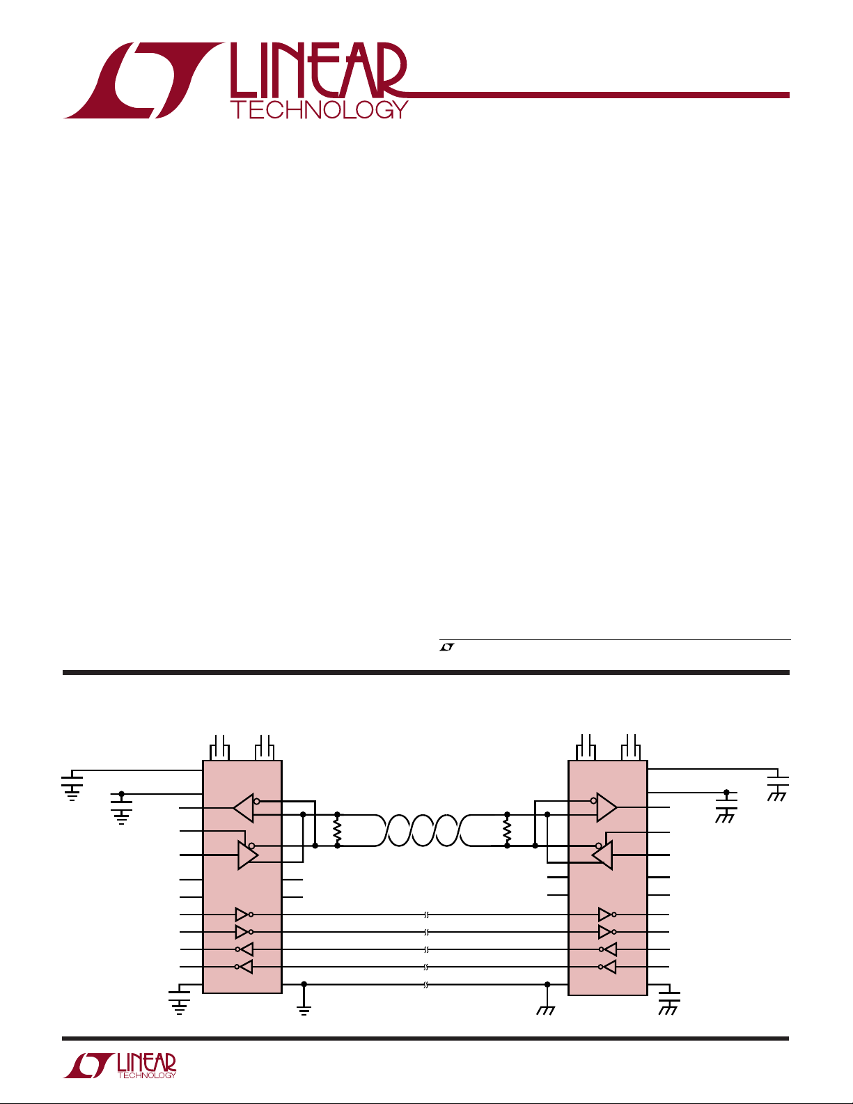
TYPICAL APPLICATIO
12
3
LTC1334
DR IN
DR IN
DR IN
26
24
23
22
21
5V
20
5V
19
18
17
16
15
V
CC1
5V
RX OUT
DR ENABLE
RX OUT
RX OUT
U
2728
LTC1334
4
5
6
7
8
9
11
10
13
12
14
120Ω
5V
0V
ALL CAPACITORS: 0.1µF MONOLITHIC CERAMIC TYPE
RS485 INTERFACE
4000-FT 24-GAUGE TWISTED PAIR
RS232 INTERFACE
120Ω
13
12
11
10
9
5V
8
0V
4
5
6
7
14
212827
3
26
17
18
19
21
20
24
25
22
23
15
RX OUT
DR ENABLE
DR IN
5V
5V
RX OUT
RX OUT
DR IN
DR IN
V
CC2
5V
LTC1334 • TA01
1
Page 2
LTC1334
A
S
(Note 1)
W
O
LUTEXI TIS
A
WUW
U
ARB
G
Supply Voltage (VCC) ............................................. 6.5V
Input Voltage
Drivers ................................... –0.3V to (VCC + 0.3V)
Receivers ............................................. – 25V to 25V
ON/OFF, LB, SEL1, SEL2 ........ –0.3V to (VCC + 0.3V)
Output Voltage
Drivers ................................................. – 18V to 18V
Receivers ............................... –0.3V to (VCC + 0.3V)
Short-Circuit Duration
Output ........................................................ Indefinite
VDD, VEE, C1+, C1–, C2+, C2–.......................... 30 sec
Operating Temperature Range
Commercial........................................... 0°C to 70°C
Industrial............................................ –40°C to 85°C
Storage Temperature Range ................ –65°C to 150°C
Lead Temperature (Soldering, 10 sec)................ 300°C
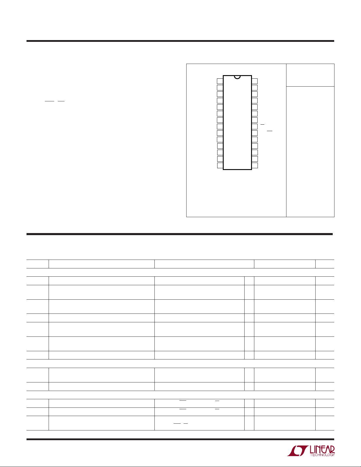
PACKAGE
+
1
C1
–
2
C1
3
V
DD
4
A1
5
B1
6
Y1
7
Z1
8
SEL1
9
SEL2
10
Z2
11
Y2
12
B2
13
A2
14
GND
G PACKAGE
28-LEAD PLASTIC SSOP
28-LEAD PLASTIC SO WIDE
T
= 125°C, θJA = 90°C/W (G)
JMAX
T
= 125°C, θJA = 56°C/W (NW)
JMAX
T
= 125°C, θJA = 85°C/W (SW)
JMAX
/
O
RDER I FOR ATIO
TOP VIEW
28-LEAD PDIP WIDE
SW PACKAGE
28
C2
27
C2
26
V
CC
25
R
B1
24
R
A1
23
DZ1/DE1
22
D
Y1
21
LB
20
ON/OFF
19
D
Y2
18
DZ2/DE2
17
R
A2
16
R
B2
15
V
EE
NW PACKAGE
+
–
ORDER PART
LTC1334CG
LTC1334CNW
LTC1334CSW
LTC1334IG
LTC1334ISW
WU
U
NUMBER
Consult factory for Military grade parts.
DC ELECTRICAL CHARACTERISTICS
The ● denotes specifications which apply over the full operating
temperature range, otherwise specifications are at TA = 25°C. VCC = 5V, C1 = C2 = C3 = C4 = 0.1µF (Notes 2, 3)
SYMBOL PARAMETER CONDITIONS MIN TYP MAX UNITS
RS485 Driver (SEL1 = SEL2 = High)
V
OD1
V
OD2
∆V
OD
V
OC
∆VOC Change in Magnitude of Driver Common Mode Figure 1, R = 27Ω or R = 50Ω ● 0.2 V
I
OSD
I
OZD
RS232 Driver (SEL1 = SEL2 = Low)
V
O
I
OSD
Driver Inputs and Control Inputs
V
IH
V
IL
I
IN
Differential Driver Output Voltage (Unloaded) IO = 0 ● 6V
Differential Driver Output Voltage (With Load) Figure 1, R = 50Ω (RS422) ● 2.0 6 V
Figure 1, R = 27Ω (RS485) ● 1.5 6 V
Change in Magnitude of Driver Differential Figure 1, R = 27Ω or R = 50Ω ● 0.2 V
Output Voltage for Complementary Output States
Driver Common Mode Output Voltage Figure 1, R = 27Ω or R = 50Ω ● 3V
Output Voltage for Complementary Output States
Driver Short-Circuit Current –7V ≤ VO ≤ 12V, VO = High ● 35 250 mA
–7V ≤ V
Three-State Output Current (Y, Z) –7V ≤ VO ≤ 12V ● ±5 ±500 µA
Output Voltage Swing Figure 4, RL = 3k, Positive ● 5 6.5 V
Figure 4, R
Output Short-Circuit Current VO = 0V ● ±60 mA
Input High Voltage D, DE, ON/OFF, SEL1, SEL2, LB ● 2V
Input Low Voltage D, DE, ON/OFF, SEL1, SEL2, LB ● 0.8 V
Input Current D, SEL1, SEL2 ● ±10 µA
DE, ON/OFF, LB
≤ 12V, VO = Low (Note 4) ● 10 250 mA
O
= 3k, Negative ● –5 –6.5 V
L
● –4 –15 µA
2
Page 3
LTC1334
DC ELECTRICAL CHARACTERISTICS
The ● denotes specifications which apply over the full operating
temperature range, otherwise specifications are at TA = 25°C. VCC = 5V, C1 = C2 = C3 = C4 = 0.1µF (Notes 2, 3)
SYMBOL PARAMETER CONDITIONS MIN TYP MAX UNITS
RS485 Receiver (SEL1 = SEL2 = High)
V
TH
∆V
TH
I
IN
R
IN
RS232 Receiver (SEL1 = SEL2 = Low)
V
TH
∆V
TH
R
IN
Receiver Output
V
OH
V
OL
I
OSR
I
OZR
R
OB
Power Supply Generator
V
DD
V
EE
Power Supply
I
CC
Differential Input Threshold Voltage –7V ≤ VCM ≤ 12V, LTC1334C ● –0.2 0.2 V
–7V ≤ V
≤ 7V, LTC1334I ● –0.3 0.3 V
CM
Input Hysteresis VCM = 0V 70 mV
Input Current (A, B) VIN = –7V ● – 0.8 mA
= 12V ● 1.0 mA
V
IN
Input Resistance –7V ≤ VIN ≤ 12V ● 12 24 kΩ
Receiver Input Threshold Voltage Input Low Threshold ● 0.8 V
Input High Threshold
● 2.4 V
Receiver Input Hysteresis 0.6 V
Receiver Input Resistance VIN = ±10V 3 5 7 kΩ
Receiver Output High Voltage IO = –3mA, VIN = 0V, SEL1 = SEL2 = Low ● 3.5 4.6 V
Receiver Output Low Voltage IO = 3mA, VIN = 3V, SEL1 = SEL2 = Low ● 0.2 0.4 V
Short-Circuit Current 0V ≤ VO ≤ V
CC
● 785mA
Three-State Output Current ON/OFF = Low ● ±10 µA
Inactive “B” Output Pull-Up Resistance (Note 5) ON/OFF = High, SEL1 = SEL2 = High 50 kΩ
VDD Output Voltage No Load, ON/OFF = High 8.5 V
= –10mA, ON/OFF = High 7.6 V
I
DD
VEE Output Voltage No Load, ON/OFF = High – 7.7 V
= 10mA, ON/OFF = High –6.9 V
I
EE
VCC Supply Current No Load, SEL1 = SEL2 = High ● 825 mA
No Load Shutdown, ON/OFF = 0V
● 10 100 µA
AC ELECTRICAL CHARACTERISTICS
The ● denotes specifications which apply over the full operating
temperature range, otherwise specifications are at TA = 25°C. VCC = 5V, C1 = C2 = C3 = C4 = 0.1µF (Notes 2, 3)
SYMBOL PARAMETER CONDITIONS MIN TYP MAX UNITS
RS232 Mode (SEL1 = SEL2 = Low)
SR Slew Rate Figure 4, RL = 3k, CL = 15pF ● 30 V/µs
t
t
t
t
t
T
PLH
PHL
PLH
PHL
Figure 4, R
Transition Time Figure 4, RL = 3k, CL = 2500pF ● 0.22 1.9 3.1 µs
Driver Input to Output Figures 4, 9, RL = 3k, CL = 15pF ● 0.6 4 µs
Driver Input to Output Figures 4, 9, RL = 3k, CL = 15pF ● 0.6 4 µs
Receiver Input to Output Figures 5, 10 ● 0.3 6 µs
Receiver Input to Output Figures 5, 10 ● 0.4 6 µs
= 3k, CL = 1000pF ● 4V/µs
L
RS485 Mode (SEL1 = SEL2 = High)
t
PLH
t
PHL
t
SKEW
tr, t
f
Driver Input to Output Figures 2, 6, RL = 54Ω, CL = 100pF ● 20 40 70 ns
Driver Input to Output Figures 2, 6, RL = 54Ω, CL = 100pF ● 20 40 70 ns
Driver Output to Output Figures 2, 6, RL = 54Ω, CL = 100pF ● 515 ns
Driver Rise and Fall Time Figures 2, 6, RL = 54Ω, CL = 100pF ● 31540 ns
3
Page 4
LTC1334
AC ELECTRICAL CHARACTERISTICS
The ● denotes specifications which apply over the full operating
temperature range, otherwise specifications are at TA = 25°C. VCC = 5V, C1 = C2 = C3 = C4 = 0.1µF (Notes 2, 3)
SYMBOL PARAMETER CONDITIONS MIN TYP MAX UNITS
RS485 Mode (SEL1 = SEL2 = High)
t
ZL
t
ZH
t
LZ
t
HZ
t
PLH
t
PHL
t
SKEW
Note 1: Absolute Maximum Ratings are those values beyond which the
safety of the device cannot be guaranteed.
Note 2: All currents into device pins are positive; all currents out of device
pins are negative. All voltages are referenced to device ground unless
otherwise specified.
Note 3: All typicals are given at VCC = 5V, C1 = C2 = C3 = C4 = 0.1µF
and T
Driver Enable to Output Low Figures 3, 7, CL = 100pF, S1 Closed ● 50 90 ns
Driver Enable to Output High Figures 3, 7, CL = 100pF, S2 Closed ● 50 90 ns
Driver Disable from Low Figures 3, 7, CL = 15pF, S1 Closed ● 50 90 ns
Driver Disable from High Figures 3, 7, CL = 15pF, S2 Closed ● 60 90 ns
Receiver Input to Output Figures 2, 8, RL = 54Ω, CL = 100pF ● 20 60 140 ns
Receiver Input to Output Figures 2, 8, RL = 54Ω, CL = 100pF ● 20 70 140 ns
Differential Receiver Skew, t
PLH
– t
Figures 2, 8, R
PHL
= 54Ω, CL = 100pF 10 ns
L
Note 4: Short-circuit current for RS485 driver output low state folds back
above VCC. Peak current occurs around VO = 3V.
Note 5: The “B” RS232 receiver output is disabled in RS485 mode
(SEL1 = SEL2 = high). The unused output driver goes into a high
impedance mode and has a resistor to VCC. See Applications Information
section for more details.
= 25°C.
A
W
U
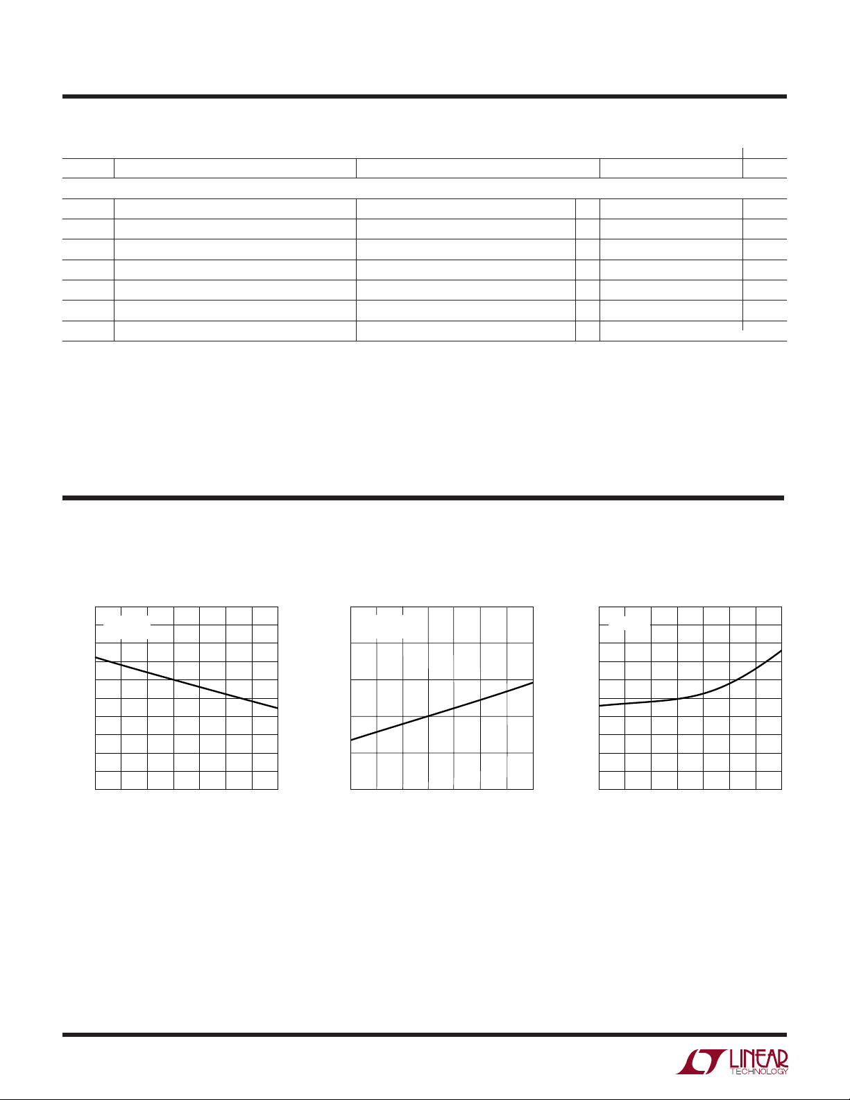
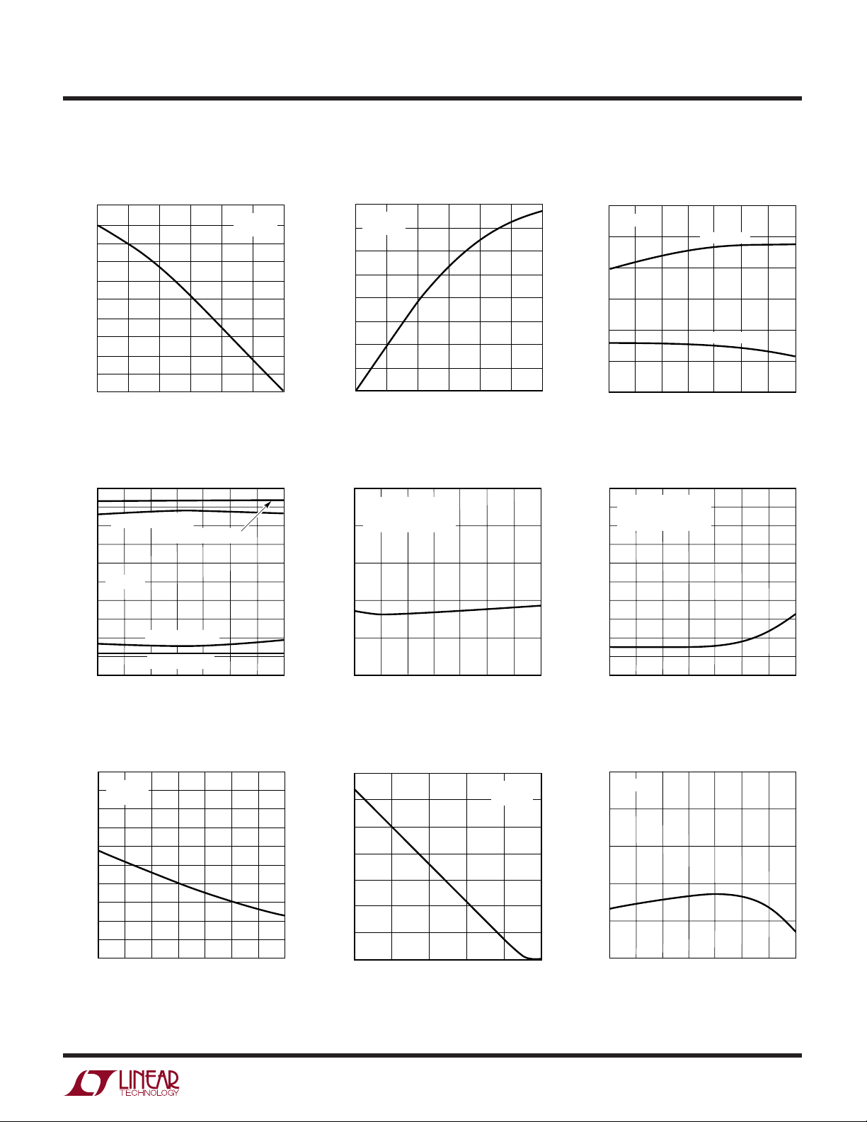
TYPICAL PERFORMANCE CHARACTERISTICS
Receiver Output High Voltage
vs Temperature
5.0
I
= 3mA
OUT
4.9
4.8
4.7
4.6
4.5
4.4
4.3
OUTPUT VOLTAGE (V)
4.2
4.1
4.0
–50
= 5V
V
CC
–25
0
TEMPERATURE (°C)
50
25
75
100
LTC1334 • TPC01
125
Receiver Output Low Voltage
vs Temperature
0.5
I
= 3mA
OUT
V
= 5V
CC
0.4
0.3
0.2
OUTPUT VOLTAGE (V)
0.1
0
–50
0
–25
TEMPERATURE (°C)
50
25
75
100
LTC1334 • TPC02
125
RS485 Receiver Skew
t
– t
PLH
VCC = 5V
–25
PHL
0
TEMPERATURE (°C)
20
18
16
14
12
10
TIME (ns)
8
6
4
2
0
–50
vs Temperature
50
25
75
100
LTC1334 • TPC03
125
4
Page 5
W
TEMPERATURE (°C)
–50
INPUT THRESHOLD VOLTAGE (V)
2.0
1.8
1.6
1.4
1.2
1.0
0.8
25 75
LTC1334 • TPC06
–25 0
50 100 125
INPUT HIGH
INPUT LOW
VCC = 5V
TEMPERATURE (°C)
–50
SUPPLY CURRENT (mA)
10
9
8
7
6
5
4
3
2
1
0
0
50
75
LTC1334 • TPC09
–25
25
100
125
VCC = 5V
NO LOAD
SEL 1 = SEL 2 = HIGH
U
TYPICAL PERFORMANCE CHARACTERISTICS
LTC1334
Receiver Output Current
vs Output High Voltage
20
18
16
14
12
10
8
6
OUTPUT CURRENT (mA)
4
2
0
2.0
2.5
3.5 4.0
3.0
OUTPUT VOLTAGE (V)
Charge Pump Output Voltage
vs Temperature
10
8
VDD (–10mA LOAD)
6
4
2
VCC = 5V
0
–2
–4
OUTPUT VOLTAGE (V)
–6
–8
–10
–50
–25
VDD (NO LOAD)
VEE (10mA LOAD)
VEE (NO LOAD)
0
TEMPERATURE (°C)
50
25
TA = 25°C
V
CC
75
= 5V
4.5
LTC1334 • TPC04
100
LTC1334 • TPC07
125
5.0
Receiver Output Current
vs Output Low Voltage
40
TA = 25°C
= 5V
V
35
CC
30
25
20
15
OUTPUT CURRENT (mA)
10
5
0
0 0.5
1.0 2.01.5
OUTPUT VOLTAGE (V)
Supply Current
vs Temperature (RS485)
25
VCC = 5V
NO LOAD
20
SEL 1 = SEL 2 = HIGH
15
10
SUPPLY CURRENT (mA)
5
0
–50
–25
25
0
TEMPERATURE (°C)
RS232 Receiver Input Threshold
Voltage vs Temperature
2.5
3.0
LTC1334 • TPC05
Supply Current
vs Temperature (RS232)
50
75
100
LTC1334 • TPC08
125
RS485 Driver Differential Output
Voltage vs Temperature
2.6
RL = 54Ω
2.5
2.4
2.3
2.2
2.1
2.0
1.9
1.8
DIFFERENTIAL OUTPUT VOLTAGE (V)
1.7
1.6
= 5V
V
CC
–50
–25
25
50
0
TEMPERATURE (°C)
75
100
LTC1334 • TPC10
125
RS485 Driver Differential Output
Current vs Output Voltage
70
60
50
40
30
20
10
DIFFERENTIAL OUTPUT CURRENT (mA)
0
12 5
0
DIFFERENTIAL OUTPUT VOLTAGE (V)
34
TA = 25°C
= 5V
V
CC
LTC1334 • TPC11
RS485 Driver Skew
vs Temperature
15
VCC = 5V
12
9
TIME (µs)
6
3
0
–50
–25
0
TEMPERATURE (°C)
50
25
75
100
LTC1334 • TPC12
5
125
Page 6

LTC1334
TEMPERATURE (
°C)
–50
OUTPUT SHORT-CIRCUIT CURRENT (mA)
160
140
120
100
80
60
40
25 75
LTC1334 • TPC15
–25 0
50 100 125
SOURCE
(V
OUT
= 0V)
SINK
(V
OUT
= 5V)
VCC = 5V
TEMPERATURE (
°C)
–50
OUTPUT LEAKAGE CURRENT (µA)
500
450
400
350
300
250
200
150
100
50
0
0
50
75
LTC1334 • TPC18
–25
25
100
125
VCC = 5V
W
U
TYPICAL PERFORMANCE CHARACTERISTICS
RS485 Driver Output High Voltage
vs Output Current
–80
–70
–60
–50
–40
–30
OUTPUT CURRENT (mA)
–20
–10
0
12 4
0
OUTPUT VOLTAGE (V)
3
RS232 Driver Output Voltage
vs Temperature
10
8
= 3k
OUTPUT HIGH
OUTPUT LOW
0
TEMPERATURE (
50
25
75
°C)
6
4
2
VCC = 5V
0
R
L
–2
–4
OUTPUT VOLTAGE (V)
–6
–8
–10
–50
–25
TA = 25°C
V
= 5V
CC
LTC1334 • TPC13
100
LTC1334 • TPC16
125
RS485 Driver Output Low Voltage
vs Output Current
120
TA = 25°C
V
= 5V
CC
100
80
60
40
OUTPUT CURRENT (mA)
20
0
1234
5
0
RS232 Driver Short-Circuit
Current vs Temperature
30
V
= 0V
OUT
= 5V
V
CC
25
20
15
10
5
OUTPUT SHORT-CIRCUIT CURRENT (mA)
0
–50
–25 0
OUTPUT VOLTAGE (V)
SOURCE
SINK
50 100 125
25 75
TEMPERATURE (
°C)
RS485 Driver Output Short-Circuit
Current vs Temperature
5
LTC1334 • TPC14
Driver Output Leakage Current
(Disable/Shutdown) vs Temperature
LTC1334 • TPC17
PIN FUNCTIONS
C1+ (Pin 1): Commutating Capacitor C1 Positive Terminal.
Requires 0.1µF external capacitor between Pins 1 and 2.
C1– (Pin 2): Commutating Capacitor C1 Negative Terminal.
VDD (Pin 3): Positive Supply Output for RS232 Drivers.
Requires an external 0.1µF capacitor to ground.
A1 (Pin 4): Receiver Input.
B1 (Pin 5): Receiver Input.
Y1 (Pin 6): Driver Output.
Z1 (Pin 7): Driver Output.
6
UUU
SEL1 (Pin 8): Interface Mode Select Input.
SEL2 (Pin 9): Interface Mode Select Input.
Z2 (Pin 10): Driver Output.
Y2 (Pin 11): Driver Output.
B2 (Pin 12): Receiver Input.
A2 (Pin 13): Receiver Input.
GND (Pin 14): Ground.
VEE (Pin 15): Negative Supply Output. Requires an exter-
nal 0.1µF capacitor to ground.
Page 7

LTC1334
U
UU
PI FU CTIO S
RB2 (Pin 16): Receiver Output.
RA2 (Pin 17): Receiver Output.
DZ2/DE2 (Pin 18): RS232 Driver Input in RS232 Mode.
RS485 Driver Enable with internal pull-up in RS485 mode.
D
(Pin 19): Driver Input.
Y2
ON/OFF (Pin 20): A high logic input enables the transceiv-
ers. A low puts the device into shutdown mode and
reduces ICC to 10µA. This pin has an internal pull-up.
LB (Pin 21): Loopback Control Input. A low logic level
enables internal loopback connections. This pin has an
internal pull-up.
DY1 (Pin 22): Driver Input.
DZ1/DE1 (Pin 23): RS232 Driver Input in RS232 Mode.
RS485 Driver Enable with internal pull-up in RS485 mode.
RA1 (Pin 24): Receiver Output.
RB1 (Pin 25): Receiver Output.
VCC (Pin 26): Positive Supply; 4.75V ≤ VCC ≤ 5.25V
C2– (Pin 27): Commutating Capacitor C2 Negative Termi-
nal. Requires 0.1µF external capacitor between Pins 27
and 28.
C2+ (Pin 28): Commutating Capacitor C2 Positive Terminal.
1 28
+
C1
2
–
C1
3
V
DD
4
A1
5
B1
6
Y1
7
Z1
8
SEL1
9
SEL2
10
Z2
11
Y2
12
B2
13
A2
14 15
GND
27
26
25
24
23
22
21
20
19
18
17
16
+
C2
–
C2
V
CC
R
B1
R
A1
DZ1/DE1
D
Y1
LB
ON/OFF
D
Y2
DZ2/DE2
R
A2
R
B2
V
EE
UU
FU CTIO TABLES
RS485 Driver Mode
INPUTS OUTPUTS
ON/OFF SEL DE D CONDITIONS Z Y
1 1 1 0 No Fault 0 1
1 1 1 1 No Fault 1 0
1 1 1 X Thermal Fault Z Z
110X X ZZ
01XX X ZZ
RS485 Receiver Mode
INPUTS OUTPUTS
ON/OFF SEL B – A R
1 1 < – 0.2V 0 1
1 1 > 0.2V 1 1
1 1 Inputs Open 1 1
01 XZZ
*See Note 5 of Electrical Characteristics table.
RB*
A
RS232 Driver Mode
INPUTS
ON/OFF SEL D CONDITIONS Y, Z
1 0 0 No Fault 1
1 0 1 No Fault 0
1 0 X Thermal Fault Z
00X X Z
OUTPUTS
RS232 Receiver Mode
INPUTS
ON/OFF SEL A, B R
10 0 1
10 1 0
1 0 Inputs Open 1
00 X Z
OUTPUTS
, R
A
B
7
Page 8

LTC1334
W
BLOCK DIAGRA SM
Interface Configuration with Loopback Disabled
V
DD
SEL1 = 0V
SEL2 = 0V
GND
PORT 1 = RS232 MODE
PORT 2 = RS232 MODE
2
3
4
A1
5
B1
6
Y1
7
Z1
8
9
10
Z2
11
Y2
12
B2
13
A2
14
PORT 1 = RS485 MODE
281
C2C1
27
26
V
V
CC
DD
25
R
B1
24
R
A1
23
D
Z1
22
D
Y1
21
20
19
18
17
16
15
SEL1 = 5V
LB
ON
SEL2 = 0V
D
Y2
D
Z2
R
A2
R
B2
V
EE
PORT 2 = RS232 MODE
2
3
4
A1
5
B1
6
Y1
7
Z1
8
9
10
Z2
11
Y2
12
B2
13
A2
14
GND
281
C2C1
27
26
25
24
23
22
21
20
19
18
17
16
15
V
R
R
DE1
D
LB
ON
D
D
R
R
V
CC
B1
A1
Y1
Y2
Z2
A2
B2
EE
V
DD
SEL1 = 0V
SEL2 = 5V
PORT 1 = RS232 MODE
PORT 2 = RS485 MODE
2
3
4
A1
5
B1
6
Y1
7
Z1
8
9
10
Z2
11
Y2
12
B2
13
A2
14
GND
PORT 1 = RS485 MODE
281
C2C1
27
26
25
24
23
22
21
20
19
18
17
16
15
V
R
R
D
D
LB
ON
D
DE2
R
R
V
CC
B1
A1
Z1
Y1
Y2
A2
B2
EE
V
DD
SEL1 = 5V
SEL2 = 5V
PORT 2 = RS485 MODE
2
3
4
A1
5
B1
6
Y1
7
Z1
8
9
10
Z2
11
Y2
12
B2
13
A2
14
GND
LTC1334 • BD01
281
C2C1
27
26
V
CC
25
R
B1
24
R
A1
23
DE1
22
D
Y1
21
LB
20
ON
19
D
Y2
18
DE2
17
R
A2
16
R
B2
15
V
EE
Interface Configuration with Loopback Enabled
V
DD
SEL1 = 0V
SEL2 = 0V
GND
PORT 1 = RS232 MODE
PORT 2 = RS232 MODE
2
3
6
Y1
7
Z1
8
9
10
Z2
11
Y2
14
PORT 1 = RS485 MODE
2
3
V
DD
6
Y1
7
Z1
8
9
10
Z2
11
Y2
14
GND
PORT 2 = RS232 MODE
281
C2C1
27
26
V
CC
25
R
B1
24
R
A1
23
DE1
22
D
Y1
21
20
19
18
17
16
15
SEL1 = 0V
ON
SEL2 = 5V
D
Y2
D
Z2
R
A2
R
B2
V
EE
281
C2C1
27
26
V
CC
25
R
B1
24
R
A1
23
D
Z1
22
D
Y1
21
20
19
18
17
16
15
SEL1 = 5V
ON
SEL2 = 0V
D
Y2
D
Z2
R
A2
R
B2
V
EE
V
DD
Y1
Z1
10
Z2
11
Y2
14
GND
PORT 1 = RS232 MODE
PORT 2 = RS485 MODE
2
3
6
7
8
9
PORT 1 = RS485 MODE
2
3
V
DD
6
Y1
7
Z1
8
9
10
Z2
11
Y2
14
GND
PORT 2 = RS485 MODE
LTC1334 • BD02
281
C2C1
27
26
V
CC
25
R
B1
24
R
A1
23
DE1
22
D
Y1
21
LBLBLBLB
20
ON
19
D
Y2
18
DE2
17
R
A2
16
R
B2
15
V
EE
281
C2C1
27
26
V
CC
25
R
B1
24
R
A1
23
D
Z1
22
D
Y1
ON
D
DE2
R
R
V
SEL1 = 5V
SEL2 = 5V
Y2
A2
B2
EE
21
20
19
18
17
16
15
8
Page 9

TEST CIRCUITS
Z
R
V
OD
V
OC
R
Y
LTC1334 • F01
LTC1334
V
CC
3V
SEL
Z
D
DE
3V
R
L
Y
C
C
3V
B
A
LTC1334 • F02
SEL
R
15pF
DR OUT
L
L
500Ω
C
L
S1
S2
LTC1334 • F03
Figure 1. RS422/RS485
Driver Test Load
0V
D
SEL
Y, Z
C
L
LTC1334 • F04
Figure 2. RS485 Driver/Receiver
Timing Test Circuit
R
L
Figure 4. RS232 Driver
Swing/Timing Test Circuit
U
W
SWITCHI G WAVEFOR S
3V
1.5V
t
PLH
10%
O
Z – Y
D
0V
V
O
–V
O
Y
V
Z
50%
f = 1MHz: t
90%
t
r
t
SKEW
≤ 10ns: tf ≤ 10ns
r
V
= V(Z) – V(Y)
DIFF
1/2 V
O
Figure 3. RS485 Driver Output
Enable/Disable Timing Test Load
0V
SEL
Y, Z
D
V
0V
A, B
IN
Figure 5. RS232 Receiver
Timing Test Circuit
1.5V
t
PHL
90%
50%
10%
t
f
t
LTC1334 • F06
SKEW
SEL
R
V
OUT
15pF
LTC1334 • F05
Figure 6. RS485 Driver Propagation Delays
9
Page 10

LTC1334
U
W
SWITCHI G WAVEFOR S
3V
1.5V
t
ZL
t
ZH
Figure 7. RS485 Driver Enable and Disable Times
0V
t
PLH
B – A
Y, Z
Z, Y
R
DE
–V
0V
5V
V
OL
V
OH
0V
V
OD2
OD2
V
OH
V
OL
f = 1MHz: t
2.3V
2.3V
f = 1MHz: t
1.5V
≤ 10ns: tf ≤ 10ns
r
OUTPUT NORMALLY LOW
OUTPUT NORMALLY HIGH
≤ 10ns: tf ≤ 10ns
r
INPUT
OUTPUT
1.5V
t
t
HZ
0V
LZ
0.5V
0.5V
LTC1334 • F07
t
PHL
1.5V
LTC1334 • F08
A, B
Y, Z
Figure 8. RS485 Receiver Propagation Delays
3V
D
0V
V
O
–V
O
1.5V
t
PHL
0V
1.5V
t
PLH
0V
LTC1334 • F09
Figure 9. RS232 Driver Propagation Delays
V
IH
1.3V
V
IL
V
OH
R
V
OL
t
PHL
0.8V
1.7V
t
PLH
2.4V
LTC1334 • F10
Figure 10. RS232 Receiver Propagation Delays
10
Page 11

LTC1334
PPLICATI
A
U
O
S
I FOR ATIO
WU
U
Basic Theory of Operation
The LTC1334 has two interface ports. Each port may be
configured as a pair of single-ended RS232 transceivers
or as a differential RS485 transceiver by forcing the
port’s selection input to a low or high, respectively. The
LTC1334 provides two RS232 drivers and two RS232
receivers or one RS485 driver and one RS485 receiver
per port. All the interface drivers feature three-state
outputs. Interface outputs are forced into high impedance when the driver is disabled, in the shutdown mode
or with the power off.
All the interface driver outputs are fault-protected by a
current limiting and thermal shutdown circuit. The thermal shutdown circuit disables both the RS232 and RS485
driver outputs when the die temperature reaches 150°C.
The thermal shutdown circuit reenables the drivers when
the die temperature cools to 130°C.
In RS485 mode, shutdown mode or with the power off, the
input resistance of the receiver is 24k. The input resistance
drops to 5k in RS232 mode.
In RS485 mode, an internal 4µA current source pulls the
driver enable pin high if left open. The RS485 receiver has
a 4µA current source at the noninverting input. If both the
RS485 receiver inputs are open, the output goes to a high
state. Both the current sources are disabled in the RS232
mode. The receiver output B is inactive in RS485 mode
and has a 50k pull-up resistor to provide a known output
state in this mode.
A loopback mode enables internal connections from driver
outputs to receiver inputs for self-test when the LB pin has
a low logic state. The driver outputs are not isolated from
the external loads. This allows transmitter verification
under the loaded condition. An internal 4µA current source
pulls the LB pin high if left open and disables the loopback
configuration.
RS232/RS485 Applications
The LTC1334 can support both RS232 and RS485 levels
with a single 5V supply as shown in Figure 11.
Multiprotocol Applications
A logic low at the ON/OFF pin shuts down the device and
forces all the outputs into a high impedance state. A logic
high enables the device. An internal 4µA current source to
VCC pulls the ON/OFF pin high if it is left open.
1
0.1µF
RS485 I/O
≥ ±5V INTO
3kΩ LOAD
V
DD
120Ω
RS232 DR OUT
RS232 DR OUT
C1
5V
RS232 RX IN
RS232 RX IN
LTC1334
2
3
4
5
6
7
8
9
11
10
13
12
14
The LTC1334 is well-suited for software controlled interface mode selection. Each port has a selection pin as
shown in Figure 12. The single-ended transceivers support both RS232 and EIA562 levels. The differential transceivers support both RS485 and RS422.
28
LTC1334 • F11
C2
0.1µF
V
CC
5V
27
26
24
23
22
21
20
19
18
17
16
15
0.1µF0.1µF
RX OUT
DR ENABLE
DR IN
5V
5V
DR IN
DR IN
RX OUT
RX OUT
V
EE
0.1µF
Figure 11. RS232/RS485 Interfaces
11
Page 12

LTC1334
PPLICATI
A
PORT 1
INTERFACE
5V
K1*
TX2A-5V
FMMT619**
PORT 2
INTERFACE
5V
K2*
TX2A-5V
FMMT619**
U
O
S
I FOR ATIO
1
0.1µF 0.1µF
VDD
INPUT A
K1A
120Ω
INPUT B
OUTPUT A
K1B
120Ω
OUTPUT B
360k
TERM1
7.5k
K2A
120Ω
K2B
120Ω
TERM2
13
12
11
10
14
INPUT A
INPUT B
OUTPUT A
OUTPUT B
360k
7.5k
LTC1334
2
326
4
5
6
7
AROMAT CORP (800) 276-6289
*
ZETEX (516) 543-7100
**
WU
28
27
0.1µF0.1µF
25
RX OUT
24
RX OUT
22
DR IN
8
SEL1
23
DR IN/ENABLE
21
LB
20
ON/OFF
16
RX OUT
17
RX OUT
19
DR IN
9
SEL2
18
DR IN/ENABLE
15
0.1µF
Figure 12. Multiprotocol Interface
with Optional, Switchable Terminations
U
C2C1
V
EE
LTC1334 • F12
Each receiver in the LTC1334 is designed to present one
V
5V
unit load (5kΩ nominal for RS232 and 12kΩ minimum for
CC
RS485) to the cable. Some RS485 and RS422 applications
call for terminations, but these are only necessary at two
nodes in the system and they must be disconnected when
operating in the RS232 mode. A relay is the simplest, lowest cost method of switching terminations. In Figure 12
TERM1 and TERM2 select 120Ω terminations as needed.
If terminations are needed in all RS485/RS422 applications, no extra control signals are required; simply connect TERM1 and TERM2 to SEL1 and SEL2.
Typical Applications
A typical RS232/EIA562 interface application is shown in
Figure 13 with the LTC1334.
A typical connection for a RS485 transceiver is shown in
Figure 14. A twisted pair of wires connects up to 32 drivers
and receivers for half duplex multipoint data transmission.
The wires must be terminated at both ends with resistors
equal to the wire’s characteristic impedance. An optional
shield around the twisted pair helps to reduce unwanted
noise and should be connected to ground at only one end.
1/2 LTC1334 1/2 LTC1334
DR IN
DR IN
RX OUT
RX OUT
19
18
17
16
9
11
10
13
12
RS232/
EIA562
INTERFACE
LINES
Figure 13. Typical Connection for RS232/EIA562 Interface
4
5
6
7
LTC1334 • F13
24
25
22
23
8
RX OUT
RX OUT
DR IN
DR IN
12
RX OUT
DR ENABLE
DR IN
5V
1/2 LTC1334
24
23
22
8
4
5
6
7
120Ω
76 54
22
23 24 8
DR IN RX OUT
DR ENABLE
5V
120Ω
1/2
LTC1334
Figure 14. Typical Connection for RS485 Interface
1/2 LTC1334
13
12
11
10
17
18
19
9
RX OUT
DR ENABLE
DR IN
5V
LTC1334 F14
Page 13

LTC1334
PPLICATI
A
U
O
S
I FOR ATIO
WU
U
A typical RS422 connection (Figure 15) allows one driver
and ten receivers on a twisted pair of wires terminated with
a 100Ω resistor at one end.
A typical twisted-pair line repeater is shown in Figure 16.
As data transmission rate drops with increased cable
length, repeaters can be inserted to improve transmission
rate or to transmit beyond the RS422 4000-foot limit.
The LTC1334 can be used to translate RS232 to RS422
interface levels or vice versa as shown in Figure 17. One
1/2 LTC1334
RX OUT
5V
1/2 LTC1334
22
8
24
23
6
7
4
100Ω
5
DR ENABLE
DR IN
RX OUT
port is configured as an RS232 transceiver and the other
as an RS485 transceiver.
Using two LTC1334s as level translators, the RS232/
EIA562 interface distance can be extended to 4000 feet
with twisted-pair wires (Figure 18).
AppleTalk®/LocalTalk® Applications
Two AppleTalk applications are shown in Figure 19 and 20
with the LTC1323 and the LTC1334.
AppleTalk and LocalTalk are registered trademarks of Apple Computer, Inc.
24
8
5V
5
4
100Ω
1/2 LTC1334
13
12
11
10
LTC1334 • F15
17
RX OUT
8
18
DR ENABLE
19
DR IN
5V
Figure 15. Typical Connection for RS422 Interface
5V
23
8
6
7
RX IN
2224
4
100Ω
5
1/2 LTC1334
Figure 16. Typical Cable Repeater for RS422 Interface
5V
232217
8
13
RX IN
RS232/EIA562
DR OUT
11
9
LTC1334
19 24
5V
232217
8
6
7
4
100Ω
5
TX OUT
RS422RS232/EIA562
RX IN
LTC1334 • F17
LTC1334 • F16
TX OUT
RX IN
TX OUT
13
LTC1334
11
9
19 24
Figure 17. Typical RS232/EIA562 to RS422 Level Translator
19
8
LTC1334
23
24
22
175V9
11
DR OUT
RS232/EIA562
13
RX IN
LTC1334 • F18
RS422
6
100Ω
7
4
100Ω
5
4
5
6
7
Figure 18. Typical Cable Extension for RS232/EIA562 Interface
13
Page 14

LTC1334
PPLICATI
A
1
0.33µF
TXD
TXDEN
SHDN
RXEN
RXDO
2
3
4
5
6
7
8
O
LTC1323CS-16
CHARGE
PUMP
U
S
I FOR ATIO
16
5V
15
TXD
TXD
RXD
RXD
–
+
–
+
EMI
0.33µF
EMI
EMI
EMI
EMI
14
13
12
11
10
9
WU
1µF
1k
1k
5Ω TO
5Ω TO
22Ω
= OR OR
U
120Ω
22Ω
100pF 100pF
120Ω
FERRITE
BEAD
0.1µF
FERRITE
BEAD
100pF
1k
1k
SEL1, 5V
SEL2, 5V
EMI
EMI
EMI
EMI
NC
NC
NC
NC
1
2
3
4
5
6
7
8
9
10
11
12
13
14
Figure 19. AppleTalk/LocalTalk Implemented Using the LTC1323CS-16 and LTC1334 Transceivers
LTC1334
LTC1334 • F19
28
5V
NC
R
DE1
D
5V
5V
NC
NC
NC
NC
0.1µF0.1µF
A1
Y1
0.1µF
27
26
25
24
23
22
21
20
19
18
17
16
15
0.33µF
CPEN
TXD
TXI
TXDEN
SHDN
RXEN
RXO
RXO
RXDO
5Ω TO
5Ω TO
22Ω
= OR OR
LTC1323CS
1
CHARGE
2
3
4
5
6
7
8
9
10
11
12
PUMP
EMI
24
5V
23
0.33µF
22
21
–
20
TXD
EMI
+
19
TXD
TXO
RXI
RXI
RXD
RXD
EMI
EMI
EMI
EMI
–
EMI
+
EMI
18
17
16
15
14
13
22Ω
100pF 100pF
1µF
120Ω
120Ω
FERRITE
BEAD
FERRITE
BEAD
100pF
SEL2
120Ω
120Ω
0.1µF
EMI
EMI
EMI
EMI
SEL1
5V
EMI
EMI
NC
EMI
1
2
LTC1334
3
4
5
6
7
8
9
10
11
12
13
14
LTC1334 • F20
28
5V
NC
R
DE1
D
5V
5V
D
D
R
NC
0.1µF0.1µF
A1
Y1
Y2
Z2
A2
0.1µF
27
26
25
24
23
22
21
20
19
18
17
16
15
14
Figure 20. AppleTalk Direct Connect Using the LTC1323 DTE and the LTC1334 for DCE Transceivers
Page 15

PACKAGE DESCRIPTION
5.20 – 5.38**
(0.205 – 0.212)
U
Dimensions in inches (millimeters) unless otherwise noted.
G Package
28-Lead Plastic SSOP (0.209)
(LTC DWG # 05-08-1640)
10.07 – 10.33*
(0.397 – 0.407)
2526 22 21 20 19 181716 1523242728
12345678 9 10 11 12 1413
1.73 – 1.99
(0.068 – 0.078)
° – 8°
0
7.65 – 7.90
(0.301 – 0.311)
LTC1334
0.13 – 0.22
(0.005 – 0.009)
NOTE: DIMENSIONS ARE IN MILLIMETERS
*
DIMENSIONS DO NOT INCLUDE MOLD FLASH. MOLD FLASH
SHALL NOT EXCEED 0.152mm (0.006") PER SIDE
**
DIMENSIONS DO NOT INCLUDE INTERLEAD FLASH. INTERLEAD
FLASH SHALL NOT EXCEED 0.254mm (0.010") PER SIDE
0.600 – 0.625
(15.240 – 15.875)
0.55 – 0.95
(0.022 – 0.037)
(12.827 – 14.224)
0.505 – 0.560*
0.150 ± 0.005
(3.810 ± 0.127)
0.65
(0.0256)
BSC
0.25 – 0.38
(0.010 – 0.015)
NW Package
28-Lead PDIP (Wide 0.600)
(LTC DWG # 05-08-1520)
27
12
252628
3
4
5
0.045 – 0.065
(1.143 – 1.651)
0.05 – 0.21
(0.002 – 0.008)
G28 SSOP 1098
1.455*
(36.957)
MAX
23
7
6
20212224
19
9
8
10
1718
11 12 13 14
15
16
0.015
(0.381)
0.009 – 0.015
(0.229 – 0.381)
+0.035
0.625
–0.015
+0.889
15.87
()
–0.381
*THESE DIMENSIONS DO NOT INCLUDE MOLD FLASH OR PROTRUSIONS.
MOLD FLASH OR PROTRUSIONS SHALL NOT EXCEED 0.010 INCH (0.254mm)
MIN
0.125
(3.175)
MIN
Information furnished by Linear Technology Corporation is believed to be accurate and reliable.
However, no responsibility is assumed for its use. Linear Technology Corporation makes no representation that the interconnection of its circuits as described herein will not infringe on existing patent rights.
0.035 – 0.080
(0.889 – 2.032)
0.100
(2.54)
BSC
0.018 ± 0.003
(0.457 ± 0.076)
0.070
(1.778)
TYP
N28 1098
15
Page 16

LTC1334
PACKAGE DESCRIPTION
U
Dimensions in inches (millimeters) unless otherwise noted.
SW Package
28-Lead Plastic Small Outline (Wide 0.300)
(LTC DWG # 05-08-1690)
0.697 – 0.712*
(17.70 – 18.08)
2526
2728
NOTE 1
0.291 – 0.299**
(7.391 – 7.595)
0.010 – 0.029
(0.254 – 0.737)
0.009 – 0.013
(0.229 – 0.330)
NOTE:
1. PIN 1 IDENT, NOTCH ON TOP AND CAVITIES ON THE BOTTOM OF PACKAGES ARE THE MANUFACTURING OPTIONS.
THE PART MAY BE SUPPLIED WITH OR WITHOUT ANY OF THE OPTIONS
DIMENSION DOES NOT INCLUDE MOLD FLASH. MOLD FLASH SHALL NOT EXCEED 0.006" (0.152mm) PER SIDE
*
DIMENSION DOES NOT INCLUDE INTERLEAD FLASH. INTERLEAD FLASH SHALL NOT EXCEED 0.010" (0.254mm) PER SIDE
**
NOTE 1
× 45°
0.016 – 0.050
(0.406 – 1.270)
0° – 8° TYP
0.093 – 0.104
(2.362 – 2.642)
0.050
(1.270)
BSC
2345
1
0.014 – 0.019
(0.356 – 0.482)
TYP
6
22 21 20 19 18
910
78
11 12
17
16 152324
1413
0.394 – 0.419
(10.007 – 10.643)
0.037 – 0.045
(0.940 – 1.143)
0.004 – 0.012
(0.102 – 0.305)
S28 (WIDE) 1098
RELATED PARTS
PART NUMBER DESCRIPTION COMMENTS
LTC485 Low Power RS485 Interface Transceiver Single 5V Supply, Wide Common Mode Range
LT®1137A Low Power RS232 Transceiver ±15kV IEC-1000-4-2 ESD Protection, Three Drivers, Five Receivers
LTC1320 AppleTalk Transceiver AppleTalk/Local Talk Compliant
LTC1321/LTC1322/LTC1335 RS232/EIA562/RS485 Transceivers Configurable, 10kV ESD Protection
LTC1323 Single 5V AppleTalk Transceiver LocalTalk/AppleTalk Compliant 10kV ESD
LTC1347 5V Low Power RS232 Transceiver Three Drivers/Five Receivers, Five Receivers Alive in Shutdown
LTC1387 Single 5V RS232/RS485 Transceiver Single Port, Configurable, 10kV ESD
1334fa LT/TP 1099 2K REV A • PRINTED IN USA
LINEAR TECHNOLOGY CORPORATION 1995
16
Linear Technology Corporation
1630 McCarthy Blvd., Milpitas, CA 95035-7417
(408) 432-1900 ● FAX: (408) 434-0507
●
www.linear-tech.com
 Loading...