

Page 1

LTC1320
AppleTalk© Transceiver
EATU
F
■
Single Chip Provides Complete
RE
S
LocalTalk©/AppleTalk© Port
■
Low Power: ICC = 1.2mA Typ
■
Shutdown Pin Reduces ICC to 30µA Typ
■
Drivers Maintain High Impedance in Three-State
or with Power Off
■
30ns Driver Propagation Delay Typ
■
5ns Driver Skew Typ
■
Thermal Shutdown Protection
■
Drivers are Short-Circuit Protected
U
O
PPLICATI
A
■
LocalTalk Peripherals
■
Notebook/Palmtop Computers
■
Battery-Powered Systems
AppleTalk and LocalTalk are registered trademarks of Apple Computer, Inc.
S
DUESCRIPTIO
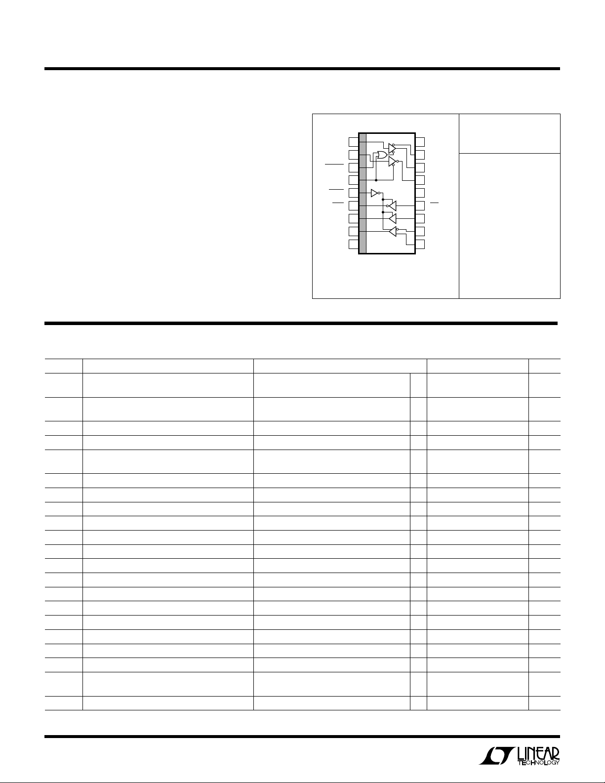
The LTC1320 is an RS422/RS562 line transceiver designed to operate on LocalTalk networks. It provides one
differential RS422 driver, one single-ended RS562 driver,
two single-ended RS562 receivers, and one differential
RS422 receiver. The LTC1320 draws only 1.2mA quiescent current when active and 30µA in shutdown, making
it ideal for use in battery-powered devices and other
systems where power consumption is a primary concern.
The LTC1320 drivers are specified to drive ±2V into 100Ω.
Additionally, the driver outputs three-state when disabled,
during shutdown, or when the power is off; they maintain
high impedance even with output common-mode voltages beyond the power supply rails. Both the driver
outputs and receiver inputs are protected against ESD
damage to beyond 5kV.
The LTC1320 is available in the 18-pin SOL package.
DATA IN
TX ENABLE
RX ENABLE
DATA OUT
SHUTDOWN
A
PPLICATITYPICAL
Typical LocalTalk Connection
5V
1
3
LTC1320
5
8
4
914
18
#1
–5V
22Ω
17
22Ω
16
22Ω
11
22Ω
10
O
22Ω
100pF
22Ω
100pF
22Ω
100pF
22Ω
100pF
U
LocalTalk
TRANSFORMER
1k
1k
LTC1320 • TA01
120Ω
DATA IN
SIGNALS
ON LINE
DATA OUT
(REMOTE
RECEIVER)
Output Waveforms
5V/DIV
2V/DIV
2V/DIV
5V/DIV
50ns/DIV
1
Page 2
LTC1320
WU
U
PACKAGE
/
O
RDER I FOR ATIO
W
O
A
LUTEXI T
S
A
Supply Voltage (VDD)................................................ 7V
Supply Voltage (VSS) .............................................. –7V
Input Voltage (Logic Inputs) ......... –0.3V to VDD + 0.3V
Input Voltage (Receiver Inputs) ............................ ±15V
Driver Output Voltage (Forced) ............................. ±15V
Output Short-Circuit Duration......................... Indefinite
Operating Temperature Range ................... 0°C ot 70°C
Storage Temperature Range ................ –65°c to 150°C
Lead Temperature (Soldering, 10 sec)................ 300°C
DC ELECTRICAL CHARACTERISTICS
SYMBOL PARAMETER CONDITIONS MIN TYP MAX UNITS
V
OD
V
OC
V
OH
V
OL
I
DD
I
SS
Differential Driver Output Voltage No Load ● 8.0 V
Change in Magnitude of Driver RL = 100Ω (Figure 1) 0.2 V
Differential Output Voltage
Driver Common-Mode Output Voltage RL = 100Ω (Figure 1) 3 V
Output Common-Mode Range SD = 5V or Power Off ● ±10 V
Single-Ended Driver Output Voltage No Load ● ±4.0 V
Input High Voltage All Logic Input Pins ● 2.0 V
Input Low Voltage All Logic Input Pins ● 0.8 V
Input Current All Logic Input Pins ● ±1 ±20 µA
Three-State Output Current SD = 5V or Power Off, –10V < VO < 10V ● ±2 ±100 µA
Driver Short-Circuit Current –5V < VO < 5V ● 35 350 500 mA
Receiver Input Resistance – 7V < VIN < 7V ● 12 kΩ
Receiver Output High Voltage IO = –4mA ● 3.5 V
Receiver Output Low Voltage IO = 4mA ● 0.4 V
Receiver Output Short-Circuit Current 0V < VO < 5V ● 785mA
Receiver Output Three-State Current 0V < VO < 5V ● ±2 ±100 µA
Differential Receiver Threshold Voltage –7V < VCM < 7V ● –200 200 mV
Differential Receiver Input Hysteresis –7V < VCM < 7V 70 mV
Single-Ended Receiver Input Low Voltage ● 0.8 V
Single-Ended Receiver Input High Voltage ● 2V
Supply Current No Load, SD = 0V ● 1.2 3.0 mA
Supply Current No Load, SD = 5V ● 2 350 µ A
WUW
ARB
U
G
S
I
TOP VIEW
1
TXD
2
TXI
3
TXDEN
4
SD
5
RXEN
6
RXO
7
RXO
8
RXDO
9
GND
S PACKAGE
18-LEAD PLASTIC SOL
T
= 150°C, θJA = 100°C/W
JMAX
Consult factory for Industrial and Military grade parts.
18
17
16
15
14
13
12
11
10
V
DD
TXD–
+
TXD
TXO
V
SS
RXI
RXI
–
RXD
+
RXD
LTC1320 • PO01
VS = ±5V ±5%, TA = 0°C to 70°C (Notes 2, 3)
RL = 100Ω (Figure 1) ● 2.0 V
RL = 400Ω ● ±3.4 V
No Load, SD = 5V ● 30 350 µA
ORDER PART
NUMBER
LTC1320CS
2
Page 3
LTC1320
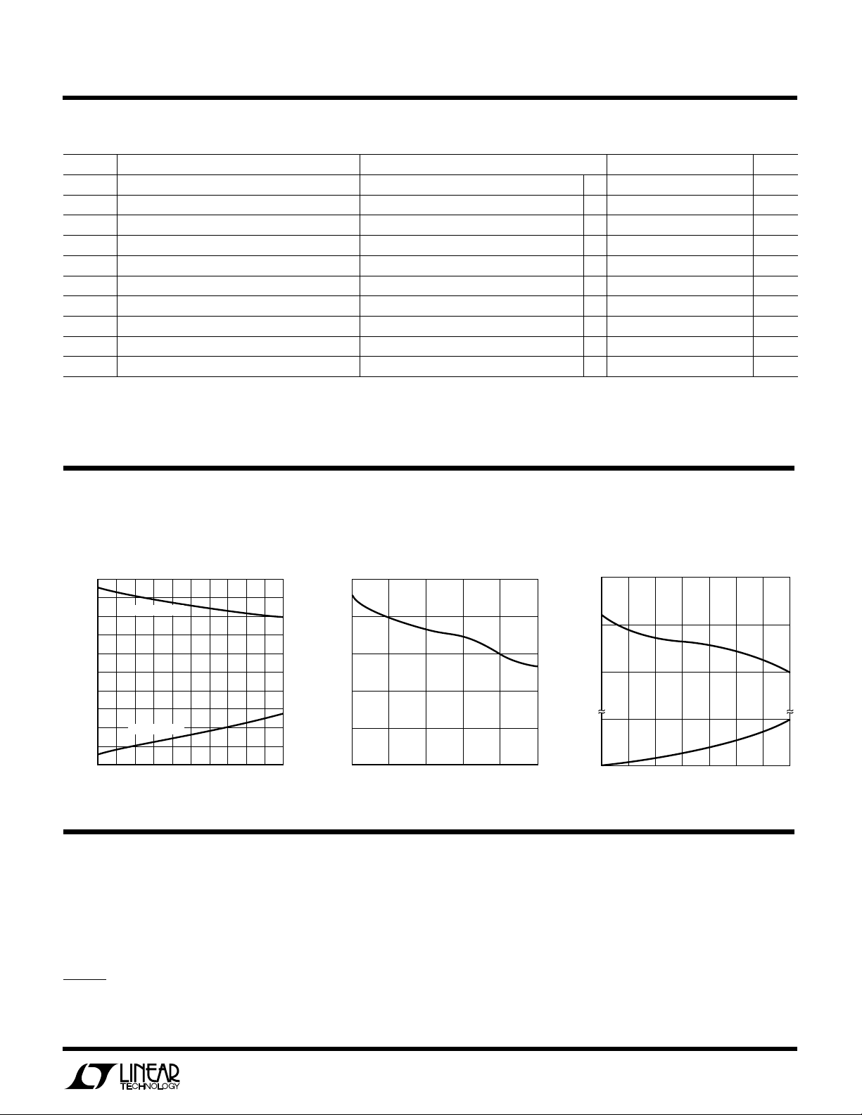
TEMPERATURE (°C)
0
0
SUPPLY CURRENT (mA)
0.004
1.0
1.1
1.2
10 20 30 40
LTC1320 • G03
50 60 70
0.002
I
DD
I
SS
U
SWITCHI G CHARACTERISTICS
SYMBOL PARAMETER CONDITIONS MIN TYP MAX UNITS
t
PLH, HL
t
SKEW
t
r, f
t
ENH, L
t
H, Ldis
t
PLH, HL
t
r, f
t
PLH, HL
t
ENH, L
t
H, Ldis
Differential Driver Propagation Delay RL = 100Ω, CL = 100pF (Figures 2, 8) ● 40 120 ns
Differential Driver Output to Output RL = 100Ω, CL = 100pF (Figures 2, 8) ● 10 50 ns
Differential Driver Rise/Fall Time RL = 100Ω, CL = 100pF (Figures 2, 8) ● 15 80 ns
Driver Enable to Output Active CL = 100pF (Figures 3, 4, 10) ● 50 150 ns
Driver Output Active to Disable CL = 15pF (Figures 3, 4, 10) ● 50 150 ns
Single-Ended Driver Propagation Delay RL = 450Ω, CL = 100pF (Figures 5, 11) ● 40 120 ns
Single-Ended Driver Rise/Fall Time RL = 450Ω, CL = 100pF (Figures 5, 12) ● 15 80 ns
Receiver Propagation Delay CL = 15pF (Figures 13, 14) ● 60 160 ns
Receiver Enable to Output Active CL = 100pF (Figures 6, 7, 15) ● 30 100 ns
Receiver Output Active to Disable CL = 15pF (Figures 6, 7, 15) ● 30 100 ns
VS = ±5V ±5%, TA = 0°C to 70°C (Notes 2, 3)
The ● denotes specifications which apply over the full operating
temperature range.
Note 1: Absolute Maximum Ratings are those values beyond which the life
of a device may be impaired.
UW
LPER
5
4
OUTPUT HIGH
3
2
1
0
–1
OUTPUT SWING (V)
–2
–3
–4
–5
0
OUTPUT LOW
20
R
F
O
60
40
OUTPUT CURRENT (mA)
80
LTC1320 • G01
ATYPICA
100
CCHARA TERIST
E
C
Differential Output Swing vs
Load CurrentOutput Swing vs Load Current
10
8
6
4
2
DIFFERENTIAL OUTPUT SWING (V)
0
20
0
OUTPUT CURRENT (mA)
Note 2: All currents into device pins are positive; all currents out of
device pins are negative. All voltages are referenced to ground unless
otherwise specified.
Note 3: All typicals are given at VS = ±5V, TA = 25°C.
ICS
Supply Current vs Temperature
60
80
40
100
LTC1320 • G02
PI FU CTIO S
TXD (Pin 1): RS422 Differential Driver Input (TTL Compatible).
TXI (Pin 2): RS562 Single-Ended Driver Input (TTL compatible.
TXDEN (Pin 3): RS422 Differential Driver Output Enable
(TTL Compatible). A high level on this pin forces the
U
UU
RS422 driver into three-state; a low level enables the
driver. This input does not affect the RS562 single-ended
driver.
SD (Pin 4): Shutdown Input (TTL Compatible). When this
pin is high, the chip is shut down: all driver outputs threestate and the supply current drops to 30µ A. A low on this
pin allows normal operation.
3
Page 4

LTC1320
OUTPUT
UNDER TEST
C
L
500Ω
V
DD
V
SS
LTC1320 • F03
Figure 3
OUTPUT
UNDER TEST
C
L
LTC1320 • F07
500Ω
Figure 7
U
UU
PI FU CTIO S
RXEN (Pin 5): Receiver Enable (TTL Compatible). A high
level on this pin disables the receivers and three-states the
logic outputs; a low level allows normal operation. To
prevent erratic behavior at the receiver outputs during
shutdown, RXEN should be pulled high along with SD.
RXO (Pin 6): Inverting RS562 Single-Ended Receiver
Output.
RXO (Pin 7): Noninverting RS562 Single-Ended Receiver
Output.
RXDO (Pin 8): RS422 Differential Receiver Output.
GND (Pin 9): Ground Pin.
RXD+ (Pin 10): RS422 Differential Receiver Noninverting
Input. When this pin is ≥200mV above RXD–, RXDO will
be high; when this pin is ≥200mV below RXD–, RXDO will
be low.
RXD– (Pin 11): RS422 Differential Receiver Inverting
Input.
RXI (Pin 12): Noninverting RS562 Receiver Input. This
input controls the RXO output; it has no effect on the RXO
output.
RXI (Pin 13): Inverting RS562 Receiver Input. This input
controls the RXO output; it has no effect on the RXO
output.
V
(Pin 14): Negative Supply. – 4.75 ≥ VSS ≥ –5.25V. The
SS
voltage on this pin must never exceed ground on power up
or power-down.
TXO (Pin 15): RS562 Single-Ended Driver Output.
TXD+ (Pin 16): RS422 Differential Driver Noninverting
Output.
TXD– (Pin 17): RS422 Differential Driver Inverting Output.
V
(Pin 18): Positive Supply. 4.75V ≤ VDD ≤ 5.25V.
DD
TEST CIRCUITS
+
TXD
V
OD
TXD
Figure 1
OUTPUT
UNDER TEST
C
L
V
Figure 4
SS
LTC1320 • F04
RL/2
R
L
500Ω
+
TXD
+
V
/2
OC
–
LTC1320 • F01
TXD
TXD
R
L
–
C
L1
C
L2
LTC1320 • TCF02
Figure 2
R
L
LTC1320 • F05
TXO
500Ω
L
V
LTC1320 • F06
DD
C
L
OUTPUT
UNDER TEST
C
Figure 6
TXI
Figure 5
4
Page 5

LTC1320
U
W
SWITCHI G WAVEFOR S
3V
TXD
0V
–
TXD
+
TXD
V
O
–V
O
TXDEN
TXD+, TXD
TXD+, TXD
–5V
V
V
V
10%
3V
0V
5V
OL
OH
t
r
1.5V
f = 1MHz: t
t
PLH
1.5V
O
1/2 V
O
90%
–
–
< 10ns: tf < 10ns
r
t
SKEW
Figure 8
V
= V(TXD+) – V(TXD–)
DIFF
Figure 9
f = 1MHz: tr ≤ 10ns: tf ≤ 10ns
t
ENL
0V
OUTPUT NORMALLY LOW
OUTPUT NORMALLY HIGH
0V
t
ENH
Figure 10
t
SKEW
1.5V
t
f
t
90%
1.5V
PHL
1/2 V
LTC1320 • F08
10%
LTC1320 • F09
t
Ldis
t
Hdis
O
0.5V
0.5V
LTC1320 • F10
TXI
V
TXO
V
V
OH
V
3V
0V
OH
OL
OL
RXO
RXO
RXI
V
V
RXI
V
V
1.5V
f = 1MHz: t
t
PHL
0V
< 10ns: tf < 10ns
r
1.5V
t
PLH
0V
LTC1320 • F11
Figure 11
10%
90%
t
r
90%
10%
t
f
LTC1320 • F12
Figure 12
3V
0V
OH
OL
3V
0V
OH
OL
1.5V
1.5V
f = 1MHz: t
t
PHL
1.5V
f = 1MHz: t
t
PLH
1.5V
< 10ns: tf < 10ns
r
< 10ns: tf < 10ns
r
1.5V
1.5V
t
t
PLH
1.5V
PHL
1.5V
LTC1320 • F13
Figure 13
2.5V
–
(RXD
) – (RXD+)
–2.5V
V
RXDO
V
RXEN
RXO, RXO, RXDO
RXO, RXO, RXDO
V
V
f = 1MHz: t
0V
t
OH
OL
PHL
1.5V 1.5V
< 10ns: tf < 10ns
r
0V
t
PLH
LTC1320 • F14
Figure 14
3V
0V
5V
OL
OH
0V
f = 1MHz: tr ≤ 10ns: tf ≤ 10ns
1.5V
t
ENL
1.5V
OUTPUT NORMALLY LOW
OUTPUT NORMALLY HIGH
1.5V
t
ENH
t
Hdis
1.5V
t
Ldis
0.5V
0.5V
LTC1320 • F15
Figure 15
5
Page 6

LTC1320
1511
18
0.1µF
5V
914
LTC1320 • TA04
610
138
162
1712
37
41
LTC1320
0.1µF
5
–5V
RS562 OUT
NC
NC
+
–
RS422 OUT
+
–
RS562 IN
RS422 IN
TXO
TXD
+
TXD
–
RXI
RXO
SD
RXEN
TXDEN
RXD
–
RXDO
TXI
RXO
TXD
RXD
+
RXI
V
DD
V
SS
GND
PPLICATI
A
U
O
S
I FOR ATIO
WU
U
Thermal Shutdown Protection
The LTC1320 includes a thermal shutdown circuit which
protects the part against prolonged shorts at the driver
outputs. If any driver output is shorted to another output
or to the power supply, the current will be initially limited
to 450mA max. The die temperature will rise to about
150°C, at which point the thermal shutdown circuit turns
off the driver outputs. When the die cools to about 130°C,
the outputs re-enable. If the shorted condition still exists,
the part will heat again and the cycle will repeat. When the
short is removed, the part will return to normal operation.
This oscillation occurs at about 10Hz and prevents the part
from being damaged by excessive power dissipation.
Power Shutdown
The power shutdown feature of the LTC1320 is designed
primarily for battery-powered systems. When SD (pin 4)
is forced high, the part enters shutdown mode. In shut-
down, the supply current drops from 1.2mA to 30µ A typ.
The driver outputs are three-stated and the power to the
receivers is removed. The receiver outputs are not automatically three-stated in shutdown, and can toggle erroneously due to feedthrough from the inputs. This can be
prevented by pulling RXEN high along with SD; this will
three-state the receiver outputs and prevent the generation of spurious data.
Supply Bypassing
The LTC1320 requires that both VDD and VSS are well
bypassed; data errors can result from inadequate bypassing. Bypass capacitor values of 0.1µ F to 1µF from VDD to
ground and from VSS to ground are adequate. Lead lengths
and trace lengths between the capacitors and the chip
should be short to minimize lead inductance.
U
O
PPLICATITYPICAL
SA
Single 5V Supply RS422 to RS562/RS562 to RS422 Converter
5V
0.1µF
18
171
162
153
134
100µF
+
125
116
107
DRIVER I/O
1N5817
LTC1320 • TA03
8
0.1µF
LTC1320
914
LOGIC I/O
5V
+
+
2µF
2
10µF
4
*LTC1046 GIVES 300µA QUIESCENT
CURRENT WHEN LTC1320 IS SHUT DOWN
LT1054 PROVIDES HIGHER OUTPUT DRIVE
8
LTC1046
LT1054
*
3
5
6
Page 7

LTC1320
171
18
0.1µF
5V
914
LTC1320 • TA06
LTC1320
*GENERAL SEMICONDUCTOR ICTE-22C OR EQUIVALENT
TO OUTSIDE WORLD
PROTECTED AGAINST ESD
DAMAGE TO ±25kV
DATA
INPUT/OUTPUT
0.1µF
–5V
162
153
134
125
116
107
*
*
*
*
*
*
*
TXD
TXI
SD
RXO
TXD
–
TXD
+
TXO
RXI
RXD
–
RXD
+
RXI
TXDEN
RXEN
RXO
8 RXDO
GND V
SS
V
DD
U
O
PPLICATITYPICAL
SA
Switched Negative Supply
5V
TXD
TXI
TXDEN
LOGIC I/O
SD
RXEN
RXO
RXO
8
RXDO
*SCHOTTKY DIODE PREVENTS V
GND ON POWER-UP OR POWER-DOWN
18
LTC1320
914
TXD
TXD
RXD
RXD
–5V
TXO
RXI
RXI
–
+
–
+
0.1µF
171
162
153
134
DRIVER I/O
125
116
107
0.1µF
FROM EXCEEDING
SS
≥25k ESD Protection
1N5817*
LTC1320 • TA05
PACKAGE DESCRIPTIO
S Package
18-Lead Plastic SOL
0.009 – 0.013
(0.229 – 0.330)
NOTE:
PIN 1 IDENT, NOTCH ON TOP AND CAVITIES ON THE BOTTOM OF PACKAGES ARE THE MANUFACTURING OPTIONS.
THE PART MAY BE SUPPLIED WITH OR WITHOUT ANY OF THE OPTIONS.
0.005
(0.127)
RAD MIN
0.291 – 0.299
(7.391 – 7.595)
0.010 – 0.029
(0.254 – 0.737)
SEE NOTE
× 45°
0.016 – 0.050
(0.406 – 1.270)
Information furnished by Linear Technology Corporation is believed to be accurate and reliable.
However, no responsibility is assumed for its use. Linear Technology Corporation makes no representation that the interconnection of circuits as described herein will not infringe on existing patent rights.
U
SEE NOTE
(2.362 – 2.642)
0° – 8° TYP
0.093 – 0.104
0.050
(1.270)
TYP
0.447 – 0.463
(11.354 – 11.760)
14 13
15
1718
16
2345678
1
0.014 – 0.019
(0.356 – 0.482)
TYP
11
12
10
9
0.037 – 0.045
(0.940 – 1.143)
0.004 – 0.012
(0.102 – 0.305)
0.394 – 0.419
(10.007 – 10.643)
SOL18 0392
7
Page 8

LTC1320
U.S. Area Sales Offices
NORTHEAST REGION CENTRAL REGION NORTHWEST REGION
Linear Technology Corporation Linear Technology Corporation Linear Technology Corporation
One Oxford Valley Chesapeake Square 782 Sycamore Dr.
2300 E. Lincoln Hwy.,Suite 306 229 Mitchell Court, Suite A-25 Milpitas, CA 95035
Langhorne, PA 19047 Addison, IL 60101 Phone: (408) 428-2050
Phone: (215) 757-8578 Phone: (708) 620-6910 FAX: (408) 432-6331
FAX: (215) 757-5631 FAX: (708) 620-6977
SOUTHEAST REGION SOUTHWEST REGION
Linear Technology Corporation Linear Technology Corporation
17060 Dallas Parkway 22141 Ventura Blvd.
Suite 208 Suite 206
Dallas, TX 75248 Woodland Hills, CA 91364
Phone: (214) 733-3071 Phone: (818) 703-0835
FAX: (214) 380-5138 FAX: (818) 703-0517
International Sales Offices
FRANCE KOREA TAIWAN
Linear Technology S.A.R.L. Linear Technology Korea Branch Linear Technology Corporation
Immeuble "Le Quartz" Namsong Building, #505 Rm. 801, No. 46, Sec. 2
58 Chemin de la Justice Itaewon-Dong 260-199 Chung Shan N. Rd.
92290 Chatenay Mallabry Yongsan-Ku, Seoul Taipei, Taiwan, R.O.C.
France Korea Phone: 886-2-521-7575
Phone: 33-1-46316161 Phone: 82-2-792-1617 FAX: 886-2-562-2285
FAX: 33-1-46314613 FAX: 82-2-792-1619
GERMANY SINGAPORE UNITED KINGDOM
Linear Techonolgy GMBH Linear Technology Pte. Ltd. Linear Technology (UK) Ltd.
Untere Hauptstr. 9 101 Boon Keng Road The Coliseum, Riverside Way
D-8057 Eching #02-15 Kallang Ind. Estates Camberley, Surrey GU15 3YL
Germany Singapore 1233 United Kingdom
Phone: 49-89-319741-0 Phone: 65-293-5322 Phone: 44-276-677676
FAX: 49-89-3194821 FAX: 65-292-0398 FAX: 44-276-64851
JAPAN
Linear Technology KK
5F YZ Building
4-4-12 Iidabashi Chiyoda-Ku
Tokyo, 102 Japan
Phone: 81-3-3237-7891
FAX: 81-3-3237-8010
World Headquarters
Linear Technology Corporation
1630 McCarthy Blvd.
Milpitas, CA 95035-7487
Phone: (408) 432-1900
FAX: (408) 434-0507
10/92
8
Linear Technology Corporation
1630 McCarthy Blvd., Milpitas, CA 95035-7487
(408) 432-1900
●
FAX
: (408) 434-0507
●
TELEX
: 499-3977
LT/GP 1192 10K REV 0
LINEAR TECHNOLOGY CORPORATION 1992
 Loading...