

Page 1
LTC1292/LTC1297
f
SAMPLE
(Hz)
10
AVERAGE I
CC
(µA)
100
1000
10000
1 100 10k
LTC1297• TA02
1
10
1k 100k
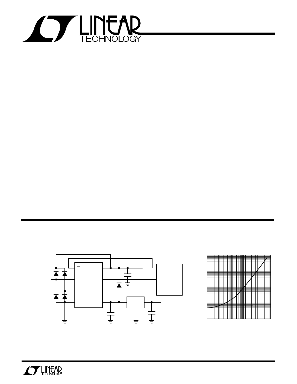
Single Chip 12-Bit
Data Acquisition Systems
EATU
F
■
Built-In Sample-and-Hold
■
Single Supply 5V Operation
■
60kHz Maximum Throughput Rate (LTC1292)
■
Power Shutdown After Each Conversion (LTC1297)
■
Direct 3-Wire Interface to Most MPU Serial Ports and
RE
S
All MPU Parallel Ports
■
Analog Inputs Common Mode to Supply Rails
U
KEY SPECIFICATIO S
■
Resolution: 12 Bits
■
Fast Conversion Time: 12µs Max Over Temp
■
Low Supply Current: 6.0mA
■
Shutdown Supply Current: 5µA (LTC1297)
DUESCRIPTIO
The LTC1292/LTC1297 are data acquisition systems that
contain a 12-bit, switched-capacitor successive approximation A/D, a differential input, sample-and-hold on the
(+) input, and serial I/O. When the LTC1297 is idle between
conversions it automatically powers down reducing the
supply current to 5µA, typically. The LTC1292 is capable
of digitizing signals at a 60kHz rate and with the device’s
excellent AC characteristics, it can be used for DSP applications. All these features are packaged in an 8-pin DIP
and are made possible using LTCMOSTM switched-capacitor technology.
The serial I/O is designed to communicate without external
hardware to most MPU serial ports and all MPU parallel
I/O ports allowing data to be transmitted over three wires.
Because of their accuracy, ease of use and small package
size these devices are well suited for digitizing analog
signals in remote applications where minimum number of
interconnects and power consumption are important.
LTCMOS is trademark of Linear Technology Corporation
DIFFERENTIAL
INPUTS
COMMON MODE
RANGE
0V TO 5V
U
O
A
PPLICATITYPICAL
12-Bit Differential Input Data Acquisition System
LTC1297
V
CC
CLK
1N4148
D
OUT
V
REF
+
AND GND WITH 1N4148 DIODES.
CC
+
4.7µF
TANTALUM
22µF
TANTALUM
LT1027
CS
+
–
*
*FOR OVERVOLTAGE PROTECTION LIMIT THE INPUT CURRENT TO 15mA
PER PIN OR CLAMP THE INPUTS TO V
CONVERSION RESULTS ARE NOT VALID WHEN ANY INPUT IS OVERVOLTAGED
< GND OR V
(V
IN
THE APPLICATIONS INFORMATION.
+IN
–IN
GND
> VCC). SEE SECTION ON OVERVOLTAGE PROTECTION IN
IN
Power Supply Current
vs Sampling Frequency
DO
5V
MC68HC11
SCK
MISO
8V TO 40V
1µF
LTC1292/7 TA01
1
Page 2
LTC1292/LTC1297
O
A
(Notes 1 and 2)
LUTEXI T
S
W
A
WUW
ARB
U
G
I
S
Supply Voltage (VCC) to GND.................................. 12V
Voltage
Analog and Reference
Inputs..................................... –0.3V to V
CC
+ 0.3V
Digital Inputs........................................ –0.3V to 12V
Digital Outputs .......................... –0.3V to V
CC
+ 0.3V
Power Dissipation.............................................. 500mW
Operating Temperature Range
LTC1292/LTC1297BC, LTC1292/LTC1297CC,
LTC1292/LTC1297DC ............................ 0°C to 70°C
LTC1292/LTC1297BI, LTC1292/LTC1297CI,
LTC1292/LTC1297DI ........................ –40°C to 85°C
Storage Temperature Range ................ –65°C to 150°C
Lead Temperature (Soldering, 10 sec.)................ 300°C
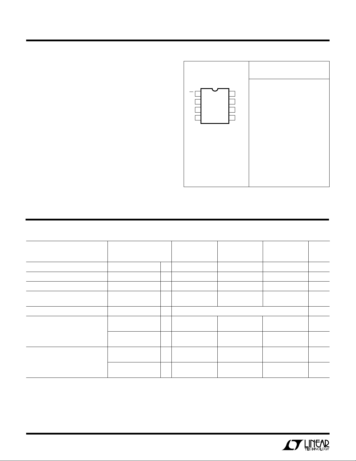
/
PACKAGE
O
RDER I FOR ATIO
ORDER PART NUMBER
TOP VIEW
LTC1292BIN8 LTC1297BIN8
V
CC
LTC1292CIN8 LTC1297CIN8
CLK
LTC1292DIN8 LTC1297DIN8
D
OUT
LTC1292BCJ8 LTC1297BCJ8
V
REF
LTC1292CCJ8 LTC1297CCJ8
LTC1292DCJ8 LTC1297DCJ8
LTC1292BCN8 LTC1297BCN8
LTC1292CCN8 LTC1297CCN8
LTC1292DCN8 LTC1297DCN8
=100°C/W (J8)
JA
=130°C/W (N8)
JA
8
7
6
5
1
CS
2
+IN
3
–IN
4
GND
J8 PACKAGE
8-LEAD CERAMIC DIP
N8 PACKAGE
8-LEAD PLASTIC DIP
T
= 150°C, θ
JMAX
= 100°C, θ
T
JMAX
For Military Temperature Ranges please contact factory.
WU
U
UU W
CO VERTER A D ULTIPLEXER CHARACTERISTICS
LTC1292B
LTC1297B
PARAMETER CONDITIONS MIN TYP MAX MIN TYP MAX MIN TYP MAX UNITS
Offset Error (Note 4) ● ±3.0 ±3.0 ±3.0 LSB
Linearity Error (INL) (Note 4 & 5) ● ±0.5 ±0.5 ±0.75 LSB
Gain Error (Note 4) ● ±0.5 ±1.0 ±4.0 LSB
Minimum Resolution for Which No 12 12 12 Bits
Missing Codes are Guaranteed
Analog and REF Input Range (Note 7) ● –0.05V to VCC + 0.05V V
On Channel Leakage Current On Channel = 5V ● ±1 ±1 ±1 µA
(Note 8) Off Channel = 0V
On Channel = 0V ● ±1 ±1 ±1 µA
Off Channel = 5V
Off Channel Lekage Current On Channel = 5V ● ±1 ±1 ±1 µA
(Note 8) Off Channel = 0V
On Channel = 0V ● ±1 ±1 ±1 µA
Off Channel = 5V
(Note 3)
LTC1292C
LTC1297C
LTC1292D
LTC1297D
2
Page 3
LTC1292/LTC1297
AC CHARACTERISTICS
(Note 3)
LTC1292B/LTC1297B
LTC1292C/LTC1297C
LTC1292D/LTC1297D
SYMBOL PARAMETER CONDITIONS MIN TYP MAX UNITS
f
CLK
t
SMPL
Clock Frequency VCC = 5V (Note 6) (Note 9) 1.0 MHz
Analog Input Sample Time See Operating Sequence LTC1292 1.5CLK
LTC1297 0.5CLK+5.5µs
t
CONV
Conversion Time See Operating Sequence 12 CLK
Cycles
t
CYC
Total Cycle Time See Operating Sequence (Note 6)
LTC1292 14CLK+2.5µs
LTC1297 14CLK+6µs
t
dDO
t
dis
t
en
t
hDO
t
f
t
r
t
WHCLK
t
WLCLK
t
suCS
Delay Time, CLK↓ to D
Delay Time, CS↑ to D
Delay Time, CLK↓ to D
Data Valid See Test Circuits ● 160 300 ns
OUT
Hi-Z See Test Circuits ● 80 150 ns
OUT
Enabled See Test Circuits ● 80 200 ns
OUT
Time Output Data Remains Valid After CLK↓ 130 ns
D
Fall Time See Test Circuits ● 65 130 ns
OUT
D
Rise Time See Test Circuits ● 25 50 ns
OUT
CLK High Time VCC = 5V (Note 6) 300 ns
CLK Low Time VCC = 5V (Note 6) 400 ns
Setup Time, CS↓ Before CLK↑ VCC = 5V (Note 6) LTC1292 50 ns
(LTC1297 Wakeup Time) LTC1297 5.5 µs
t
WHCS
CS High Time Between Data Transfer Cycles VCC = 5V (Note 6) LTC1292 2.5 µs
LTC1297 0.5 µs
t
WLCS
CS Low Time During Data Transfer VCC = 5V (Note 6) LTC1292 14CLK
LTC1297 14CLK+5.5µs
C
IN
Input Capacitance Analog Inputs On Channel 100 pF
Analog Inputs Off Channel 5 pF
Digital Inputs 5 pF
U
DIGITAL A D DC ELECTRICAL CHARACTERISTICS
SYMBOL PARAMETER CONDITIONS MIN TYP MAX UNITS
V
IH
V
IL
I
IH
I
IL
V
OH
V
OL
I
OZ
I
SOURCE
I
SINK
High Level Input Voltage VCC = 5.25V ● 2.0 V
Low Level Input Voltage VCC = 4.75V ● 0.8 V
High Level Input Current VIN = V
CC
Low Level Input Current VIN = 0V ● –2.5 µA
High Level Output Voltage VCC = 4.75V, IO = –10µA 4.7 V
IO = 360µA ● 2.4 4.0 V
Low Level Output Voltage VCC = 4.75V, IO = 1.6mA ● 0.4 V
High Z Output Leakage V
Output Source Current V
Output Sink Current V
= VCC, CS High ● 3 µA
OUT
V
= 0V, CS High ● –3 µA
OUT
= 0V –20 mA
OUT
= V
OUT
CC
(Note 3)
LTC1292B/LTC1297B
LTC1292C/LTC1297C
LTC1292D/LTC1297D
● 2.5 µA
20 mA
3
Page 4
LTC1292/LTC1297
U
DIGITAL A D DC ELECTRICAL CHARACTERISTICS
SYMBOL PARAMETER CONDITIONS MIN TYP MAX UNITS
I
CC
I
REF
The ● denotes specifications which apply over the operating temperature
range; all other limits and typicals T
Note 1: Absolute Maximum Ratings are those values beyond which the life
of a device may be impaired.
Note 2: All voltage values are with respect to ground (unless otherwise
noted).
Note 3: V
Note 4: One LSB is equal to V
= 5V, 1LSB = 5V/4096 = 1.22mV.
Note 5: Linearity error is specified between the actual end points of the
A/D transfer curve. The deviation is measured from the center of the
quantization band.
Note 6: Recommended operating conditions.
Note 7: Two on-chip diodes are tied to each reference and analog input
which will conduct for reference or analog input voltages one diode drop
Positive Supply Current CS High LTC1292 ● 612 mA
CS Low LTC1297 ● 612 mA
CS High
LTC1297BC, LTC1297CC, LTC1297DC ● 510 µA
Power
Shutdown
CLK Off
LTC1297BI, LTC1297CI, LTC1297DI ● 515 µA
LTC1297BM, LTC1297CM, LTC1297DM
Reference Current CS High ● 10 50 µA
below GND or one diode drop above VCC. Be careful during testing at low
= 25°C.
A
levels (4.5V), as high level reference or analog inputs (5V) can cause
V
CC
this input diode to conduct, especially at elevated temperatures, and cause
errors for inputs near full scale. This spec allows 50mV forward bias of
either diode. This means that as long as the reference or analog input does
not exceed the supply voltage by more than 50mV, the output code will be
= 5V, V
CC
= 5V, CLK = 1.0MHz unless otherwise specified.
REF
divided by 4096. For example, when V
REF
correct. To achieve an absolute 0V to 5V input voltage range will therefore
require a minimum supply voltage of 4.950V over initial tolerance,
REF
temperature variations and loading.
Note 8: Channel leakage current is measured after the channel selection.
Note 9: Increased leakage currents at elevated temperatures cause the S/
H to droop, therefore it is recommended that f
≥ 31kHz at 85°C, and f
(Note 3)
≥ 3kHz at 25°C.
CLK
LTC1292B/LTC1297B
LTC1292C/LTC1297C
LTC1292D/LTC1297D
≥125kHz at 125°C, f
CLK
CLK
LPER
10
CLK = 1MHz
= 25°C
T
A
8
6
4
SUPPLY CURRENT (mA)
2
0
4
SUPPLY VOLTAGE (V)
5
F
O
R
ATYPICA
LTC1292/7 G01
UW
CCHARA TERIST
E
C
Supply Current vs TemperatureSupply Current vs Supply Voltage
10
9
8
7
6
5
SUPPLY CURRENT (mA)
4
6
3
–50
–30 –10
ICS
CLK = 1MHz
V
CC
10
AMBIENT TEMPERATURE (°C)
50 90
30 70
= 5V
110
LTC1292/7 G02
130
LTC1297 Supply Current (Power
Shutdown) vs Temperature
10
VCC = 5V
9
= 5V
V
REF
CS HIGH
8
CLK OFF
7
6
5
4
3
SUPPLY CURRENT (µA)
2
1
0
–50
0
–25
AMBIENT TEMPERATURE (°C)
50
25
75
100
LTC1292/7 G03
125
4
Page 5
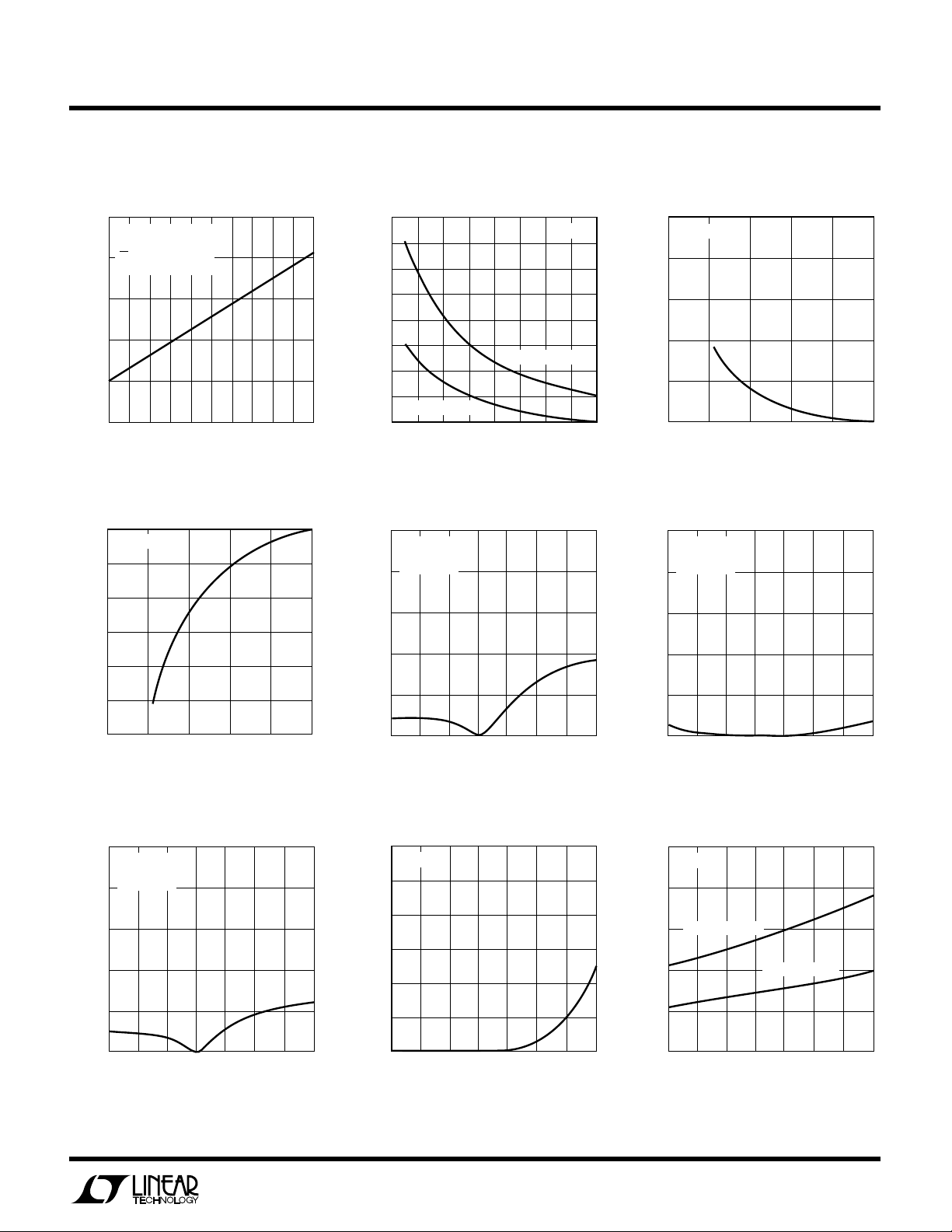
LPER
REFERENCE VOLTAGE (V)
0
LINEARITY (LSB = 1/4096 × V
REF
)
0.75
1.00
1.25
4
LTC1292/7 G06
0.50
0.25
0
1
2
3
5
VCC = 5V
AMBIENT TEMPERATURE (°C)
–50
MAGNITUDE OF LINEARITY CHANGE (LSB)
0.3
0.4
0.5
50
LTC1292/7 G09
0.2
0.1
0
–25
0
25
75
125100
VCC = 5V
V
REF
= 5V
CLK = 1MHz
F
O
R
ATYPICA
UW
CCHARA TERIST
E
C
LTC1292/LTC1297
ICS
LTC1297 Supply Current (Power
Shutdown) vs CLK Frequency
25
VCC = 5V
= 5V
V
REF
CS HIGH
20
CMOS LOGIC LEVELS
15
10
SUPPLY CURRENT (µA)
5
0
200
0
CLK FREQUENCY (kHz)
400
600
800
LTC1292/7 G04
1000
Unadjusted Offset Voltage vs
Reference Voltage
0.9
0.8
)
REF
0.7
0.6
0.5
0.4
0.3
OFFSET (LSB = 1/4096 × V
0.2
V
= 0.125mV
OS
0.1
1
2
REFERENCE VOLTAGE (V)
3
V
OS
Change in Gain vs
Reference Voltage Change in Offset vs Temperature
)
REF
–0.2
–0.4
–0.6
–0.8
0
V
= 5V
CC
0.5
0.4
0.3
0.2
VCC = 5V
= 5V
V
REF
CLK = 1MHz
VCC = 5V
= 0.250mV
4
LTC1292/7 G05
Change in Linearity vs
Reference Voltage
5
Change in Linearity vs
Temperature
–1.0
CHANGE IN GAIN (LSB = 1/4096 × V
–1.2
0
1234
REFERENCE VOLTAGE (V)
Change in Gain vs Temperature
0.5
VCC = 5V
= 5V
V
REF
CLK = 1MHz
0.4
0.3
0.2
0.1
MAGNITUDE OF GAIN CHANGE (LSB)
0
–50
* AS THE CLK FREQUENCY IS DECREASED FROM 1MHz, MINIMUM CLK FREQUENCY (∆ERROR ≤ 0.1LSB) REPRESENTS THE
FREQUENCY AT WHICH A 0.1LSB SHIFT IN ANY CODE TRANSITION FROM ITS 1MHz VALUE IS FIRST DETECTED (NOTE 9).
0
–25
AMBIENT TEMPERATURE (°C)
25
0.1
MAGNITUDE OF OFFSET CHANGE (LSB)
5
LTC1292/7 G07
0
–50
0
–25
AMBIENT TEMPERATURE (°C)
25
50
75
125100
LTC1292/7 G08
Minimum Clock Rate for
D
0.1 LSB Error*
DELAY TIME FROM CLK↓ (ns)
OUT
D
250
200
150
100
VCC = 5V
0.25
0.20
0.15
0.10
0.05
MINIMUM CLK FREQUENCY (MHz)
–50
50
75
125100
LTC1292/7 G10
–25
25
50
0
AMBIENT TEMPERATURE (°C)
75
125100
LTC1292/7 G11
Delay Time vs Temperature
OUT
VCC = 5V
MSB FIRST DATA
LSB FIRST DATA
50
0
–50
–25
25
0
AMBIENT TEMPERATURE (°C)
50
75
125100
LTC1292/7 G12
5
Page 6
LTC1292/LTC1297
R
SOURCE
+ (Ω)
100
1
S & H AQUISITION TIME TO 0.02% (µs)
10
100
1000 10000
LTC1292/7 G15
+
–
+V
IN
R
SOURCE
V
REF
= 5V
V
CC
= 5V
T
A
= 25°C
0V TO 5V INPUT STEP
LPER
F
O
R
ATYPICA
UW
CCHARA TERIST
E
C
ICS
Maximum Clock Rate vs
Source Resistance
1.0
0.8
+V
0.6
0.4
0.2
MAXIMUM CLK FREQUENCY* (MHz)
0
100
1k 10k 100k
R
SOURCE
R
SOURCE
– (Ω)
IN
Input Channel Leakage Current vs
Temperature
1000
900
800
700
600
500
400
300
200
100
INPUT CHANNEL LEAKAGE CURRENT (nA)
0
–30 10
–10
–50
AMBIENT TEMPERATURE (°C)
GUARANTEED
ON CHANNEL
OFF CHANNEL
70 90
50 130
30
VCC = 5V
= 5V
V
REF
CLK = 1MHz
+
+IN
–IN
–
LTC1292/7G13
110
LTC1292/7 G16
Maximum Filter Resistor vs
Cycle Time
10k
R
FILTER
1k
** (Ω)
FILTER
100
10
MAXIMUM R
1
10
+V
C
FILTER
IN
≥1µF
+
–
100
CYCLE TIME (µs)
1k
Noise Error vs Reference Voltage
2.25
LTC1292/LTC1297
2.00
NOISE = 200µV
1.75
1.50
1.25
1.00
0.75
0.50
PEAK-TO-PEAK NOISE ERROR (LSB)
0.25
0
0
P-P
13
2
REFERENCE VOLTAGE (V)
LTC1292/7 G14
4
LTC1292/7 G17
10k
Sample-and-Hold Acquisition
Time vs Source Resistance
* MAXIMUM CLK FREQUENCY REPRESENTS THE
CLK FREQUENCY AT WHICH A 0.1LSB SHIFT IN
THE ERROR AT ANY CODE TRANSITION FROM ITS
1MHz VALUE IS FIRST DETECTED.
** MAXIMUM R
RESISTOR VALUE AT WHICH A 0.1LSB CHANGE IN
FULL SCALE ERROR FROM ITS VALUE AT
R
= 0Ω IS FIRST DETECTED.
FILTER
5
REPRESENTS THE FILTER
FILTER
U
PI FU CTIO S
# PIN FUNCTION DESCRIPTION
1 CS Chip Select Input A logic low on this input enables the LTC1292/LTC1297. Power shutdown is activated on the LTC1297 when
2, 3 +IN, –IN Analog Inputs These inputs must be free of noise with respect to GND.
4 GND Analog Ground GND should be tied directly to an analog ground plane.
5V
6D
7 CLK Shift Clock This clock synchronizes the serial data transfer.
8V
6
REF
OUT
CC
UU
CS is brought high.
Reference Input The reference input defines the span of the A/D converter and must be kept free of noise with respect to GND.
Digital Data Output The A/D conversion result is shifted out of this output.
Positive Supply This supply must be kept free of noise and ripple by bypassing directly to the analog ground plane.
Page 7
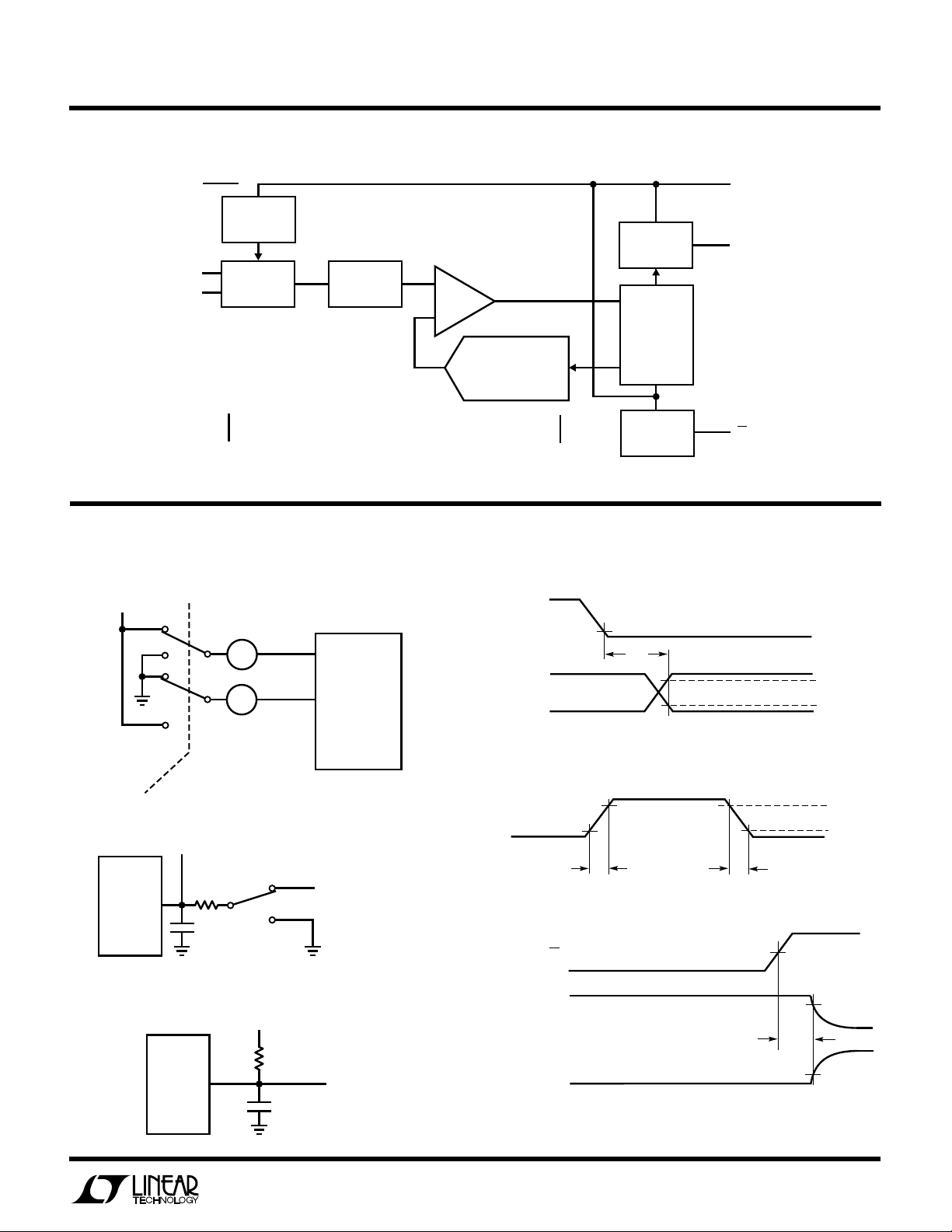
BLOCK
LTC1292/LTC1297
W
IDAGRA
8
V
CC
2
+IN
3
–IN
GND
TEST CIRCUITS
On and Off Channel Leakage Current
5V
INPUT
SHIFT
REGISTER
ANALOG
INPUT MUX
4
I
ON
A
I
OFF
A
SAMPLE
AND
HOLD
ON CHANNEL
OFF CHANNEL
COMP
12-BIT
CAPACITIVE
DAC
CLK
D
OUTPUT
SHIFT
REGISTER
12-BIT
SAR
5
V
REF
CONTROL
AND
TIMING
Voltage Waveforms for D
0.8V
t
dDO
OUT
7
CLK
6
D
OUT
1
CS
LTC1292/7 BD
Delay Time, t
OUT
dDO
2.4V
0.4V
LTC1292/7 TC04
POLARITY
Load Circuit for t
TEST POINT
D
OUT
Load Circuit for t
D
OUT
3k
100pF
1.4V
3kΩ
100pF
dis
dDO
and t
en
5V t
dis
t
WAVEFORM 1
dis
, tr and t
TEST POINT
LTC1292/7 TC01
WAVEFORM 2, t
LTC1292/7 TC02
f
LTC1292/7 TC03
Voltage Waveforms for D
D
OUT
t
r
en
Voltage Waveforms for t
CS
D
OUT
WAVEFORM 1
(SEE NOTE 1)
D
OUT
WAVEFORM 2
(SEE NOTE 2)
NOTE 1: WAVEFORM 1 IS FOR AN OUTPUT WITH INTERNAL CONDITIONS SUCH
THAT THE OUTPUT IS HIGH UNLESS DISABLED BY THE OUTPUT CONTROL.
LTC1292/7 TC06
NOTE 2: WAVEFORM 2 IS FOR AN OUTPUT WITH INTERNAL CONDITIONS SUCH
THAT THE OUTPUT IS LOW UNLESS DISABLED BY THE OUTPUT CONTROL.
Rise and Fall Times, tr, t
OUT
t
f
dis
2.0V
t
dis
f
2.4V
0.4V
LTC1292/7 TC05
90%
10%
7
Page 8
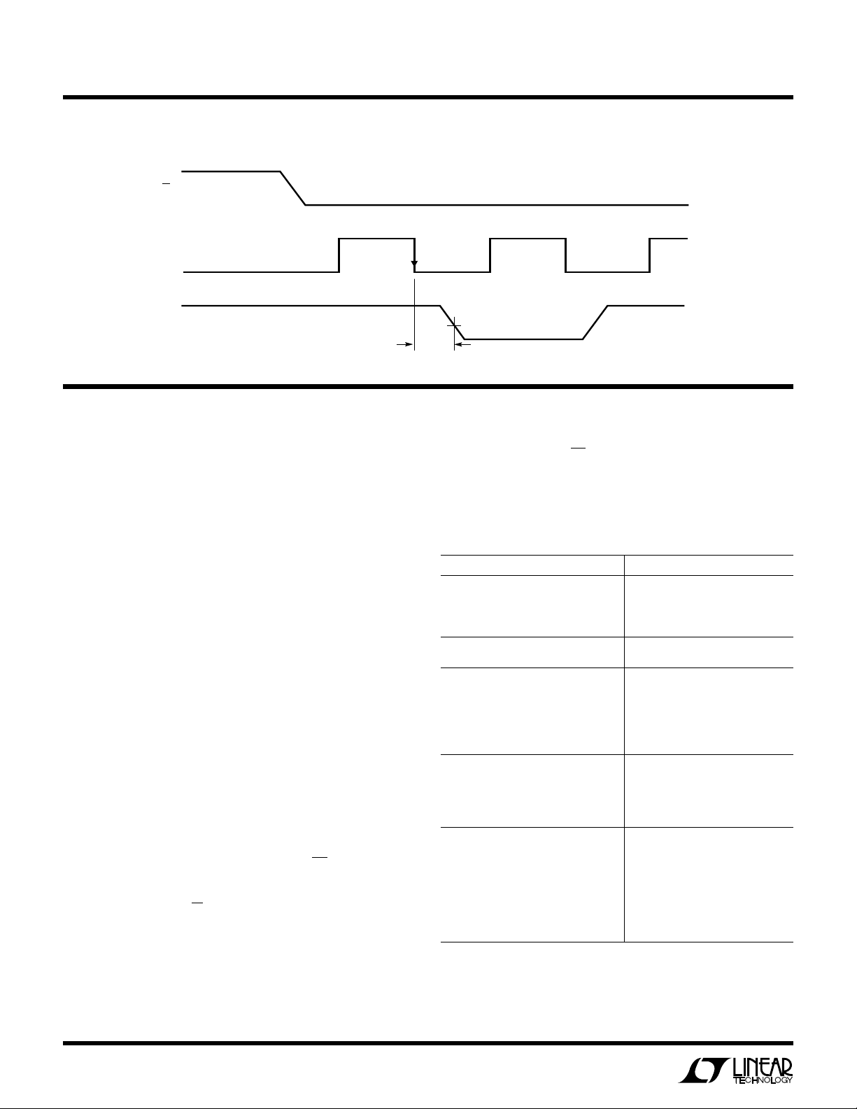
LTC1292/LTC1297
TEST CIRCUITS
Voltage Waveforms for t
CS
CLK
D
OUT
PPLICATI
A
U
O
S
I FOR ATIO
WU
U
The LTC1292/LTC1297 are data acquisition components
which contain the following functional blocks:
1. 12-Bit Succesive Approximation Capacitive A/D
Converter
2. Differential Input
3. Sample-and-Hold (S/H)
4. Synchronous, Half-Duplex Serial Interface
5. Control and Timing Logic
DIGITAL CONSIDERATIONS
Serial Interface
The LTC1292/LTC1297 communicate with microprocessors and other external circuitry via a synchronous, halfduplex, three-wire serial interface (see Operating Sequence). The clock (CLK) synchronizes the data transfer
with each bit being transmitted on the falling CLK edge.
The LTC1292/LTC1297 do not require a configuration
input word and have no DIN pin. They are permanently
configured to have a single differential input and to perform a unipolar conversion. A falling CS initiates data
transfer. To allow the LTC1297 to recover from the power
shutdown mode, t
pulse enables D
OUT
result is output on the D
has to be met. Then the first CLK
suCS
. After one null bit, the A/D conversion
line with a MSB-first sequence
OUT
followed by a LSB-first sequence. With the half-duplex
serial interface the D
data is from the current conver-
OUT
sion. This provides easy interface to MSB-first or LSB-first
en
0.8V
t
en
B11
LTC1292/7 TC07
serial ports. Bringing CS high resets the LTC1292/LTC1297
for the next data exchange and puts the LTC1297 into its
power shutdown mode.
Table 1. Microprocessor with Hardware Serial Interfaces
Compatible with the LTC1292/LTC1297**
PART NUMBER TYPE OF INTERFACE
Motorola
MC6805S2, S3 SPI
MC68HC11 SPI
MC68HC05 SPI
RCA
CDP68HC05 SPI
Hitachi
HD6305 SCI Synchronous
HD6301 SCI Synchronous
HD63701 SCI Synchronous
HD6303 SCI Synchronous
HD64180 SCI Synchronous
National Semiconductor
COP400 Family MICROWIRE
COP800 Family MCROWIRE/PLUS
NS8050U MICROWIRE/PLUS
HPC16000 Family MICROWIRE/PLUS
Texas Instruments
TMS7002 Serial Port
TMS7042 Serial Port
TMS70C02 Serial Port
TMS70C42 Serial Port
TMS32011* Serial Port
TMS32020* Serial Port
TMS370C050 SPI
* Requires external hardware
** Contact factory for interface information for processors not on this list
†
MICROWIRE and MICROWIRE/PLUS are trademarks of National
Semiconductor Corp.
†
†
8
Page 9

LTC1292/LTC1297
PPLICATI
A
CS
CLK
D
OUT
t
SMPL
CS
t
CLK
D
OUT
suCS
t
SMPL
Hi-Z
Hi-Z
B11
U
O
S
I FOR ATIO
B9B10
B11
B7
B8
t
CONV
B9B10
B8
WU
LTC1292 Operating Sequence
B4
B7
t
CONV
B5B6
B3
LTC1297 Operating Sequence
B4
B5B6
U
t
CYC
B3
B0B1B2
B1
t
CYC
B0B1B2
B3
B2
B1
B2
B5B4
B6
B7
B3
B5B4
B6
B7
B10B9B8
B11
POWER SHUTDOWN MODE
B10B9B8
B11
t
SMPL
LTC1292/7 AI01
LTC1292/7 AI02
Microprocessor Interfaces
The LTC1292/LTC1297 can interface directly (without
external hardware) to most popular microprocessors’
(MPU) synchronous serial formats (see Table 1). If an
MPU without a dedicated serial port is used, then three of
the MPU’s parallel port lines can be programmed to form
the serial link to the LTC1292/LTC1297. Included here are
one serial interface example and one example showing a
parallel port programmed to form the serial interface.
CS
CLK
D
OUT
RECEIVED WORD
MPU
B11
BYTE 1
?
?
?
O
1ST TRANSFER
Figure 1. Data Exchange Between LTC1292 and MC68HC11
B10
B10 B9
B9
B8
B8B11
B7
Motorola SPI (MC68HC11)
The MC68HC11 has been chosen as an example of an MPU
with a dedicated serial port. This MPU transfers data MSB
first and in 8-bit increments. A dummy DIN word sent to the
data register starts the SPI process. With two 8-bit transfers,
the A/D result is read into the MPU (Figure 1). For the
LTC1292 the first 8-bit transfer clocks B11 through B8 of
the A/D conversion result into the processor. The second
8-bit transfer clocks the remaining bits B7 through B0 into
B5 B4
B6
B5
B6
B7
B3 B2
BYTE 2
B3B4
2ND TRANSFER
B1
B2 B1
B0
B1
B0
LTC1292/7 F01
9
Page 10

LTC1292/LTC1297
PPLICATI
A
ANALOG
INPUTS
U
O
S
I FOR ATIO
LTC1292
CS
CLK
D
OUT
WU
DO
SCK
MISO
U
MC68HC11
Figure 2. Hardware and Software Interface to Motorola MC68HC11 Microcontroller
MC68HC11 CODE for LTC1292 Interface
LABEL MNEMONIC OPERAND COMMENTS
LDAA #$50 CONFIGURATION DATA FOR SPCR
STAA $1028 LOAD DATA INTO SPCR ($1028)
LDAA #$1B CONFIG. DATA FOR PORT D DDR
STAA $1009 LOAD DATA INTO PORT D DDR
LDAA #$00 LOAD DUMMY DIN WORD INTO
ACC A
STAA $50 LOAD DUMMY DIN DATA INTO $50
LOOP LDX #$1000 LOAD INDEX REGISTER X WITH
$1000
LDAB #$00 LOAD ACC B WITH $00
LDAA $50 LOAD DUMMY DIN INTO ACC A
FROM $50
STAA $102A LOAD DUMMY DIN INTO SPI,
START SCK
NOP DELAY CS FALL TIME TO RIGHT
JUSTIFY DATA
D
FROM LTC1292 STORED ON MC68HC11 RAM
OUT
LOCATION #61
LOCATION #62
LABEL MNEMONIC OPERAND COMMENTS
OO
B5
B6
STAB $08, X D0 GOES LOW (CS GOES LOW)
NOP 6 NOPS FOR TIMING
LDAA $1029 CHECK SPI STATUS REG
LDAA $102A LOAD LTC1292 MSBs INTO ACC A
STAA $61 STORE MSBs IN $61
STAA $102A LOAD DUMMY DIN INTO SPI,
NOPS 6 NOPS FOR TIMING
BSET $08,X,$01 D0 GOES HIGH (CS GOES HIGH)
LDAA $1029 CHECK SPI STATUS REGISTER
LDAA $102A LOAD LTC1292 LSBs IN ACC
STAA $62 STORE LSBs IN $62
JMP LOOP START NEXT CONVERSION
MSB
OO
B4 B2
B10 B9 B8B11
B3B7
B1
B0
START SCK
BYTE 1
BYTE 2
LTC1292/7 F02
the MPU. The data is right-justified in the two memory
locations (Figure 2). This was made possible by delaying
the falling edge of CS till after the second CLK. ANDing the
first byte with 0F
clears the four most significant bits.
HEX
This operation was not included in the code. It can be
inserted in the data gathering loop or outside the loop
when the data is processed.
CS
CLK
D
OUT
RECEIVED WORD
MPU
B11
B11
0
?
B9
B10
BYTE 1
B10
1ST TRANSFER
B8
B8 B7
B6
B7
B6B9
Figure 3. Data Exchange Between LTC1297 and MC68HC11
B5 B4
For the LTC1297 (Figure 3) a delay must be introduced to
accommodate the setup time, t
, before the dummy
suCS
DIN word is sent to the data register. The first 8-bit transfer
clocks B11 through B6 of the A/D conversion result into
the processor. The second 8-bit transfer clocks the remaining bits B5 through B0 into the MPU. Note B1 and B2
from the LSB-first data word have also been clocked in.
B3 B2
BYTE 2
B3
B4
B5
2ND TRANSFER
B0
B1
B1B2
B1
B0 B1
B3
B2
B2
LTC1292/7 F03
10
Page 11

LTC1292/LTC1297
U
O
PPLICATI
A
ANALOG
INPUTS
MC68HC11 CODE for LTC1297 Interface
LABEL MNEMONIC OPERAND COMMENTS
LDAA #$50 CONFIGURATION DATA FOR SPCR
STAA $1028 LOAD DATA INTO SPCR ($1028)
LDAA #$1B CONFIG. DATA FOR PORT D DDR
STAA $1009 LOAD DATA INTO PORT D DDR
LDAA #$00 LOAD DUMMY DIN WORD INTO
STAA $50 LOAD DUMMY DIN DATA INTO $0
LOOP LDX #$1000 LOAD INDEX REGISTER X WITH
LDAB #$00 LOAD ACC B WITH $00
LDAA $50 LOAD DIN INTO ACC FROM $50
BCLR $08,X,$01 D0 GOES LOW (CS GOES LOW)
NOP 3 NOP FOR t
NOP
NOP
STAA $102A LOAD DUMMY DIN INTO SPI,
S
I FOR ATIO
LTC1297
CS
CLK
D
OUT
Figure 4. Hardware and Software Interface to Motorola MC68HC11 Microcontroller
ACC A
$1000
START CLK
WU
DO
SCK
MISO
TIMING
suCS
U
MC68HC11
D
FROM LTC1297 STORED ON MC68HC11 RAM
OUT
LOCATION #61
LOCATION #62
LABEL MNEMONIC OPERAND COMMENTS
LOOP1 LDAA $1029 CHECK SPI STATUS REG
LOOP2 LDAA $1029 CHECK SPI STATUS RES
OO
B5
B6
BPL LOOP1 CHECK IF TRANSFER IS DONE
LDAA $102A LOAD LTC1297 MSBs INTO ACC A
STAA $61 STORE MSBs IN $61
STAA $102A LOAD DUMMY DIN INTO SPI,
BPL LOOP2 CHECK IF TRANSFER IS DONE
BSET $08X,$01 D0 GOES HIGH (CS GOES HIGH)
LDAA $102A LOAD LTC1297 LSBs INTO ACC A
STAA $62 STORE LSBs IN $62
ROR $61 ROTATE RIGHT WITH CARRY
ROR $62 NEEDED TO RIGHT JUSTIFY
ROR $61 THE DATA IN $61 AND $62
ROR $62
JMP LOOP START NEXT CONVERSION
MSB
OO
B4 B2
B10 B9 B8B11
B3B7
B1
B0
START SCK
LTC1292/7 F04
BYTE 1
BYTE 2
The data is right- justified in the two memory locations by
rotating right twice (Figure 4). ANDing the first byte with
0F
clears the four most significant bits. This operation
HEX
was not included in the code. It can be inserted in the data
gathering loop or outside the loop when the data is
processed.
Interfacing to the Parallel Port of the Intel 8051 Family
The Intel 8051 has been chosen to show the interface
between the LTC1292/LTC1297 and parallel port
microprocessors. The signals CS and CLK are generated
on two port lines and the D
signal is read on a third port
OUT
line. After a falling CLK edge each data bit is loaded into the
carry bit and then rotated into the accumulator. Once the
first 8 MSBs have been shifted into the accumulator they
are loaded into register R2. The last four bits are shifted in
the same way and loaded into register R3. The output data
is left-justified in registers R2 and R3 (Figure 5).
For the LTC1297 four NOPs need to be inserted in the 8051
code after CS goes low to allow the LTC1297 to wake up
from power shutdown (t
suCS
).
11
Page 12

LTC1292/LTC1297
PPLICATI
A
O
ANALOG
INPUTS
D
U
S
I FOR ATIO
LTC1292
LTC1297
CS
CLK
OUT
WU
D
CS
CLK
OUT
B11
P1.4
P1.3
P1.1
B10
U
8051
B9
Figure 5. Hardware and Software Interface to Intel 8051 Processor
8051 CODE
LABEL MNEMONIC OPERAND COMMENTS
MOV P1,#02h BIT 1 PORT 1 SET AS INPUT
CLR P1.3 CLK GOES LOW
SETB P1.4 CS GOES HIGH
CONT CLR P1.4 CS GOES LO
NOP 4 NOP FOR LTC1297 t
NOP Time) (Not Needed for LTC1292)
NOP
NOP
SETB P1.3 CLK GOES HIGH
CLR P1.3 CLK GOES LOW
SETB P1.3 CLK GOES HIGH
CLR P1.3 CLK GOES LOW
MOV R4,#08H LOAD COUNTER
LOOP MOV C,P1.1 READ DATA BIT INTO CARRY
RLC A ROTATE DATA BIT INTO ACC
SETB P1.3 CLK GOES HIGH
CLR P1.3 CLK GOES LOW
DJNZ R4,LOOP NEXT BIT
MOV R2,A STORE MSBs IN R2
MOV C,P1.1 READ DATA BIT INTO CARRY
suCS
(Wakeup
D
FROM LTC1292/LTC1297 STORED IN 8051 RAM
OUT
MSB
R2
R3
B8
B7
LABEL MNEMONIC OPERAND COMMENTS
B10 B9 B8B11
B3
B5B6
B1
B2
B3
B4
CLR A CLEAR ACC
RLC A ROTATE DATA BIT (B3) INTO ACC
CLR P1.3 CLK GOES LOW
MOV C,P1.1 READ DATA BIT INTO CARRY
RLC A ROTATE DATA BIT (B2) INTO ACC
SETB P1.3 CLK GOES HIGH
CLR P1.3 CLK GOES LOW
MOV C,P1.1 READ DATA BIT INTO CARRY
RLC A ROTATE DATA BIT (B1) INTO ACC
SETB P1.3 CLK GOES HIGH
CLR P1.3 CLK GOES LOW
MOV C,P1.1 READ DATA BIT INTO CARRY
SETB P1.4 CS GOES HIGH
RRC A ROTATE DATA BIT (B0) INTO ACC
RRC A ROTATE RIGHT INTO ACC
RRC A ROTATE RIGHT INTO ACC
RRC A ROTATE RIGHT INTO ACC
MOV R3,A STORE LSBs IN R3
AJMP CONT START NEXT CONVERSION
B7
B0
OO
B1
B2
SETB P1.3 CLK GOES HIGH
B5
B6
B0
B4
OO
LTC1292/7 F05
Sharing the Serial Interface
The LTC1292/LTC1297 can share the same two-wire
serial interface with other peripheral components or other
LTC1292/LTC1297s (Figure 6). In this case, the CS signals
decide which LTC1292 is being addressed by the MPU.
12
ANALOG CONSIDERATIONS
Grounding
The LTC1292/LTC1297 should be used with an analog
ground plane and single point grounding techniques. Do
not use wire wrapping techniques to breadboard and
evaluate the device. To achieve the optimum performance
Page 13

LTC1292/LTC1297
1
2
3
4
5
6
7
8
22µF
TANTALUM
V
CC
LTC1292/7 F07
LTC1292
LTC1297
0.1µF
U
O
PPLICATI
A
2
10
OUTPUT PORT
SERIAL DATA
MPU
Figure 6. Several LTC1292/LTC1297s Sharing One 2-Wire Serial Interface
2
LTC1292
LTC1297
2 CHANNELS
S
I FOR ATIO
22
CS
LTC1292
LTC1297
2 CHANNELS 2 CHANNELS
use a PC board. The ground pin (Pin 4) should be tied
directly to the ground plane with minimum lead length (a
low profile socket is fine). Figure 7 shows an example of
an ideal LTC1292/LTC1297 ground plane design for a twosided board. Of course this much ground plane will not
always be possible, but users should strive to get as close
to this ideal as possible.
WU
2
LTC1292
LTC1297
CS
CS
U
2-WIRE SERIAL
INTERFACE TO OTHER
PERIPHERALS OR
LTC1292/LTC1297s
LTC1292/7 F06
minimum and the VCC supply should have a low output
impedance such as obtained from a voltage regulator
(e.g., LT323A). For high frequency bypassing a 0.1µF
ceramic disk placed in parallel with the 22µF is
recommended. Again the leads should be kept to a
minimum. Figures 8 and 9 show the effects of good and
poor VCC bypassing.
Figure 7. Example Ground Plane
for the LTC1292/LTC1297
Bypassing
For good performance, V
must be free of noise and
CC
ripple. Any changes in the VCC voltage with respect to
ground during a conversion cycle can induce errors or
noise in the output code. VCC noise and ripple can be kept
below 0.5mV by bypassing the VCC pin directly to the
analog ground plane with a minimum of 22µF tantalum
capacitor and with leads as short as possible. The lead
from the device to the VCC supply also should be kept to a
VERTICAL: 0.5mV/DIV
HORIZONTAL: 10µs/DIV
Analog Inputs
Because of the capacitive redistribution A/D conversion
techniques used, the analog inputs of the LTC1292/
LTC1297 have capacitive switching input current spikes.
These current spikes settle quickly and do not cause a
problem. If large source resistances are used or if slow
settling op amps drive the inputs, take care to insure that
the transients caused by the current spikes settle completely
before the conversion begins.
CS
VERTICAL: 0.5mV/DIV
HORIZONTAL: 10µs/DIV
V
CC
Figure 8. Poor VCC Bypassing. Noise and
Ripple Can Cause A/D Errors
Figure 9. Good VCC Bypassing Keeps
Noise and Ripple on VCC Below 1mV
13
Page 14

LTC1292/LTC1297
PPLICATI
A
U
O
S
I FOR ATIO
WU
U
Source Resistance
The analog inputs of the LTC1292/LTC1297 look like a
100pF capacitor (CIN) in series with a 500Ω resistor (RON)
(Figures 10a and 10b). CIN gets switched between (+) and
(–) inputs once during each conversion cycle. Large
external source resistors and capacitances will slow the
settling of the inputs. It is important that the overall RC
time constant is short enough to allow the analog inputs to
settle completely within the allowed time.
“+” Input Settling
The input capacitor for the LTC1292 is switched onto the
“+” input during the sample phase (t
11b and 11c). The sample period can be as short as t
+ 1/2 CLK cycle or as long as t
WHCS
, see Figures 11a,
SMPL
WHCS
+ 1 1/2 CLK cycles
before a conversion starts. This variability depends on
where CS falls relative to CLK. The voltage on the “+” input
must settle completely within the sample period. Minimizing
R
SOURCE
+ and C1 will improve the settling time. If large “+”
input source resistance must be used, the sample time can
be increased by using a slower CLK frequency. With the
minimum possible sample time of 3.0µ s, R
SOURCE
+ < 2.0k
and C1 < 20pF will provide adequate settling time.
The sample period for the LTC1297 starts on the falling
edge of CS and ends on the falling edge of the first CLK
“+”
INPUT
+
R
VIN +
VIN –
SOURCE
R
SOURCE
CS↑
500Ω
t
WHCS
+ 0.5 CLK
C1
“–”
INPUT
–
C2
LTC1292
RON
CIN
100pF
LTC1292/7 F10a
Figure 10a. Analog Input Equivalent Circuit for the LTC1292
“+”
INPUT
+
R
VIN +
VIN –
SOURCE
R
SOURCE
t
+ 0.5 CLK
CS↓
suCS
500Ω
C1
“–”
INPUT
–
C2
RON
LTC1297
C
IN
100pF
LTC1292/7 F10b
Figure 10b. Analog Input Equivalent Circuit for the LTC1297
(Figure 12). The length of the sample period is t
suCS
+0.5
CLK cycles. Again, the voltage on the “+” input must settle
completely within the sample period. If large “+” input
source resistance must be used, the sample time can be
increased by using a slower CLK frequency or by increasing
14
CLK
D
OUT
(+) INPUT
(–) INPUT
“+” and “–” Input Settling Windows
t
WHCS
CS
t
SUCS
t
(+) INPUT MUST SETTLE DURING THIS TIME
Figure 11a. Setup Time (t
SMPL
HI-Z
1ST BIT TEST (–) INPUT MUST
SETTLE DURING THIS TIME
) Is Met for the LTC1292
suCS
B11
B10
B9
LTC1292/7 F11a
Page 15

LTC1292/LTC1297
PPLICATI
A
CLK
D
OUT
(+) INPUT
(–) INPUT
U
O
S
I FOR ATIO
CS
(+) INPUT MUST SETTLE DURING THIS TIME
WU
t
WHCS
t
SMPL
HI-Z
U
Figure 11b. Setup Time (t
1ST BIT TEST (–) INPUT MUST
SETTLE DURING THIS TIME
) Is Met for the LTC1292
suCS
B11
B10
B9
LTC1292/7 F11b
t
WHCS
CS
CLK
t
(+) INPUT MUST SETTLE DURING THIS TIME
D
OUT
(+) INPUT
(–) INPUT
Figure 11c. Setup Time (t
t
. With the minimum possible sample time of 6µs,
suCS
R
SOURCE
+ < 5k and C1 < 20pF will provide adequate
SMPL
HI-Z
suCS
settling time. In general for both the LTC1292 and LTC1297
keep the product of the total resistance and the total
capacitance less than t
/9. If this condition can not be
SMPL
met, then make C1 > 0.47µF (see RC Input Filtering
section).
1ST BIT TEST (–) INPUT MUST
SETTLE DURING THIS TIME
B11
B10
LTC1292/7 F11c
) Is Not Met for the LTC1292
“–” Input Settling
At the end of the sample phase the input capacitor switches
to the “–” input and the conversion starts (see Figures 11a,
11b, 11c and 12). During the conversion, the “+” input
voltage is effectively “held” by the sample-and-hold and
will not affect the conversion result. It is critical that the
15
Page 16

LTC1292/LTC1297
PPLICATI
A
CS
CLK
D
OUT
(+) INPUT
(–) INPUT
U
O
S
I FOR ATIO
Figure 12. “+” and “–” Input Settling Windows for the LTC1297
WU
t
WHCS
U
(+) INPUT MUST SETTLE
HI-Z
t
suCS
t
SMPL
DURING THIS TIME
1ST BIT TEST (–) INPUT MUST
SETTLE DURING THIS TIME
B11
B10
LTC1292/7 F12
“–” input voltage be free of noise and settle completely
during the first CLK cycle of the conversion. Minimizing
R
SOURCE
– and C2 will improve settling time. If large “–”
input source resistance must be used the time can be
extended by using a slower CLK frequency. At the maximum
CLK frequency of 1MHz, R
SOURCE
– < 250Ω and C2 < 20pF
will provide adequate settling.
Input Op Amps
When driving the analog inputs with an op amp it is
important that the op amp settles within the allowed time
(see Figures 11a, 11b, 11c and 12). Again the “+” and
“–” input sampling times can be extended as described
above to accommodate slower op amps. Most op amps
including the LT1006 and LT1013 single supply op amps
can be made to settle well even with the minimum settling
windows of 3.0µs for the LTC1292 or 6.0µs for the
LTC1297 (“+” input) and 1µ s (“–” input) that occurs at the
maximum clock rate of 1MHz. Figures 13 and 14 show
examples of both adequate and poor op amp settling.
VERTICAL: 5mV/DIV
HORIZONTAL: 500ns/DIV
Figure 13. Adequate Settling of Op Amp Driving Analog Input
VERTICAL: 5mV/DIV
16
HORIZONTAL: 20µs/DIV
Figure 14. Poor Op Amp Settling Can Cause A/D Errors
Page 17

LTC1292/LTC1297
PPLICATI
A
U
O
S
I FOR ATIO
WU
U
RC Input Filtering
It is possible to filter the inputs with an RC network as
shown in Figure 15. For large values of CF (e.g., 1µF) the
capacitive input switching currents are averaged into a net
DC current. A filter should be chosen with a small resistor
and large capacitor to prevent DC drops across the resistor.
The magnitude of the DC current is approximately IDC =
100pF × VIN/t
and is roughly proportional to VIN. When
CYC
running the LTC1292(LTC1297) at the minimum cycle
time of 16.5µs (20µs), the input current equals 30µA
(25µA) at VIN = 5V. Here a filter resistor of 4Ω (5Ω) will
cause 0.1LSB of full scale error. If a large filter resistor
must be used, errors can be reduced by increasing the
cycle time as shown in the typical performance
characteristics curve Maximum Filter Resistor vs Cycle
Time.
I
FILTER
DC
C
FILTER
“+”
LTC1292
LTC1297
“–”
R
V
IN
curve of S&H Acquisition Time vs Source Resistance). The
input voltage is sampled during the t
time as shown
SMPL
in Figure 11. The sampling interval begins at the rising
edge of CS for the LTC1292, and at the falling edge of CS
for the LTC1297, and continues until the falling edge of the
CLK before the conversion begins. On this falling edge the
S&H goes into the hold mode and the conversion begins.
Differential Input
With a differential input the A/D no longer converts a single
voltage but converts the difference between two voltages.
The voltage on the +IN pin is sampled and held and can be
rapidly time-varying as in single-ended mode. The voltage
on the –IN pin must remain constant and be free of noise
and ripple throughout the conversion time. Otherwise the
differencing operation will not be done accurately. The
conversion time is 12 CLK cycles. Therefore a change in
the –IN input voltage during this interval can cause
conversion errors. For a sinusoidal voltage on the –IN
input this error would be:
LTC1292/7 F15
Figure 15. RC Input Filtering
Input Leakage Current
Input leakage currents also can create errors if the source
resistance gets too large. For example, the maximum input
leakage specification of 1µ A (at 125°C) flowing through a
source resistance of 1k will cause a voltage drop of 1mV
or 0.8LSB. This error will be much reduced at lower
temperatures because leakage drops rapidly (see typical
performance characteristics curve Input Channel Leakage
Current vs Temperature).
SAMPLE-AND-HOLD
Single-Ended Input
The LTC1292/LTC1297 provide a built-in sample-andhold (S&H) function on the +IN input for signals acquired
in the single-ended mode (–IN pin grounded). The sampleand-hold allows the LTC1292/LTC1297 to convert rapidly
varying signals (see typical performance characteristics
VfV
ERROR MAX IN PEAK
Where f
V
(–IN)
is its peak amplitude and f
PEAK
CLK. Usually V
=
2
π
( ) (– )
()
is the frequency of the –IN input voltage,
will not be significant. For a 60Hz
ERROR
12
f
CLK
is the frequency of the
CLK
1292/7 E1
signal on the –IN input to generate a 0.25LSB error
(300µV) with the converter running at CLK = 1MHz, its
peak value would have to be 66mV. Rearranging the above
equation the maximum sinusoidal signal that can be
digitized to a given accuracy is given as:
f
IN MAX
(– )
=
ERROR MAX
V
π
2
PEAK
()
f
CLK
12
1292/7 E2
V
For 0.25LSB error (300µV) the maximum input sinusoid
with a 5V peak amplitude that can be digitized is 0.8Hz.
Reference Input
The voltage on the reference input of the LTC1292/
LTC1297 determine the voltage span of the A/D converter. The reference input has transient capacitive
switching currents due to the switched-capacitor con-
17
Page 18

LTC1292/LTC1297
PPLICATI
A
U
O
S
I FOR ATIO
WU
U
version technique (see Figure 16). During each bit test
of the conversion (every CLK cycle) a capacitive current
spike will be generated on the reference pin by the A/D.
These current spikes settle quickly and do not cause a
problem. If slow settling circuitry is used to drive the
reference input, take care to insure that transients
caused by these current spikes settle completely during
each bit test of the conversion.
+
REF
14
V
OUT
REF
–
REF
13
R
Figure 16. Reference Input Equivalent Circuit
EVERY
CLK CYCLE
R
ON
LTC1292
LTC1297
8pF TO 40pF
LTC1292/7 F16
Figures 17 and 18 show examples of both adequate and
poor settling. Using a slower CLK will allow more time
for the reference to settle. Even at the maximum CLK
rate of 1MHz most references and op amps can be
made to settle within the 1µ s bit time. For example the
LT1027 will settle adequately. With a 10µF bypass
capacitor at V
the LT1021 can also be used.
REF
Reduced Reference Operation
The effective resolution of the LTC1292/LTC1297 can
be increased by reducing the input span of the converter. The LTC1292/LTC1297 exhibit good linearity
over a range of reference voltages (see typical performance characteristics curves of Change in Linearity vs
Reference Voltage). Care must be taken when operating at low values of V
because of the reduced LSB
REF
step size and the resulting higher accuracy requirement
placed on the converter. Offset and noise are factors
that must be considered when operating at low V
values. The internal reference for V
has been tied to
REF
REF
the GND pin. Any voltage drop from the GND pin to the
ground plane will cause a gain error.
VERTICAL: 0.5mV/DIV
HORIZONTAL: 1µs/DIV
Figure 17. Adequate Reference Settling (LT1027)
VERTICAL: 0.5mV/DIV
HORIZONTAL: 10µs/DIV
Figure 18. Poor Reference Settling Can Cause A/D Errors
Offset with Reduced V
REF
The offset of the LTC1292/LTC1297 has a larger effect
on the output code when the A/D is operated with a
reduced reference voltage. The offset (which is typically a fixed voltage) becomes a larger fraction of an
LSB as the size of the LSB is reduced. The typical
performance characteristics curve of Unadjusted Offset Error vs Reference Voltage shows how offset in
LSBs is related to reference voltage for a typical value
of VOS. For example a V
of 0.1mV, which is 0.1LSB
OS
with a 5V reference becomes 0.4LSB with a 1.25V
reference. If this offset is unacceptable, it can be
corrected digitally by the receiving system or by offsetting the –IN input to the LTC1292/LTC1297.
Noise with Reduced V
REF
The total input referred noise of the LTC1292/LTC1297
can be reduced to approximately 200µV
using a
P-P
ground plane, good bypassing, good layout techniques
and minimizing noise on the reference inputs. This
noise is insignificant with a 5V reference input but will
18
Page 19

LTC1292/LTC1297
PPLICATI
A
U
O
S
I FOR ATIO
WU
U
become a larger fraction of an LSB as the size of the LSB
is reduced. The typical performance characteristics
curve of Noise Error vs Reference Voltage shows the
LSB contribution of this 200µV of noise.
For operation with a 5V reference, the 200µV noise is
only 0.16LSB peak-to-peak. Here the LTC1292/LTC1297
noise will contribute virtually no uncertainty to the
output code. For reduced references, the noise may
become a significant fraction of an LSB and cause
undesirable jitter in the output code. For example, with
a 1.25V reference, this 200µV noise is 0.64LSB peak-
to-peak. This will reduce the range of input voltages
over which a stable output code can be achieved by
0.64LSB. Now, averaging readings may be necessary.
This noise data was taken in a very clean test fixture.
Any setup induced noise (noise or ripple on VCC, V
REF
or VIN) will add to the internal noise. The lower the
reference voltage used, the more critical it becomes to
have a noise-free setup.
Gain Error Due to Reduced V
REF
The gain error of the LTC1292/LTC1297 is very good
over a wide range of reference voltages. The error
component that is seen in the typical performance
characteristics curve Change in Gain Error vs Reference Voltage is due to the voltage drop on the GND pin
from the device to the ground plane. To minimize this
error the LTC1292/LTC1297 should be soldered directly onto the PC board. The internal reference point
for V
is tied to GND. Any voltage drop in the GND pin
REF
will make the reference voltage, internal to the device,
less than what is applied externally (Figure 19). This
drop is typically 420µV due to the product of the pin
LTC1292
LTC1297
DAC
REF–
REF+
V
GND
ICC
Figure 19. Parasitic Resistance in GND Pin
R
PIN
REF
±
REFERENCE
VOLTAGE
LTC1292/7 F19
resistance (R
current. For example, with V
) and the LTC1292/LTC1297 supply
PIN
= 1.25V this will result
REF
in a gain error change of –1.0LSB from the gain error
measured with V
REF
= 5V.
LTC1292 AC Characteristics
Two commonly used figures of merit for specifying the
dynamic performance of the A/Ds in digital signal
processing applications are the Signal-to-Noise Ratio
(SNR) and the “Effective Number of Bits (ENOB).” SNR
is the ratio of the RMS magnitude of the fundamental to
the RMS magnitude of all the non-fundamental signals
up to the Nyquist frequency (half the sampling frequency). The theoretical maximum SNR for a sine wave
input is given by:
SNR = (6.02N + 1.76dB)
where N is the number of bits. Thus the SNR depends
on the resolution of the A/D. For an ideal 12-bit A/D the
SNR is equal to 74dB. Fast Fourier Transform (FFT)
plots of the output spectrum of the LTC1292 are shown
in Figures 20a and 20b. The input (fIN) frequencies are
1kHz and 28kHz with the sampling frequency (fS) at
58.8 kHz. The SNRs obtained from the plots are 73.0dB
and 61.5dB.
By rewriting the SNR expression it is possible to obtain
the equivalent resolution based on the SNR measurement.
SNR dB
–..176
N
=
602
1292/7 E3
This is the effective number of bits (ENOB). For the
example shown in Figures 20a and 20b, N = 11.8 bits
and 9.9 bits, respectively. Figure 21 shows a plot of
ENOB as a function of input frequency. The 2nd harmonic distortion term accounts for the degradation of
the ENOB as fIN approaches fS/2.
Figure 22 shows an FFT plot of the output spectrum for
two tones applied to the input of the A/D. Nonlinearities
in the A/D will cause distortion products at the sum and
difference frequencies of the fundamentals and products of the fundamentals. This is classically referred to
as intermodulation distortion (IMD).
19
Page 20

LTC1292/LTC1297
U
O
PPLICATI
A
MAGNITUDE (dB)
–20
–40
–60
–80
–100
–120
–140
0
0
S
I FOR ATIO
510
FREQUENCY (kHz)
20 30
15 25
LTC1292/7 F20a
Figure 20a. fIN = 1kHz, fS = 58.8kHz, SNR = 73.0dB
0
–20
–40
–60
–80
MAGNITUDE (dB)
–100
–120
–140
0
510
FREQUENCY (kHz)
20 30
15 25
LTC1292/7 F20b
Figure 20b. fIN = 28kHz, fS = 58.8kHz, SNR = 61.5dB
12.0
11.5
11.0
10.5
10.0
9.5
9.0
EFFECTIVE NUMBER OF BITS
8.5
8.0
20 40 80
0
FREQUENCY (kHz)
fS = 58.8kHz
60
LT1292/7 F21
Figure 21. LTC1292 ENOB vs Input Frequency
WU
100
U
0
–20
–40
–60
–80
MAGNITUDE (dB)
–100
–120
–140
0
Figure 22. f
510
FREQUENCY (kHz)
= 5.1kHz, f
IN1
20 30
15 25
LTC1292/7 F22
= 5.6kHz, fS = 58.8kHz
IN2
Overvoltage Protection
Applying signals to the LTC1292/LTC1297’s analog
inputs that exceed the positive supply or that go below
ground will degrade the accuracy of the A/D and possibly damage the devices. For example this condition
would occur if a signal is applied to the analog inputs
before power is applied to the LTC1292/LTC1297. Another example is the input source is operating from
different supplies of larger value than the LTC1292/
LTC1297. These conditions should be prevented either
with proper supply sequencing or by use of external
circuitry to clamp or current limit the input source.
There are two ways to protect the inputs. In Figure 23
diode clamps from the inputs to VCC and GND are used.
The second method is to put resistors in series with the
analog inputs for current limiting. Limit the current to
15mA per channel. The +IN input can accept a resistor
value of 1k but the –IN input cannot accept more than
250Ω when clocked at its maximum clock frequency of
1MHz. If the LTC1292/LTC1297 are clocked at the
maximum clock frequency and 250Ω is not enough to
current limit the input source, then the clamp diodes are
recommended (Figures 24a and 24b). The reason for
the limit on the resistor value is that the MSB bit test is
affected by the value of the resistor placed at the –IN
input (see discussion on Analog Inputs and the typical
performance characteristics Maximum CLK Frequency
vs Source Resistance).
20
Page 21

LTC1292/LTC1297
U
O
PPLICATI
A
If VCC and V
REF
be turned on first, then V
S
I FOR ATIO
are not tied together, then VCC should
. If this sequence cannot be
REF
met, connecting a diode from V
WU
to VCC is recom-
REF
mended (see Figure 25).
1N4148 DIODES
CS
+IN
LTC1292
LTC1297
–IN
GND
Figure 23. Overvoltage Protection with Clamp Diodes
CS
1k
250Ω
+IN
–IN
GND
LTC1292
LTC1297
Figure 24a. Overvoltage Protection with
Current Limiting Resistors
D
CLK
V
V
OUT
REF
V
CC
CLK
D
OUT
V
REF
5V
CC
LTC1292/7 F24a
5V
LTC1292/7 F23
U
Because a unique input protection structure is used on
the digital input pins, the signal levels on these pins can
exceed the device V
1N4148 DIODES
1k
Figure 24b. Overvoltage Protection with
Diode Clamps and Current Limiting Resistor
Figure 25. Separate VCC and V
without damaging the device.
CC
CS
+IN
–IN
GND
CS
+IN
–IN
GND
LTC1292
LTC1297
LTC1292
LTC1297
V
CC
CLK
D
OUT
V
REF
V
CC
CLK
D
OUT
V
REF
1N4148
LTC1292/7 F25
Supplies
REF
LTC1292/7 F24
5V
5V
5V
V
CLK
+5V
DD
Q4
Q3
Q2
Q1
EN
0.1µF
LTC1292/7 F26
f/32
22µF
CS
V
IN
+IN
LTC1292
–IN
GND
TO OSCILLOSCOPE
V
CC
CLK
D
OUT
V
REF
CLOCK IN
1MHz
CLK
EN
Q1
Q2
Q3
Q4
RESET
V
SS
RESET
CD4520
Figure 26. “Quick Look” Circuit for the LTC1292
21
Page 22

LTC1292/LTC1297
PPLICATI
A
U
O
S
I FOR ATIO
WU
U
A “Quick Look” Circuit for the LTC1292
Users can get a quick look at the function and timing of
the LTC1292 by using the “Quick Look” circuit in Figure
26. V
is tied to VCC. VIN is applied to the +IN input
REF
and the –IN input is tied to the ground plane. CS is driven
at 1/32 the clock rate by the CD4520 and D
the data. The output data from the D
OUT
outputs
OUT
pin can be
viewed on an oscilloscope that is set up to trigger on the
falling edge of CS (Figure 27). Note the LSB data is
partially clocked out before CS goes high.
CLK
CS
D
OUT
A “Quick Look” Circuit for the LTC1297
A circuit similar to the one used for the LTC1292 can be
used for the LTC1297(Figure 28). A one shot has been
generated with NAND gates, a resistor and capacitor to
satisfy the setup time t
. This can be eliminated if a
suCS
slower clock is used. When CS goes low the one shot is
triggered. This turns off the clock to the LTC1297 for a
fixed time to meet t
. Once the clock starts D
suCS
OUT
is
shifted out one bit at a time. CS is driven at 1/64 the
clock rate by the 74HC393. The output data from the
D
pin can be viewed on an oscilloscope that is set to
OUT
trigger on the falling edge of CS. See Figure 29.
CLK
CS
NULL
BIT
MSB
(B11)
VERTICAL: 5V/DIV
HORIZONTAL: 2µs/DIV
LSB
LSB-FIRST DATA
(B0)
(B1)
Figure 27. Scope Trace of the LTC1292 “Quick Look”
Circuit Showing A/D Output 101010101010 (AAA
22µF
TANTALUM
+
CS
V
IN
+IN
LTC1297
–IN
GND
TO OSCILLOSCOPE
D
V
V
CLK
OUT
REF
CC
HEX
f/64
)
D
OUT
LSB-FIRST DATA
LSB
MSB
NULL
(B11)
BIT
VERTICAL: 5V/DIV
HORIZONTAL: 5µs/DIV
(B0)
(B1)
Figure 29. Scope Trace of the LTC1297 “Quick Look”
Circuit Showing A/D Output 101010101010 (AAA
5V
f
A1
CLR1
1QA
1QB
1QC
1QD
GND
74HC393
V
CLR2
2QA
2QB
2QC
2QD
CC
A2
0.1µF
HEX
)
22
340Ω
0.02µF
CLOCK IN 1MHz
Figure 28. “Quick Look” Circuit for the LTC1297
LTC1292/7 F28
Page 23

LTC1292/LTC1297
PPLICATI
A
U
O
S
I FOR ATIO
WU
U
Opto-Isolated Temperature Monitor
Amplification of sensor outputs is often required to
generate a signal large enough to be properly digitized.
For example, a J-type thermocouple provides only
52µV/°C. The 5µV offset of the LTC1050 chopper op
amp generates less than 0.1°C error (Figure 31). Cold
junction compensation is provided by the LT1025A.
(For more detail see LTC Design Note 5).
In the opto-isolated interface two signals are generated
from one. This allows a two-wire interface to the
LTC1292. A long high signal (>1ms) on the CLK IN input
allows the 0.1µ F capacitor to discharge taking CS high.
This resets the A/D for the next conversion. When CLK
IN starts toggling, CS goes low and stays there until the
next extended CLK IN high time. See Figure 30.
ISOLATED
5V
5V/DIV
CLK IN
A
CS
DATA OUT
20µs/DIV
Figure 30. Opto-Isolated Temperature
Monitor Digital Waveforms
+
22 Fµ
2
V
IN
LT1025A
GND
4
2k
0.1%
H
J
–
R
TYPE J
5
0°C – 500°C TEMPERATURE RANGE
3.4k
0.1%
2
–
3
+
+
+
1 F
µ
0.33 Fµ
LTC1050
178k
0.1%
+
7
6
4
47Ω
1 Fµ
1N4148
+
1
2
3
4
LT1019-2.5
LTC1292
CS
+IN
–IN
GND
8
V
CC
7
CLK
6
D
OUT
5
V
REF
4.7 Fµ
3Ω
1N4148
1N4148
A
10k
+
100k
+
0.1 Fµ
74C14
5k
1k
4N28s
3
4
6
500k
1
2
1
5V
1k
2
3
4
6
500k
5V
CLK IN
5k
DATA
OUT
LTC1292/7 F31
Figure 31. Opto-Isolated Temperature Monitor
Information furnished by Linear Technology Corporation is believed to be accurate and reliable.
However, no responsibility is assumed for its use. Linear Technology Corporation makes no representation that the interconnection of its circuits as described herein will not infringe on existing patent rights.
23
Page 24

LTC1292/LTC1297
PACKAGE DESCRIPTIO
U
Dimensions in inches (millimeters) unless otherwise noted.
J8 Package
8-Lead Ceramic DIP
0.290 – 0.320
(7.366 – 8.128)
0.008 – 0.018
(0.203 – 0.457)
0.385 ± 0.025
(9.779 ± 0.635)
0° – 15°
0.300 – 0.320
(7.620 – 8.128)
0.045 – 0.068
(1.143 – 1.727)
FULL LEAD
OPTION
CORNER LEADS OPTION
(4 PLCS)
0.023 – 0.045
(0.584 – 1.143)
HALF LEAD
OPTION
0.200
(5.080)
MAX
0.015 – 0.060
(0.381 – 1.524)
0.045 – 0.068
(1.143 – 1.727)
0.014 – 0.026
(0.360 – 0.660)
NOTE: LEAD DIMENSIONS APPLY TO SOLDER DIP OR TIN PLATE LEADS.
0.100 ± 0.010
(2.540 ± 0.254)
0.125
3.175
MIN
J8 0293
N8 Package
8-Lead Plastic DIP
0.045 – 0.065
(1.143 – 1.651)
0.130 ± 0.005
(3.302 ± 0.127)
0.005
(0.127)
MIN
0.025
(0.635)
RAD TYP
0.400
(10.160)
MAX
876
0.405
(10.287)
MAX
87
12
5
65
3
4
0.220 – 0.310
(5.588 – 7.874)
24
0.065
(1.651)
0.009 – 0.015
(0.229 – 0.381)
+0.025
0.325
–0.015
+0.635
8.255
()
–0.381
TYP
0.045 ± 0.015
(1.143 ± 0.381)
0.100 ± 0.010
(2.540 ± 0.254)
Linear Technology Corporation
1630 McCarthy Blvd., Milpitas, CA 95035-7487
(408) 432-1900
●
FAX
: (408) 434-0507
●
TELEX
: 499-3977
0.125
(3.175)
MIN
0.018 ± 0.003
(0.457 ± 0.076)
0.020
(0.508)
MIN
0.250 ± 0.010
(6.350 ± 0.254)
1234
LT/GP 0294 2K REV A • PRINTED IN USA
LINEAR TECHNOLOGY CORPORATION 1994
N8 0392
 Loading...