

Datasheet LTC1291BIJ8, LTC1291BCN8, LTC1291DMJ8, LTC1291DIN8, LTC1291DIJ8 Datasheet (Linear Technology)
...Page 1
LTC1291
CODE
0
–0.5
DELTA (LSB)
–0.4
–0.2
–0.1
0
0.5
0.2
1024
2048
2560
1291 TA02
–0.3
0.3
0.4
0.1
512 1536
3072
3584
4096
Single Chip 12-Bit
Data Acquisition System
EATU
F
■
Built-In Sample-and-Hold
■
Single Supply 5V Operation
■
Power Shutdown
■
Direct 3- or 4-Wire Interface to Most MPU Serial
RE
S
Ports and All MPU Parallel Ports
■
Two-Channel Analog Multiplexer
■
Analog Inputs Common Mode to Supply Rails
■
8-Pin DIP Package
U
KEY SPECIFICATIO S
■
Resolution: 12 Bits
■
Fast Conversion Time: 12µs Max Over Temp.
■
Low Supply Current:
6.0mA (Typ) Active Mode
10µA (Max) Shutdown Mode
DUESCRIPTIO
The LTC1291 is a data acquisition system that contains a
serial I/O successive approximation A/D converter. It uses
LTCMOSTM switched capacitor technology to perform a
12-bit unipolar A/D conversion. The input multiplexer can
be configured for either single-ended or differential inputs. An on-chip sample-and-hold is included on the “+”
input. When the LTC1291 is idle, it can be powered down
in applications where low power consumption is desired.
An external reference is not required because the LTC1291
takes its reference from the power supply (VCC). All these
features are packaged in an 8-pin DIP.
The serial I/O is designed to communicate without external
hardware to most MPU serial ports and all MPU parallel
I/O ports allowing data to be transmitted over three or four
wires. Given the accuracy, ease of use and small package
size, this device is well suited for digitizing analog signals
in remote applications where minimum number of interconnects, small physical size, and low power consumption are important.
TM
LTCMOS
is a trademark of Linear Technology Corporation
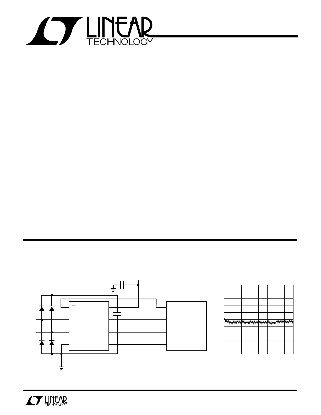
2-CHANNEL
MUX*
U
O
A
PPLICATITYPICAL
2-Channel 12-Bit Data Acquisition System
22µF
TANTALUM
+5V
+
)
LTC1291
V
CC(VREF
D
CLK
OUT
D
0.1µF
IN
AND GND WITH 1N4148 DIODES.
CC
< GND OR V
IN
> VCC). SEE
IN
CS
CH0
CH1
GND
*FOR OVERVOLTAGE PROTECTION LIMIT THE INPUT CURRENT TO 15mA
PER PIN OR CLAMP THE INPUTS TO V
CONVERSION RESULTS ARE NOT VALID WHEN THE SELECTED CHANNEL OR
THE OTHER CHANNEL IS OVERVOLTAGED (V
SECTION ON OVERVOLTAGE PROTECTION IN THE APPLICATIONS INFORMATION.
Channel-to-Channel
INL Matching
DO
SCK
MC68HC11
MISO
MOSI
1291 TA01
1
Page 2
LTC1291
O
A
(Notes 1 and 2)
LUTEXI T
S
W
A
WUW
ARB
U
G
I
S
PACKAGE
/
O
RDER I FOR ATIO
Supply Voltage (VCC) to GND.................................. 12V
Voltage
Analog Inputs............................ –0.3V to V
Digital Inputs........................................ –0.3V to 12V
Digital Outputs .......................... –0.3V to V
Power Dissipation............................................. 500mW
Operating Temperature Range
LTC1291BC, LTC1291CC,
LTC1291DC............................................ 0°C to 70°C
LTC1291BI, LTC1291CI,
LTC1291DI ........................................ –40°C to 85°C
CC
CC
+ 0.3V
+ 0.3V
TOP VIEW
1
CS
2
CH0
3
CH1
45
GND
J8 PACKAGE
8-LEAD CERAMIC DIP
N8 PACKAGE
8-LEAD PLASTIC DIP
LTC1291BM, LTC1291CM,
LTC1291DM................................... –55°C to 125°C
Storage Temperature Range ................ –65°C to 150°C
Lead Temperature (Soldering, 10 sec.)................ 300°C
UU W
CO VERTER A D ULTIPLEXER CHARACTERISTICS
V
CC (VREF
CLK
D
OUT
D
IN
(Note 3)
)
8
7
6
WU
ORDER PART
NUMBER
LTC1291BMJ8
LTC1291CMJ8
LTC1291DMJ8
LTC1291BIJ8
LTC1291CIJ8
LTC1291DIJ8
LTC1291BIN8
LTC1291CIN8
LTC1291DIN8
LTC1291BCN8
LTC1291CCN8
LTC1291DCN8
U
PARAMETER CONDITIONS MIN TYP MAX MIN TYP MAX MIN TYP MAX UNITS
Offset Error (Note 4) ● ±3.0 ±3.0 ±3.0 LSB
Linearity Error (INL) (Note 4 & 5) ● ±0.5 ±0.5 ±0.75 LSB
Gain Error (Note 4) ● ±1.0 ±2.0 ±4.0 LSB
Minimum Resolution for which No
Missing Codes are Guaranteed
Analog Input Range (Note 7) V
On Channel Leakage Current On Channel = 5V
(Note 8) Off Channel = 0V
On Channel = 0V
Off Channel = 5V
Off Channel Lekage Current On Channel = 5V
(Note 8) Off Channel = 0V
On Channel = 0V ● ±1 ±1 ±1 µA
Off Channel = 5V
AC CHARACTERISTICS
SYMBOL PARAMETER CONDITIONS MIN TYP MAX UNITS
f
CLK
t
SMPL
t
CONV
t
CYC
t
dDO
Clock Frequency VCC = 5V (Note 6) (Note 9) 1.0 MHz
Analog Input Sample Time See Operating Sequence 2.5 CLK Cycles
Conversion Time See Operating Sequence 12 CLK Cycles
Total Cycle Time See Operating Sequence (Note 6) 18 CLK Cycles
Delay Time, CLK↓ to D
OUT
(Note 3)
Data Valid See Test Circuits ● 160 300 ns
● 12 12 12 Bits
● ±1 ±1 ±1 µA
● ±1 ±1 ±1 µA
● ±1 ±1 ±1 µA
LTC1291B
LTC1291C
–0.05V to VCC + 0.05V
LTC1291B/LTC1291C/LTC1291D
+ 500ns
LTC1291D
2
Page 3
LTC1291
AC CHARACTERISTICS
SYMBOL PARAMETER CONDITIONS MIN TYP MAX UNITS
t
dis
t
en
t
hDI
t
hDO
t
WHCLK
t
WLCLK
t
f
t
r
t
suDI
t
suCS
t
WHCS
t
WLCS
C
IN
Delay Time, CS↑ to D
Delay Time, CLK↓ to D
Hold Time, DIN after CLK↑ VCC = 5V (Note 6) 50 ns
Time Output Data Remains Valid after CLK↓ 130 ns
CLK High Time VCC = 5V (Note 6) 300 ns
CLK Low Time VCC = 5V (Note 6) 400 ns
D
Fall Time See Test Circuits ● 65 130 ns
OUT
D
Rise Time See Test Circuits ● 25 50 ns
OUT
Setup Time, DIN Stable before CLK↑ VCC = 5V (Note 6) 50 ns
Setup Time, CS↓ before CLK↑ VCC = 5V (Note 6) 50 ns
CS High Time During Conversion VCC = 5V (Note 6) 500 ns
CS Low Time During Data Transfer VCC = 5V (Note 6) 18 CLK Cycles
Input Capacitance Analog Inputs On Channel 100 pF
OUT
OUT
(Note 3)
LTC1291B/LTC1291C/LTC1291D
Hi-Z See Test Circuits ● 80 150 ns
Enabled See Test Circuits ● 80 200 ns
Analog Inputs Off Channel 5 pF
Digital Inputs 5 pF
U
D
DIGITAL
SYMBOL PARAMETER CONDITIONS MIN TYP MAX UNITS
V
IH
V
IL
I
IH
I
IL
V
OH
V
OL
I
OZ
I
SOURCE
I
SINK
I
CC
The
● denotes specifications which apply over the operating temperature
range; all other limits and typicals TA = 25°C.
Note 1: Absolute Maximum Ratings are those values beyond which the life
of a device may be impaired.
Note 2: All voltage values are with respect to ground (unless otherwise
noted).
Note 3: V
Note 4: One LSB is equal to V
5V, 1LSB = 5V/4096 = 1.22mV.
Note 5: Linearity error is specified between the actual end points of the
A/D transfer curve. The deviation is measured from the center of the
quantization band.
Note 6: Recommended operating conditions.
CC
A
High Level Input Voltage VCC = 5.25V ● 2.0 V
Low Level Input Voltage VCC = 4.75V ● 0.8 V
High Level Input Current VIN = V
Low Level Input Current VIN = 0V ● –2.5 µA
High Level Output Voltage VCC = 4.75V, I
Low Level Output Voltage VCC = 4.75V, I
High Z Output Leakage V
Output Source Current V
Output Sink Current V
Positive Supply Current CS High ● 612 mA
= 5V, CLK = 1.0MHz unless otherwise specified.
DC
divided by 4096. For example, when VCC =
CC
LECTRICAL C CHARA TER ST
E
CC
= –10µA 4.7 V
OUT
VCC = 4.75V, I
= VCC, CS High ● 3 µA
OUT
V
= 0V, CS High ● –3 µA
OUT
= 0V –20 mA
OUT
= V
OUT
CS High
Power shutdown
CLK Off
= – 360µA ● 2.4 4.0 V
OUT
= 1.6mA ● 0.4 V
OUT
CC
LTC1291BC, LTC1291CC, LTC1291DC ● 510 µA
LTC1291BI, LTC1291CI, LTC1291DI,
LTC1291BM, LTC1291CM, LTC1291DM
Note 7: Two on-chip diodes are tied to each analog input which will
conduct for analog voltages one diode drop below GND or one diode drop
above VCC. Be careful during testing at low VCC levels (4.5V), as high level
analog inputs (5V) can cause this input diode to conduct, especially at
elevated temperature, and cause errors for inputs near full scale. This spec
allows 50mV forward bias of either diode. This means that as long as the
analog input does not exceed the supply voltage by more than 50mV, the
output code will be correct.
Note 8: Channel leakage current is measured after the channel selection.
Note 9: Increased leakage currents at elevated temperatures cause the
S/H to droop, therefore it is recommended that f
f
CLK
I
≥ 30kHz at 85°C and f
(Note 3)
ICS
LTC1291B/LTC1291C/LTC1291D
● 2.5 µA
20 mA
● 515 µA
≥ 125kHz at 125°C,
≥ 3kHz at 25°C.
CLK
CLK
3
Page 4
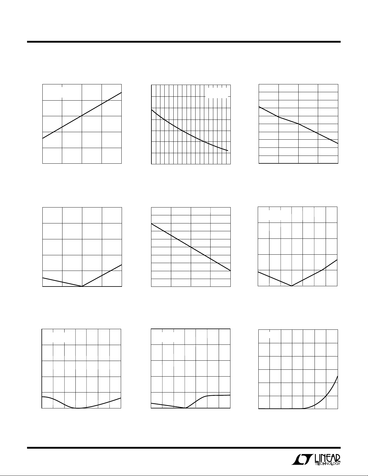
LTC1291
AMBIENT TEMPERATURE (°C)
–50
MINIMUM CLK FREQUENCY* (MHz)
0.15
0.20
0.25
50
1291 G09
0.10
0.05
–25
0
25
75
125100
VCC = 5V
LPER
Supply Current vs Supply Voltage
10
CLK = 1MHz
= 25°C
T
A
8
6
4
SUPPLY CURRENT (mA)
2
0
4
SUPPLY VOLTAGE (V)
F
5
O
R
ATYPICA
6
1291 G01
UW
CCHARA TERIST
E
C
Supply Current vs Temperature
10
9
8
7
6
5
SUPPLY CURRENT (mA)
4
3
–50
–30 –10
AMBIENT TEMPERATURE (°C)
10
ICS
50 90
30 70
CLK = 1MHz
= 5V
V
CC
110
1291 G02
130
Change in Offset vs Supply
Voltage
))
0.5
REF
0.4
(V
CC
0.3
0.2
0.1
0
–0.1
–0.2
–0.3
–0.4
–0.5
CHANGE IN OFFSET (LSB = 1/4096 × V
4.0
4.5
5.0
SUPPLY VOLTAGE (V)
5.5
6.0
1291 G03
Change in Linearity vs Supply
Voltage
))
0.5
REF
(V
CC
0.4
0.3
0.2
0.1
0
CHANGE IN LINEARITY (LSB = 1/4096 × V
4.0
4.5
5.0
SUPPLY VOLTAGE (V)
Change in Linearity vs
Temperature
0.5
VCC = 5V
CLK = 1MHz
0.4
0.3
5.5
1291 G04
6.0
Change in Gain Error vs Supply
Voltage Change in Offset vs Temperature
))
(V
CHANGE IN GAIN ERROR (LSB = 1/4096 × V
REF
CC
–0.1
–0.2
–0.3
–0.4
–0.5
0.5
0.4
0.3
0.2
0.1
0
4.0
4.5
5.0
SUPPLY VOLTAGE (V)
5.5
6.0
1291 G05
0.5
VCC = 5V
CLK = 1MHz
0.4
0.3
0.2
0.1
MAGNITUDE OF OFFSET CHANGE (LSB)
0
–50
0
–25
AMBIENT TEMPERATURE (°C)
50
25
Minimum Clock Rate for
Change in Gain vs Temperature
0.5
VCC = 5V
CLK = 1MHz
0.4
0.3
0.1 LSB Error
100
125
1291 G06
75
0.2
0.1
MAGNITUDE OF LINEARITY CHANGE (LSB)
0
–50
–25
AMBIENT TEMPERATURE (°C)
* AS THE CLK FREQUENCY IS DECREASED FROM 1MHz, MINIMUM CLK FREQUENCY (∆ERROR ≤ 0.1LSB) REPRESENTS THE
FREQUENCY AT WHICH A 0.1LSB SHIFT IN ANY CODE TRANSITION FROM ITS 1MHz VALUE IS FIRST DETECTED.
4
0.2
0.1
MAGNITUDE OF GAIN CHANGE (LSB)
0
0
75
50
25
100
125
1291 G07
–50
0
–25
AMBIENT TEMPERATURE (°C)
50
25
75
100
125
1291 G08
Page 5
LPER
F
O
R
ATYPICA
UW
CCHARA TERIST
E
C
LTC1291
ICS
D
Delay Time vs Temperature
OUT
250
VCC = 5V
200
MSB-FIRST DATA
150
0
LSB-FIRST DATA
25
50
DELAY TIME FROM CLK↓ (ns)
OUT
D
100
50
0
–50
–25
AMBIENT TEMPERATURE (°C)
Sample-and-Hold Acquisition
Time vs Source Resistance
100
VCC = 5V
= 25°C
T
A
0V TO 5V INPUT STEP
R
+
SOURCE
10
S/H AQUISITION TIME TO 0.02% (µs)
1
100
V
IN
+
–
1k 10k
R
+ (Ω)
SOURCE
Maximum Clock Rate vs Source
Resistance
1.0
0.8
0.6
0.4
0.2
MAXIMUM CLK FREQUENCY* (MHz)
75
125100
1291 G10
0
100
1k 10k 100k
R
SOURCE
+V
R
SOURCE
–
(Ω)
VCC = 5V
CLK = 1MHz
IN
–
+
+IN
–IN
–
1291 G11
Maximum Filter Resistor vs
Cycle Time
10k
R
FILTER
1k
** (Ω)
FILTER
100
10
MAXIMUM R
1
10
+V
C
FILTER
IN
≥1µF
+
–
100
CYCLE TIME (µs)
1k
10k
1291 G12
Input Channel Leakage Current
vs Temperature
1000
1291 G13
900
800
700
600
500
400
300
200
100
INPUT CHANNEL LEAKAGE CURRENT (nA)
0
–30 10
–10
–50
AMBIENT TEMPERATURE (°C)
GUARANTEED
ON CHANNEL
OFF CHANNEL
70 90
50 130
30
110
1291 G14
* MAXIMUM CLK FREQUENCY REPRESENTS THE CLK
FREQUENCY AT WHICH A 0.1LSB SHIFT IN THE
ERROR AT ANY CODE TRANSITION FROM ITS 1MHz
VALUE IS FIRST DETECTED.
**MAXIMUM R
VALUE AT WHICH A 0.1LSB CHANGE IN FULL SCALE
ERROR FROM ITS VALUE AT R
DETECTED.
REPRESENTS THE FILTER RESISTOR
FILTER
= 0Ω IS FIRST
FILTER
U
UU
PI FU CTIO S
# PIN FUNCTION DESCRIPTION
1 CS Chip Select Input A logic low on this input enables the LTC1291.
2, 3 CH0, CH1 Analog Inputs These inputs must be free of noise with respect to GND.
4 GND Analog Ground GND should be tied directly to an analog ground plane.
5D
6D
IN
OUT
7 CLK Shift Clock This clock synchronizes the serial data transfer.
8V
CC(VREF
Digital Data Input The multiplexer address is shifted into this input.
Digital Data Output The A/D conversion result is shifted out of this output.
) Positive Supply and This pin provides power and defines the span of the A/D converter. This supply must be kept free of noise and
Reference Voltage ripple by bypassing directly to the analog ground plane.
5
Page 6
LTC1291
D
OUT
WAVEFORM 1
(SEE NOTE 1)
2.0V
t
dis
90%
10%
D
OUT
WAVEFORM 2
(SEE NOTE 2)
CS
NOTE 1: WAVEFORM 1 IS FOR AN OUTPUT WITH INTERNAL CONDITIONS SUCH
THAT THE OUTPUT IS HIGH UNLESS DISABLED BY THE OUTPUT CONTROL.
NOTE 2: WAVEFORM 2 IS FOR AN OUTPUT WITH INTERNAL CONDITIONS SUCH
THAT THE OUTPUT IS LOW UNLESS DISABLED BY THE OUTPUT CONTROL.
1291 TC06
BLOCK
IDAGRA
8
)
V
CC (VREF
W
7
CLK
D
IN
CH0
CH1
TEST CIRCUITS
5
2
3
GND
INPUT
SHIFT
REGISTER
ANALOG
INPUT MUX
4
SAMPLE
AND
HOLD
COMP
12-BIT
CAPACITIVE
DAC
OUTPUT
SHIFT
REGISTER
12-BIT
SAR
CONTROL
AND
TIMING
6
1
1291 BD
D
OUT
CS
Load Circuit for t
1.4V
D
OUT
3k
dDO
100pF
, tr and t
On and Off Channel Leakage Current
5V
I
ON
A
I
OFF
A
POLARITY
6
f
TEST POINT
1291 TC02
ON CHANNEL
OFF CHANNEL
1291 TC01
Load Circuit for t
TEST POINT
D
OUT
3k
100pF
Voltage Waveforms for t
dis
and t
en
5V t
WAVEFORM 2, t
dis
t
WAVEFORM 1
dis
dis
en
1291 TC05
Page 7

TEST CIRCUITS
LTC1291
Voltage Waveforms for D
D
OUT
t
r
CS
D
IN
CLK
D
OUT
Rise and Fall Times, tr, t
OUT
t
f
START
1
2
f
2.4V
0.4V
1291 TC04
CLK
D
OUT
Voltage Waveforms for t
345
Voltage Waveforms for D
0.8V
t
dDO
en
0.8V
Delay Time, t
OUT
B11
dDO
2.4V
0.4V
1291 TC03
PPLICATI
A
U
O
S
I FOR ATIO
WU
U
The LTC1291 is a data acquisition component which
contains the following functional blocks:
1. 12-bit successive approximation capacitive A/D
converter
2. Analog multiplexer (MUX)
3. Sample-and-hold (S/H)
4. Synchronous, half duplex serial interface
5. Control and timing logic
DIGITAL CONSIDERATIONS
Serial Interface
The LTC1291 communicates with microprocessors and
other external circuitry via a synchronous, half duplex,
four-wire serial interface (see Operating Sequence). The
clock (CLK) synchronizes the data transfer with each bit
t
en
1291 TC07
being transmitted on the falling CLK edge and captured on
the rising CLK edge in both transmitting and receiving
systems.
CS
DIN 1
SHIFT MUX
ADDRESS IN
D
OUT
1 NULL
SHIFT A/D CONVERSION
BIT
RESULT OUT
1
DIN 2
D
2
OUT
1291 F01
Figure 1
The input data is first received and then the A/D conversion
result is transmitted (half duplex). Because of the half
duplex operation DIN and D
may be tied together
OUT
allowing transmission over just 3 wires: CS, CLK and
7
Page 8

LTC1291
PPLICATI
A
DATA (DIN/D
U
O
S
I FOR ATIO
). Data transfer is initiated by a falling chip
OUT
WU
U
select (CS) signal. After CS falls the LTC1291 looks for a
start bit. After the start bit is received a 4-bit input word is
shifted into the DIN input which configures the LTC1291
and starts the conversion. After one null bit, the result of
Operating Sequence
(Example: Differential Inputs (CH0+, CH1–))
MSB-FIRST DATA (MSBF = 1)
CS
CLK
START
D
IN
SGL/
DIFF
D
OUT
HI-Z
ODD/
SIGN
MSBF
t
SMPL
PS
B11
t
CONV
t
the conversion appears MSB-first on the D
line. The
OUT
conversion result is output, bit by bit, as the conversion is
performed. At the end of the data exchange CS should be
brought high. This resets the LTC1291 in preparation for
the next data exchange.
CYC
DON'T
CARE
DON'T CARE
B0
B1
FILLED WITH ZEROES
LSB-FIRST DATA (MSBF = 0)
CS
CLK
ODD/
START
SGL/
DIFF
SIGN
D
IN
D
OUT
HI-Z
MSBF
t
SMPL
PS
B11
(Example: Differential Inputs (CH0+, CH1–) and MSB-First Data)
CS
CLK
SGL/
DIFF
ODD/
SIGN
MSBF
HAS BEEN CLOCKED IN
IN
PS
B11
START
D
IN
D
OUT
* STOPPING THE CLOCK WILL HELP REDUCE POWER CONSUMPTION
CS CAN BE BROUGHT HIGH ONCE D
HI-Z
t
CYC
B1
t
CONV
Power Shutdown Operating Sequence
REQUEST POWER SHUTDOWN
DON'T CARE
DATA NOT VALID
DON'T CARE
B0
B0
B1
FILLED WITH
ZEROES
B11
FILLED WITH
SHUTDOWN* NEW CONVERSION BEGINS
START
HI-Z
SGL/
DIFF
ODD/
SIGN
ZEROES
MSBF
DON’T
CARE
PS
1291 AI03
1291 AI04
8
Page 9

LTC1291
PPLICATI
A
U
O
S
I FOR ATIO
WU
U
Input Data Word
The 4-bit data word is clocked into the DIN pin on the rising
edge of the clock after chip select goes low and the start
bit has been recognized. Further inputs on the DIN pin are
then ignored until the next CS cycle. The input word is
defined as follows:
MSB-FIRST/
LSB-FIRST
START
SGL/
DIFF
Figure 2. Input Data Word
ODD/
SIGN
MUX ADDRESS
MSBF
PS
POWER
SHUTDOWN
1291 F02
Start Bit
The first “logical one” clocked into the DIN input after CS
goes low is the start bit. The start bit initiates the data
transfer and all leading zeroes which precede this logical
one will be ignored. After the start bit is received the
remaining bits of the input word will be clocked in. Further
inputs on the DIN pin are then ignored until the next CS
cycle.
MUX Address
The bits of the input word following the START BIT assign
the MUX configuration for the requested conversion. For
a given channel selection, the converter will measure the
voltage between the two channels indicated by the “+” and
“–” signs in the selected row of the following table. In
single-ended mode, all input channels are measured with
respect to GND. Only the “+” inputs have sample-andholds. Signals applied at the “–” inputs must not change
more than the required accuracy during the conversion.
Multiplexer Channel Selection
MUX ADDRESS CHANNEL #
SGL/DIFF ODD/SIGN 0 1 GND
10 + –
11 + –
00 +–
01 –+
MSB-First/LSB-First (MSBF)
The output data of the LTC1291 is programmed for MSBfirst or LSB-first sequence using the MSBF bit. When the
MSBF bit is a logical one, data will appear on the D
OUT
line
in MSB-first format. Logical zeroes will be filled in indefinitely following the last data bit to accommodate longer
word lengths required by some microprocessors. When
the MSBF bit is a logical zero, LSB-first data will follow the
normal MSB-first data on the D
line (see Operating
OUT
Sequence).
Power Shutdown
The power shutdown feature of the LTC1291 is activated
by making the PS bit a logical zero. If CS remains low after
the PS bit has been received, a 12-bit D
word with all
OUT
logical ones will be shifted out followed by logical zeroes
until CS goes high. Then the D
line will go into its high
OUT
impedance state. The LTC1291 will remain in the shutdown mode until the next CS cycle. There is no warm-up
or wait period required after coming out of the power
shutdown cycle so a conversion can commence after CS
goes low (see Power Shutdown Operating Sequence).
9
Page 10

LTC1291
PPLICATI
A
U
O
S
I FOR ATIO
WU
U
Output Code
The LTC1291 performs a unipolar conversion. The following shows the output code and transfer curve:
Unipolar Output Code
1 1 1 1 1 1 1 1 1 1 1 1
OUTPUT CODE
1 1 1 1 1 1 1 1 1 1 1 1
1 1 1 1 1 1 1 1 1 1 1 0
0 0 0 0 0 0 0 0 0 0 0 1
0 0 0 0 0 0 0 0 0 0 0 0
•
•
•
INPUT VOLTAGE
V
– 1LSB
REF
V
– 2LSB
REF
•
•
•
1LSB
0V
INPUT VOLTAGE
= 5V)
(V
REF
4.9988V
4.9976V
•
•
•
0.0012V
0V
1291 AI05a
1 1 1 1 1 1 1 1 1 1 1 0
0 0 0 0 0 0 0 0 0 0 0 1
0 0 0 0 0 0 0 0 0 0 0 0
Microprocessor Interfaces
The LTC1291 can interface directly (without external hardware) to most popular microprocessors’s (MPU) synchronous serial formats (see Table 1). If an MPU without a
dedicated serial port is used, then three of the MPU’s
parallel port lines can be programmed to form the serial
link to the LTC1291. Included here are one serial interface
example and one example showing a parallel port programmed to form the serial interface.
Motorola SPI (MC68HC11)
The MC68HC11 has been chosen as an example of an MPU
with a dedicated serial port. This MPU transfers data MSB
-first and in 8-bit increments. The DIN word sent to the data
register starts the SPI process. With three 8-bit transfers,
the A/D result is read into the MPU. The second 8-bit
transfer clocks B11 through B8 of the A/D conversion
result into the processor. The third 8-bit transfer clocks the
remaining bits, B7 through B0, into the MPU. The data is
right justified in the two memory locations. ANDing the
second byte with 0D
clears the four most significant
HEX
bits. This operation was not included in the code. It can be
inserted in the data gathering loop or outside the loop
when the data is processed.
Unipolar Transfer Curve
•
•
•
V
IN
0V
1LSB
V
REF
–2LSB
V
REF
–1LSB
REF
V
1291 AI05b
Table 1. Microprocessor with Hardware Serial Interfaces
Compatible with the LTC1291**
PART NUMBER TYPE OF INTERFACE
Motorola
MC6805S2, S3 SPI
MC68HC11 SPI
MC68HC05 SPI
RCA
CDP68HC05 SPI
Hitachi
HD6305 SCI Synchronous
HD6301 SCI Synchronous
HD63701 SCI Synchronous
HD6303 SCI Synchronous
HD64180 SCI Synchronous
National Semiconductor
COP400 Family MICROWIRE
COP800 Family MCROWIRE/PLUS
NS8050U MICROWIRE/PLUS
HPC16000 Family MICROWIRE/PLUS
Texas Instruments
TMS7002 Serial Port
TMS7042 Serial Port
TMS70C02 Serial Port
TMS70C42 Serial Port
TMS32011* Serial Port
TMS32020* Serial Port
TMS370C050 SPI
* Requires external hardware
**Contact factory for interface information for processors not on this list
†
MICROWIRE and MICROWIRE/PLUS are trademarks of National
Semiconductor Corp.
†
†
10
Page 11

LTC1291
PPLICATI
A
CS
CLK
D
IN
D
OUT
MPU
TRANSMIT
WORD
MPU
RECEIVED
WORD
U
O
S
000
BYTE 1
BYTE 1
WU
I FOR ATIO
Timing Diagram for Interface to the MC68HC11
SGL/
DIFF
SGL/
DIFF
ODD/
EVEN
ODD/
EVEN
?
START
000
????????
1
U
MSBF PS
PS
MSBF
?
?
X
BYTE 2
0
BYTE 2
B11
DON'T CARE
B3B7 B6 B5 B4 B2 B0B1B11 B10 B9 B8
X
X
B10
X
X
B8
B9
X
B7
X
XX
X
BYTE 3 (DUMMY)
B6
B5 B3
B4
BYTE 3
X
X
B2
B1
X
B0
LTC1291 AI06
Hardware and Software Interface to Motorola MC68HC11
D
FROM LTC1291 STORED IN MC68HC11 RAM
OUT
MSB
#62
#63
0
0
B6
B7 B5
0 B11
0
LSB
B3
B4
B10
B2 B1
B9 B8
BYTE 1
B0
BYTE 2
MC68HC11 CODE
In this example the DIN word configures the input MUX for
a single-ended input to be applied to CH0. The conversion
result is output MSB-first.
LABEL MNEMONIC OPERAND COMMENTS
LDAA #$50 CONFIGURATION DATA FOR SPCR
STAA $1028 LOAD DATA INTO SPCR ($1028)
LDAA #$1B CONFIG. DATA FOR PORT D DDR
STAA $1009 LOAD DATA INTO PORT D DDR
LDAA #$03 LOAD DIN WORD INTO ACC A
STAA $50 LOAD DIN DATA INTO $50
LDAA #$60 LOAD DIN WORD INTO ACC A
STAA $51 LOAD DIN DATA INTO $51
ANALOG
INPUTS
CH0
LTC1291
CH1
D
CLK
OUT
D
CS
IN
D0
SCK
MC68HC11
MISO
MOSI
LTC1291 AI07
LABEL MNEMONIC OPERAND COMMENTS
LDAA #$00 LOAD DUMMY DIN WORD INTO
ACC A
STAA $52 LOAD DUMMY DIN DATA INTO $52
LDX #$1000 LOAD INDEX REGISTER X WITH
$1000
LOOP BCLR $08,X,#$01 D0 GOES LOW (CS GOES LOW)
LDAA $50 LOAD DIN INTO ACC A FROM $50
STAA $102A LOAD DIN INTO SPI, START SCK
11
Page 12

LTC1291
PPLICATI
A
U
O
S
I FOR ATIO
WU
U
LABEL MNEMONIC OPERAND COMMENTS
LDAA $1029 CHECK SPI STATUS REG
WAIT1 BPL WAIT1 CHECK IF TRANSFER IS DONE
LDAA $51 LOAD DIN INTO ACC A FROM $51
STAA $102A LOAD DIN INTO SPI, START SCK
WAIT2 LDAA $1029 CHECK SPI STATUS REG
BPL WAIT2 CHECK IF TRANSFER IS DONE
LDAA $102A LOAD LTC1291 MSBs INTO ACC A
STAA $62 STORE MSBs IN $62
LDAA $52 LOAD DUMMY DIN INTO ACC A
FROM $52
Interfacing to the Parallel Port of the Intel 8051 Family
The Intel 8051 has been chosen to show the interface
between the LTC1291 and parallel port microprocessors.
Usually the signals CS, DIN and CLK are generated on three
port lines and the D
signal is read on a fourth port line.
OUT
Timing Diagram for Interface to Intel 8051
LABEL MNEMONIC OPERAND COMMENTS
STAA $102A LOAD DUMMY DIN INTO SPI,
START SCK
WAIT3 LDAA $1029 CHECK SPI STATUS REG
BPL WAIT3 CHECK IF TRANSFER IS DONE
BSET $08,X#$01 D0 GOES HIGH (CS GOES HIGH)
LDAA $102A LOAD LTC1291 LSBs IN ACC
STAA $63 STORE LSBs IN $63
JMP LOOP START NEXT CONVERSION
This works very well. One can save a line by tying the D
and D
lines together. The 8051 first sends the start bit
OUT
IN
and MUX Address to the LTC1291 over the line connected
to P1.2. Then P1.2 is reconfigured as an input and the 8051
reads back the 12-bit A/D result over the same data line.
(D
IN/DOUT
MSB
B11
R2
R1
CS
13
CLK
DATA
)
D
FROM LTC1291 STORED IN 8051 RAM
OUT
B10
B2
B3 B1
START
8051 P1.2 OUTPUT DATA
8051 P1.2 RECONFIGURED
AS INPUT AFTER THE 5TH RISING
CLK BEFORE THE 5TH FALLING CLK
B8 B7
B9
LSB
B0
PS BIT LATCHED
INTO LTC1291
24
ODD/
SIGN
SGL/
DIFF
TO LTC1291
MSBF
PS
Hardware and Software Interface to Intel 8051
B5 B4
B6
00
0
0
5
B10B9B8
B11
LTC1291 TAKES CONTROL OF DATA
LINE ON 5TH FALLING CLK
ANALOG
INPUTS
B7
B6
B5
LTC1291 SENDS A/D RESULT
BACK TO 8051 P1.2
CH0
LTC1291
CH1
CS
CLK
D
OUT
D
IN
MUX ADDRESS
A/D RESULT
B3 B2
B4
P1.4
P1.3
P1.2
B1
8051
B0
LTC1291 AI08
LTC1291 AI09
12
Page 13

LTC1291
PPLICATI
A
U
O
S
I FOR ATIO
WU
U
8051 Code
In this example the input MUX is configured to accept a
differential input between CH0 and CH1. The result from
the conversion is clocked out MSB-first.
LABEL MNEMONIC OPERAND COMMENTS
SETB P1.4 CS GOES HIGH
CONT MOV A,#98H DIN WORD FOR LTC1291
CLR P1.4 CS GOES LOW
MOV R4,#05H LOAD COUNTER
LOOP1 RLC A ROTATE DIN BIT INTO CARRY
CLR P1.3 CLK GOES LOW
MOV P1.2,C OUTPUT DIN BIT TO LTC1291
SETB P1.3 CLK GOES HIGH
DJNZ R4,LOOP1 NEXT DIN BIT
MOV P1,#04H P1.2 BECOMES AN INPUT
CLR P1.3 CLK GOES LOW
MOV R4,#09H LOAD COUNTER
LOOP MOV C,P1.2 READ DATA BIT INTO CARRY
RLC A ROTATE DATA BIT (B3) INTO ACC
SETB P1.3 CLK GOES HIGH
CLR P1.3 CLK GOES LOW
DJNZ R4,LOOP NEXT DOUT BIT
MOV R2,A STORE MSBS IN R2
MOV C,P1.2 READ DATA BIT INTO CARRY
SETB P1.3 CLK GOES HIGH
LABEL MNEMONIC OPERAND COMMENTS
CLR P1.3 CLK GOES LOW
CLR A CLEAR ACC
RLC A ROTATE DATA BIT (B3) INTO ACC
MOV C,P1.2 READ DATA BIT INTO CARRY
RLC A ROTATE DATA BIT (B2) INTO ACC
SETB P1.3 CLK GOES HIGH
CLR P1.3 CLK GOES LOW
MOV C,P1.2 READ DATA BIT INTO CARRY
RLC A ROTATE DATA BIT (B1) INTO ACC
SETB P1.3 CLK GOES HIGH
CLR P1.3 CLK GOES LOW
MOV C,P1.2 READ DATA BIT INTO CARRY
SETB P1.4 CS GOES HIGH
RRC A ROTATE DATA BIT (B0) INTO ACC
RRC A ROTAGE RIGHT INTO ACC
RRC A ROTAGE RIGHT INTO ACC
RRC A ROTAGE RIGHT INTO ACC
MOV R3,A STORE LSBs IN R3
AJMP CONT START NEXT CONVERSION
Sharing the Serial Interface
The LTC1291 can share the same 3-wire serial interface
with other peripheral components or other LTC1291s
2
10
OUTPUT PORT
SERIAL DATA
MPU
Figure 3. Several LTC1291s Sharing One 3-Wire Serial Interface
3
33
CS
LTC1291
2 CHANNELS
(Figure 3). The CS signals decide which LTC1291 is being
addressed by MPU.
3-WIRE SERIAL
3
CS
LTC1291 LTC1291
2 CHANNELS 2 CHANNELS
INTERFACE TO OTHER
PERIPHERALS OR LTC1291s
CS
LTC1291 F03
13
Page 14

LTC1291
PPLICATI
A
U
O
S
I FOR ATIO
WU
U
ANALOG CONSIDERATIONS
Grounding
The LTC1291 should be used with an analog ground plane
and single point grounding techniques. Do not use wire
wrapping techniques to breadboard and evaluate the device.
To achieve the optimum performance use a PC board. The
ground pin (Pin 4) should be tied directly to the ground
plane with minimum lead length. Figure 4 shows an
example of an ideal LTC1291 ground plane for a two-sided
board. Of course this much ground plane will not always
be possible, but users should strive to get as close to this
ideal as possible.
22µF
TANTALUM
0.1µF
V
CC
VERTICAL: 0.5mV/DIV
HORIZONTAL: 10µs/DIV
Figure 5. Poor VCC Bypassing. Noise and
Ripple Can Cause A/D Errors
CS
1
2
LTC1291
3
ANALOG GROUND
PLANE
Figure 4. Example Ground Plane for the LTC1291
4
8
7
6
5
LTC1291 F04
Bypassing
For good performance, VCC must be free of noise and
ripple. Any changes in the VCC voltage with respect to
ground during the conversion cycle can induce error or
noise in the output code. VCC noise and ripple can be kept
below 0.5mV by bypassing the VCC pin directly to the
analog ground plane with a minimum of 22µF tantalum
capacitor and with leads as short as possible. A 0.1µF
ceramic disk capacitor should also be placed directly
across VCC (Pin 8) and GND (Pin 4) as close to the pins as
possible. The VCC supply should have a low output
impedance such as that obtained from a voltage regulator
(e.g., LT323A). Figures 5 and 6 show the effects of good
and poor VCC bypassing.
V
VERTICAL: 0.5mV/DIV
HORIZONTAL: 10µs/DIV
Figure 6. Good VCC Bypassing Keeps
Noise and Ripple on VCC Below 1mV
CC
Analog Inputs
Because of the capacitive redistribution A/D conversion
techniques used, the analog inputs of the LTC1291 have
capacitive switching input current spikes. These current
spikes settle quickly and do not cause a problem. If large
source resistances are used or if slow settling op amps
drive the inputs, take care to insure the transients caused
by the current spikes settle completely before the
conversion begins.
Minimizing Gain and Offset Error
Because the LTC1291’s reference is taken from the power
supply pin (VCC) proper PC board layout and supply
bypassing is important for attaining the best performance
from the A/D converter. Any parasitic resistance in the V
CC
14
Page 15

LTC1291
PPLICATI
A
U
O
S
I FOR ATIO
WU
U
or GND lead will cause gain errors and offset errors (Figure
7). For the best performance the LTC1291 should be
soldered directly to the PC board. If the source can not be
placed next to the pin and the gain parameter is important
the pin should be Kelvin-sensed to eliminate parasitic
resistances due to long PC traces. For example, 0.1Ω of
resistance in the VCC lead can typically cause 0.5LSB
(ICC × 0.1Ω/VCC) of gain error for VCC = 5V.
When the input MUX is selected for single-ended input the
minus terminal is connected to GND internally on the die.
Any parasitic resistance from the GND pin to the ground
plane will lead to an offset voltage (ICC × RP2).
R
P1
LTC1291
–
+
R
P2
GND
Figure 7. Parasitic Resistance in the VCC and GND Leads
D/A
REF
REF
V
CC
+
–
5V
LTC1291 F07
Source Resistance
The analog inputs of the LTC1291 look like a 100pF
capacitor (CIN) in series with a 500Ω resistor (RON). C
IN
gets switched between “+” and “–” inputs once during
each conversion cycle. Large external source resistors
“+”
VIN +
VIN –
R
SOURCE
R
SOURCE
Figure 8. Analog Input Equivalent Circuit
INPUT
+
3RD CLK↑
R
ON
5TH CLK↓
C1
“–”
INPUT
–
C2
= 500Ω
LTC1291
=
C
IN
100pF
LTC1291 F08
and capacitances will slow the settling of the inputs. It is
important that the overall RC time constant is short
enough to allow the analog inputs to settle completely
within the allowed time.
“+” Input Settling
The input capacitor is switched onto the “+” input during
the sample phase (t
, see Figure 9). The sample period
SMPL
is 2.5 CLK cycles before a conversion starts. The voltage
on the “+” input must settle completely within the sample
period. Minimizing R
SOURCE
+ and C1 will improve the
settling time. If large “+” input source resistance must be
used, the sample time can be increased by using a slower
CLK frequency. With the minimum possible sample time
of 2.5µs, R
SOURCE
+ < 1.0k and C1 < 20pF will provide
adequate settle time.
“–” Input Settling
At the end of the sample phase the input capacitor switches
to the “–” input and the conversion starts (see Figure 9).
During the conversion, the “+” input voltage is effectively
“held” by the sample-and-hold and will not affect the
conversion result. It is critical that the “–” input voltage be
free of noise and settle completely during the first CLK
cycle of the conversion. Minimizing R
SOURCE
– and C2 will
improve settling time. If large “–” input source resistance
must be used, the time can be extended by using a slower
CLK frequency. At the maximum CLK frequency of 1MHz,
R
SOURCE
– < 250Ω and C2 < 20pF will provide adequate
settling.
Input Op Amps
When driving the analog inputs with an op amp it is
important that the op amp settles within the allowed time
(see Figure 9). Again the “+” and “–” input sampling times
can be extended as described above to accommodate
slower op amps. Most op amps including the LT1006 and
LT1013 single supply op amps can be made to settle well
even with the minimum settling windows of 2.5µs (“+”
input) and 1µs (“–” input) that occurs at the maximum
clock rate of 1MHz. Figures 10 and 11 show examples
adequate and poor op amp settling.
15
Page 16

LTC1291
PPLICATI
A
(+) INPUT
(–) INPUT
D
CLK
D
OUT
U
O
S
I FOR ATIO
CS
IN
START
WU
HI-Z
U
SGL/
DIFF
SAMPLE
ODD/
SIGN
“+” INPUT MUST SETTLE DURING THIS TIME
MSBF
t
SMPL
1ST BIT TEST “–” INPUT MUST
SETTLE DURING THIS TIME
HOLD
PS
B11
Figure 9. “+” and “–” Input Settling Windows
VERTICAL: 5mV/DIV
Figure 10. Adequate Settling of Op Amp Driving Analog Input
LTC1291 F09
VERTICAL: 5mV/DIV
HORIZONTAL: 20µs/DIVHORIZONTAL: 500ns/DIV
Figure 11. Poor Op Amp Settling Can Cause A/D Errors
(Note Horizontal Scale)
16
Page 17

LTC1291
PPLICATI
A
U
O
S
I FOR ATIO
WU
U
RC Input Filtering
It is possible to filter the inputs with an RC network as
shown in Figure 12. For large values of CF (e.g., 1µF) the
capacitive input switching currents are averaged into a net
DC current. A filter should be chosen with a small resistor
and a large capacitor to prevent DC drops across the
resistor. The magnitude of the DC current is approximately
IDC = 100pF × VIN/t
and is roughly proportional to VIN.
CYC
When running at the minimum cycle time of 18.5µs, the
input current equals 27µ A at VIN = 5V. Here a filter resistor
of 4.5Ω will cause 0.1LSB of full-scale error. If a large filter
resistor must be used, errors can be reduced by increasing
the cycle time as shown in the typical performance
characteristics curve Maximum Filter Resistor vs Cycle
Time.
I
VIN –
R
FILTER
DC
C
Figure 12. RC Input Filtering
FILTER
“+”
LTC1291
“–”
LTC1291 F12
Input Leakage Current
Input leakage currents also can create errors if the source
resistance gets too large. For example, the maximum input
leakage specification of 1µA (at 125°C) flowing through a
source resistance of 1k will cause a voltage drop of 1mV
or 0.8LSB. This error will be much reduced at lower
temperatures because leakage drops rapidly (see typical
performance characteristics curve Input Channel Leakage
Current vs Temperature).
SAMPLE-AND-HOLD
allows the LTC1291 to convert rapidly varying signals (see
typical performance characteristics curve of S/H Acquisition
Time vs Source Resistance). The input voltage is sampled
during the t
time as shown in Figure 9. The sampling
SMPL
interval begins as the bit preceding the MSBF bit is shifted
in and continues until the falling edge of the PS bit is
received. On this falling edge the S/H goes into the hold
mode and the conversion begins.
Differential Input
With a differential input the A/D no longer converts a single
voltage but converts the difference between two voltages.
The voltage on the +IN pin is sampled and held and can be
rapidly time varying. The voltage on the –IN pin must
remain constant and be free of noise and ripple throughout
the conversion time. Otherwise the differencing operation
will not be done accurately. The conversion time is 12 CLK
cycles. Therefore a change in the –IN input voltage during
this interval can cause conversion errors. For a sinusoidal
voltage on the –IN input this error would be:
V2fV
ERROR MAX IN PEAK
Where f
V
(–IN)
is its peak amplitude and f
PEAK
CLK. Usually V
=
π
() ()
()
−
is the frequency of the –IN input voltage,
will not be significant. For a 60Hz
ERROR
12
f
CLK
is the frequency of the
CLK
signal on the –IN input to generate a 0.25LSB error
(300µV) with the converter running at CLK = 1MHz, its
peak value would have to be 66mV. Rearranging the above
equation the maximum sinusoidal signal that can be
digitized to a given accuracy is given as:
f
IN
()
−
V
=
ERROR MAX
2V
π
PEAK
()
f
CLK
12
For 0.25LSB error (300µV) the maximum input sinusoid
with a 5V peak amplitude that can be digitized is 0.8Hz.
Single-Ended Input
The LTC1291 provides a built-in sample-and-hold (S/H)
function on the +IN input for signals acquired in the singleended mode (–IN pin grounded). The sample-and-hold
17
Page 18

LTC1291
PPLICATI
A
U
O
S
I FOR ATIO
WU
U
Overvoltage Protection
Applying signals to the LTC1291’s analog inputs that
exceed the positive supply or that go below ground will
degrade the accuracy of the A/D and possibly damage the
device. For example this condition would occur if a signal
is applied to the analog inputs before power is applied to
the LTC1291. It can also happen if the input source is
operating from supplies of larger value than the LTC1291
supply. These conditions should be prevented either with
proper supply sequencing or by use of external circuitry to
clamp or current limit the input source.
There are two ways to protect the inputs. In Figure 13 diode
clamps from the inputs to VCC and GND are used. The
second method is to put resistors in series with the analog
inputs for current limiting. Limit the current to 15mA per
channel. The +IN input can accept a resistor value of 1k but
the –IN input cannot accept more than 250Ω when clocked
at its maximum clock frequency of 1MHz. If the LTC1291
is clocked at the maximum clock frequency and 250Ω is
not enough to current limit the input source then the clamp
diodes are recommended (Figures 14 and 15). The reason
for the limit on the resistor value is the MSB bit test is
affected by the value of the resistor placed at the –IN input
(see discussion on Analog Inputs and the typical performance characteristics Maximum CLK Frequency vs Source
Resistance).
Because a unique input protection structure is used on the
digital input pins, the signal levels on these pins can
exceed the device VCC without damaging the device.
1N4148 DIODES
CS
CH0
CH1
GND
V
CC (VREF
LTC1291
D
CLK
OUT
D
)
IN
5V
LTC1291 F13
Figure 13. Overvoltage Protection for Inputs
5V
)
IN
LTC1291 F14
1k
250Ω
CS
CH0
CH1
GND
V
CC (VREF
LTC1291
CLK
D
OUT
D
Figure 14. Overvoltage Protection for Inputs
1N4148 DIODES
CS
V
)
CC (VREF
1k
CH0
CH1
GND
LTC1291
D
CLK
OUT
D
IN
5V
LTC1291 F15
18
Figure 15. Overvoltage Protection for Inputs
Page 19

LTC1291
PPLICATI
A
U
O
S
I FOR ATIO
WU
U
A “Quick Look” Circuit for the LTC1291
Users can get a quick look at the function and timing of
the LTC1291 by using the following simple circuit
(Figure 16). DIN is tied to VCC. This requires VIN be
applied to CH1 with respect to the ground plane. The
22µF TANTALUM
+
CS
VCC (V
)
REF
CH0
V
IN
CH1
GND
TO OSCILLOSCOPE
LTC1291
CLK
D
OUT
D
0.1µF
IN
data is output MSB-first. CS is driven at 1/64 the clock
frequency by the 74HC393 and D
The output data from the D
OUT
outputs the data.
OUT
pin can be viewed on a
oscilloscope that is set up to trigger on the falling edge
of CS (Figure 17).
5V
f/64
A1
f
CLR1
1QA
1QB
74HC393
1QC
1QD
GND
CLOCK IN 1MHz
V
CLR2
2QA
2QB
2QC
2QD
CC
A2
0.1µF
LTC1291 F16
Figure 16. “Quick Look” Circuit for the LTC1291
CLK
CS
D
OUT
NULL
BIT
MSB
(B11)
VERTICAL: 5V/DIV
HORIZONTAL: 5µs/DIV
LSB
(B0)
FILLS WITH
ZEROES
Figure 17. Scope Trace of the LTC1291 "Quick Look"
Circuit Showing Output 101010101010 (AAA
HEX
)
Information furnished by Linear Technology Corporation is believed to be accurate and reliable.
However, no responsibility is assumed for its use. Linear Technology Corporation makes no representation that the interconnection of its circuits as described herein will not infringe on existing patent rights.
19
Page 20

LTC1291
PACKAGE DESCRIPTIO
0.290 – 0.320
(7.37 – 8.13)
0.008 – 0.018
(0.203 – 0.460)
0.385 ± 0.025
(9.779 ± 0.635)
0° – 15°
0.014 – 0.026
(0.360 – 0.660)
0.038 – 0.068
(0.965 – 1.727)
U
Dimensions in inches (millimeters) unless otherwise noted.
J8 Package
8-Lead Ceramic DIP
0.005
(0.127)
0.015 – 0.060
(0.381 – 1.524)
0.100 ± 0.010
(2.540 ± 0.254)
0.200
(5.080)
MAX
0.125
3.175
MIN
0.025
(0.635)
RAD TIP
0.055
(1.397)
MAX
MIN
8
1 2
(10.287)
7
0.405
MAX
6 5
3 4
0.220 – 0.310
(5.588 – 7.874)
0.300 – 0.320
(7.620 – 8.128)
+0.025
0.325
–0.015
+0.635
(
8.255
–0.381
T
JMAX
150°C 100°C/W
θ
JA
N8 Package
8-Lead Plastic DIP
0.400
(10.160)
8
1 2
MAX
7 6
5
0.250 ± 0.010
(6.350 ± 0.254)
3
4
0.045 – 0.065
0.065
(1.651)
TYP
0.009 – 0.015
(0.229 – 0.381)
)
(1.143 – 1.651)
0.045 ± 0.015
(1.143 ± 0.381)
0.100 ± 0.010
(2.540 ± 0.254)
T
JMAXθJA
100°C 130°C/W
0.130 ± 0.005
(3.302 ± 0.127)
0.125
(3.175)
0.018 ± 0.003
(0.457 ± 0.076)
0.020
(0.508)
MIN
MIN
20
Linear Technology Corporation
1630 McCarthy Blvd., Milpitas, CA 95035-7487
(408) 432-1900
●
FAX
: (408) 434-0507
●
TELEX
: 499-3977
LT/GP 0892 10K REV 0
LINEAR TECHNOLOGY CORPORATION 1992
 Loading...