

Page 1
LTC1287
3V Single Chip 12-Bit
Data Acquisition System
EATU
F
■
Single Supply 3.3V or ±3.3V Operation
■
Built-In Sample-and-Hold
■
Direct 3-Wire Interface to Most MPU Serial Ports and
RE
S
All MPU Parallel Ports
■
30kHz Maximum Throughput Rate
U
KEY SPECIFICATIO S
■
Minimum Guaranteed Supply Voltage: 2.7V
■
Resolution: 12 Bits
■
Fast Conversion Time: 24µs Max Over Temp.
■
Low Supply Current: 1.0mA
U
O
A
PPLICATITYPICAL
■
Battery-Powered Instruments
■
Data Logger
■
Data Acquisition Modules
DUESCRIPTIO
The LTC1287 is a 3V data acquisition component which
contains a serial I/O successive approximation A/D converter. The device specifications are guaranteed at a
supply voltage of 2.7V. It uses LTCMOSTM switched capacitor technology to perform a 12-bit unipolar, A/D
conversion. The differential input has an on-chip sampleand-hold on the (+) input.
The serial I/O is designed to communicate without external
hardware to most MPU serial ports and all MPU parallel
I/O ports allowing data to be transmitted and received over
three wires. The low voltage operating capability and the
low power consumption of this device make it ideally
suited for battery applications. Given the ease of use, small
package size and the minimum number of interconnects
for I/O, the LTC1287 can be used for remote sensing
applications.
LTCMOS is a trademark of Linear Technology Corporation
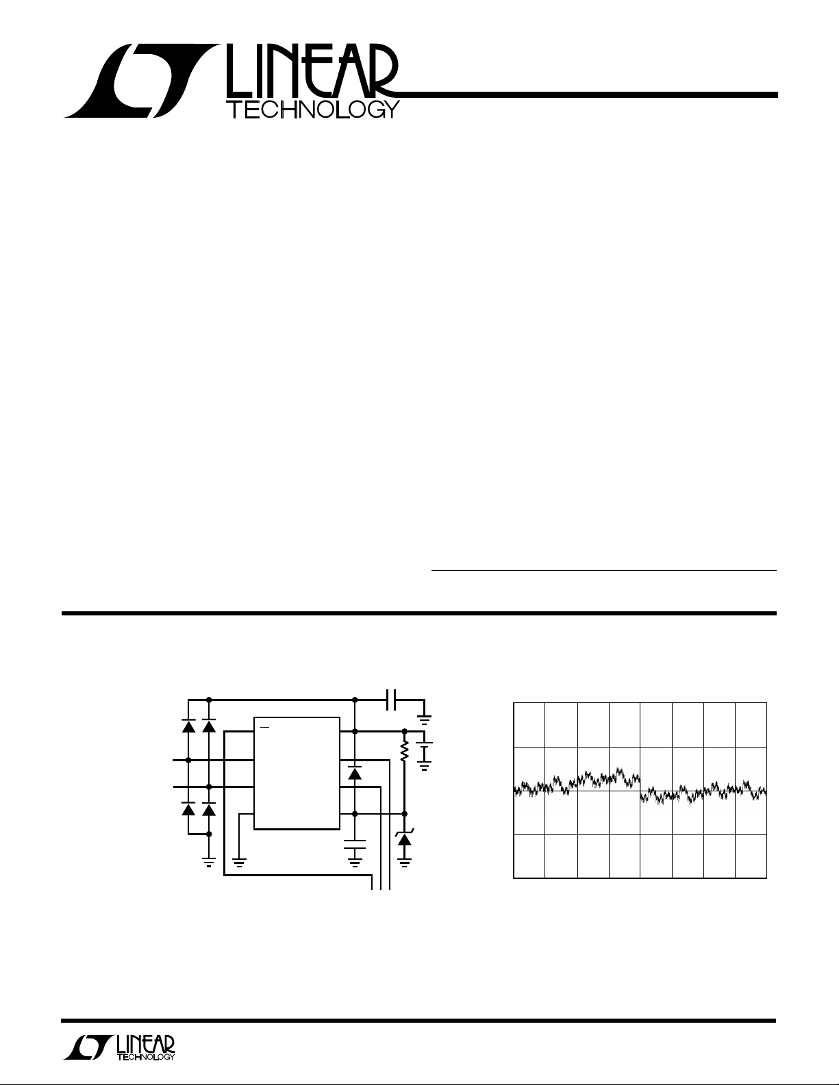
3V Differential Input Data Acquisition System INL with V
LTC1287
TANTALUM
D
V
VCC
CLK
OUT
REF
22µF
CS
DIFFERENTIAL INPUTS
COMMON MODE RANGE
FOR OVERVOLTAGE PROTECTION, LIMIT THE INPUT CURRENT TO 15mA
*
PER PIN OR CLAMP THE INPUTS TO VCC AND GND WITH 1N4148 DIODES.
CONVERSION RESULTS ARE NOT VALID WHEN THE SELECTED CHANNEL OR
OTHER CHANNEL IS OVERVOLTAGED (V
ON OVERVOLTAGE PROTECTION IN THE APPLICATIONS INFORMATION.
0V TO V
+
*
CC
–
+IN
–IN
GND
< GND OR VIN > VCC). SEE SECTION
IN
22µF TANTALUM
+
10k
+
TO AND FROM MPU
3V
LITHIUM
LT1004-1.2
1287 TA01
1.0
0.5
0
ERROR (LSB)
–0.5
–1.0
0
512 1024
1536
REF
2048
CODE
= 1.2V
2560 3072
3584 4096
LTC1287 TA02
1
Page 2
LTC1287
W
O
A
(Notes 1 and 2)
LUTEXI T
S
Supply Voltage (VCC) to GND.................................. 12V
Voltage
Analog and Reference Inputs .... –0.3V to V
Digital Inputs........................................ –0.3V to 12V
Digital Outputs .......................... –0.3V to V
Power Dissipation............................................. 500mW
Operating Temperature Range
LTC1287BI, LTC1287CI ................... –40°C TO 85°C
LTC1287BC, LTC1287CC ....................... 0°C to 70°C
Storage Temperature Range ................ –65°C to 150°C
A
WUW
ARB
U
G
I
+ 0.3V
CC
+ 0.3V
CC
S
PACKAGE
TOP VIEW
1
CS
2
+IN
3
–IN
45
GND
J8 PACKAGE
8-LEAD CERAMIC DIP
N8 PACKAGE
8-LEAD PLASTIC DIP
/
O
RDER I FOR ATIO
ORDER PART
NUMBER
V
8
CC
7
CLK
6
D
OUT
V
REF
LTC1287BIJ
LTC1287CIJ
LTC1287BIN
LTC1287CIN
LTC1287BCJ
LTC1287CCJ
LTC1287BCN
1287 PO
LTC1287CCN
WU
Lead Temperature (Soldering, 10 sec.)................ 300°C
UU W
CO VERTER A D ULTIPLEXER CHARACTERISTICS
LTC1287B
PARAMETER CONDITIONS MIN TYP MAX MIN TYP MAX UNITS
Offset Error VCC = 2.7V (Note 4) ● ±3.0 ±3.0 LSB
Linearity Error (INL) VCC = 2.7V (Notes 4 & 5) ● ±0.5 ±0.5 LSB
Gain Error VCC = 2.7V (Note 4) ● ±0.5 ±1.0 LSB
Minimum Resolution for Which No
Missing Codes are Guaranteed
Analog and REF Input Range (Note 7) V
On Channel Leakage Current (Note 8) On Channel = 3V
Off Channel = 0V
On Channel = 0V
Off Channel = 3V
Off Channel Leakage Current (Note 8) On Channel = 3V ● ±1 ±1 µA
Off Channel = 0V
On Channel = 0V
Off Channel = 3V
● 12 12 Bits
● ±1 ±1 µA
● ±1 ±1 µA
● ±1 ±1 µA
(Note 3)
LTC1287C
(V–) – 0.05V to VCC + 0.05V
U
AC CHARACTERISTICS
SYMBOL PARAMETER CONDITIONS MIN TYP MAX UNITS
f
CLK
t
SMPL
t
CONV
t
CYC
t
dDO
t
dis
t
en
Clock Frequency (Note 6) (Note 9) 0.5 MHz
Analog Input Sample Time See Operating Sequence 1.5 CLK Cycles
Conversion Time See Operating Sequence 12 CLK Cycles
Total Cycle Time See Operating Sequence (Note 6) 14 CLK+ Cycles
Delay Time, CLK↓ to D
Delay Time, CS↑ to D
Delay Time, CLK↓ to D
OUT
OUT
OUT
(Note 3)
LTC1287B/LTC1287C
5.0µs
Data Valid See Test Circuits ● 250 450 ns
Hi-Z See Test Circuits ● 80 160 ns
Enabled See Test Circuits ● 130 250 ns
2
Page 3
LTC1287
AC CHARACTERISTICS
SYMBOL PARAMETER CONDITIONS MIN TYP MAX UNITS
t
hDO
t
f
t
r
t
WHCLK
t
WLCLK
t
suCS
t
WHCS
t
WLCS
C
IN
Time Output Data Remains Valid After CLK↓ 50 ns
D
Fall Time See Test Circuits ● 40 100 ns
OUT
D
Rise Time See Test Circuits ● 40 100 ns
OUT
CLK High Time VCC = 3V (Note 6) 600 ns
CLK Low Time VCC = 3V (Note 6) 800 ns
Setup Time, CS↓ Before CLK↑ VCC = 3V (Note 6) 100 ns
CS High Time Between Data Transfer Cycles VCC = 3V (Note 6) 5.0 µs
CS Low Time During Data Transfer VCC = 3V (Note 6) 14 CLK Cycles
Input Capacitance Analog Inputs On Channel 100 pF
(Note 3)
LTC1287B/LTC1287C
Analog Inputs Off Channel 5 pF
Digital Inputs 5 pF
U
D
DIGITAL
SYMBOL PARAMETER CONDITIONS MIN TYP MAX UNITS
V
IH
V
IL
I
IH
I
IL
V
OH
V
OL
I
OZ
I
SOURCE
I
SINK
I
CC
I
REF
A
High Level Input Voltage VCC = 3.6V ● 2.1 V
Low Level Input Voltage VCC = 3.0V ● 0.45 V
High Level Input Current VIN = V
Low Level Input Current VIN = 0V ● –2.5 µA
High Level Output Voltage VCC = 3.0V, IO = 20µA 2.90 V
Low Level Output Voltage VCC = 3.0V, IO = 20µA 0.05 V
High Z Output Leakage V
Output Source Current V
Output Sink Current V
Positive Supply Current CS High ● 1.5 5 mA
Reference Current V
DC
LECTRICAL C CHARA TER ST
E
CC
IO = 400µA ● 2.7 2.85 V
IO = 400µA ● 0.10 0.3 V
= VCC, CS High ● 3 µA
OUT
V
= 0V, CS High ● –3 µA
OUT
= 0V –10 mA
OUT
= V
OUT
CC
= 2.5V ● 10 50 µA
REF
ICS
I
(Note 3)
LTC1287B/LTC1287C
● 2.5 µA
9mA
The ● denotes specifications which apply over the operating temperature
range; all other limits and typicals TA = 25°C.
Note 1: Absolute Maximum Ratings are those values beyond which the life
of a device may be impaired.
Note 2: All voltage values are with respect to ground (unless otherwise
noted).
Note 3: V
Note 4: One LSB is equal to V
= 2.5V, 1LSB = 2.5V/4096 = 0.61mV.
Note 5: Integral nonlinearity error is defined as the deviation of a code
from a straight line passing through the actual endpoints of the transfer
curve. The deviation is measured from the center of the quantization band.
= 3V, V
CC
= 2.5V, CLK = 500kHz unless otherwise specified.
REF
divided by 4096. For example, when V
REF
REF
Note 6: Recommended operating conditions.
Note 7: Two on-chip diodes are tied to each analog input which will
conduct for analog voltages one diode drop below GND or one diode drop
above V
inputs can cause this input diode to conduct, especially at elevated
temperature, and cause errors for inputs near full scale. This spec allows
50mV forward bias of either diode. This means that as long as the analog
input does not exceed the supply voltage by more than 50mV, the output
code will be correct.
Note 8: Channel leakage current is measured after the channel selection.
Note 9: Increased leakage currents at elevated temperatures cause the S/
H to droop, therefore it is recommended that f
f
CLK
. Be careful during testing at low VCC levels, as high level analog
CC
≥ 30kHz at 85°C and
≥ 3kHz at 25°C.
CLK
3
Page 4
LTC1287
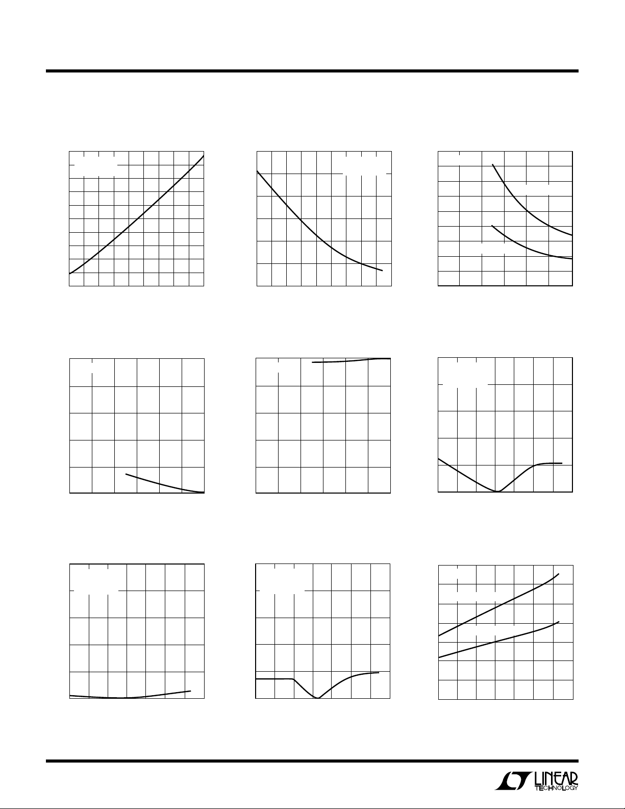
REFERENCE VOLTAGE (V)
0
0
OFFSET (LSB = 1/4096 × V
REF
)
0.1
0.3
0.4
0.5
2.0
0.9
LTC1287 G3
0.2
1.0 3.0
0.6
0.7
0.8
0.5
1.5
2.5
VCC = 3V
VOS = 0.250mV
VOS = 0.125mV
AMBIENT TEMPERATURE (°C)
–40
0
MAGNITUDE OF OFFSET CHANGE (LSB)
0.2
0.5
0
40
60
LTC1287 G6
0.1
0.4
0.3
–20
20
80
100
VCC = 3V
V
REF
= 2.5V
CLK = 500kHz
AMBIENT TEMPERATURE (°C)
–40
200
250
350
20 60
LTC1287 G9
150
100
–20 0
40 80 100
50
0
300
D
OUT
DELAY TIME FROM CLK↓ (ns)
V
CC
= 3V
MSB-FIRST DATA
LSB-FIRST DATA
LPER
F
O
R
ATYPICA
UW
CCHARA TERIST
E
C
ICS
Supply Current vs Supply Voltage
2.8
CLK = 500kHz
2.6
= 25°C
T
A
2.4
2.2
2.0
1.8
1.6
1.4
SUPPLY CURRENT (mA)
1.2
1.0
0.8
2.8 3.0
2.7
2.9
SUPPLY VOLTAGE (V)
3.2 3.6
3.3
3.1
Change in Linearity vs Reference
Voltage
0.5
)
VCC = 3V
REF
0.4
0.3
3.4
3.5
LTC1287 G1
Supply Current vs Temperature
1.9
1.8
1.7
1.6
1.5
SUPPLY CURRENT (mA)
1.4
1.3
–25 5
–40
–10
TEMPERATURE (°C)
35 95
20
Change in Gain vs Reference
Voltage
0
VCC = 3V
)
REF
–0.1
–0.2
CLK = 500kHz
= 3V
V
CC
65
50
LTC1287 G2
Unadjusted Offset Voltage vs
Reference Voltage
80
Change in Offset vs Temperature
0.2
0.1
CHANGE IN LINEARITY (LSB = 1/4096 × V
0
0
1.0 1.5 2.0
0.5
REFERENCE VOLTAGE (V)
Change in Linearity vs
Temperature
0.5
VCC = 3V
= 2.5V
V
REF
CLK = 500kHz
0.4
0.3
0.2
0.1
MAGNITUDE OF LINEARITY CHANGE (LSB)
0
–40
4
0
–20
AMBIENT TEMPERATURE (°C)
–0.3
–0.4
CHANGE IN GAIN (LSB = 1/4096 × V
–0.5
2.5 3.0
LTC1287 G4
0
1.0 1.5 2.0
0.5
REFERENCE VOLTAGE (V)
Change in Gain vs Temperature
0.5
VCC = 3V
= 2.5V
V
REF
CLK = 500kHz
0.4
0.3
0.2
0.1
MAGNITUDE OF GAIN CHANGE (LSB)
0
40
20
60
80
LTC1287 G7
100
–40
0
–20
AMBIENT TEMPERATURE (°C)
40
20
60
2.5 3.0
LTC1287 G5
100
80
LTC1287 G8
D
Delay Time vs Temperature
OUT
Page 5
LPER
REFERENCE VOLTAGE (V)
0
0
PEAK-TO-PEAK NOISE ERROR (LSB)
0.2
0.3
0.4
0.5
0.6
0.7
0.5
1.0
1.5 2.0
LTC1287 G15
2.5
0.8
0.9
1.0
0.1
3.0
LTC1287 NOISE = 200µV
P-P
F
O
R
ATYPICA
UW
CCHARA TERIST
E
C
LTC1287
ICS
Maximum Clock Rate vs Source
Resistance
500
400
300
200
+V
+IN
IN
R
100
MAXIMUM CLK FREQUENCY* (MHz)
0
100
–
SOURCE
–IN
1k 10k 100k
R
SOURCE
VCC = 3V
V
CLK = 500kHz
– (Ω)
REF
= 2.5V
Sample-and-Hold Acquisition
Time vs Source Resistance
100
V
= 2.5V
REF
= 3V
V
CC
= 25°C
T
A
0V TO 2.5V INPUT STEP
R
+
SOURCE
V
IN
10
S & H ACQUISITION TIME TO 0.02% (µs)
1
100 1k 10k
+
–
R
SOURCE
+ (Ω)
LTC G10
LTC1287 G13
Minimum Clock Rate for 0.1LSB
Error**
VCC = 3V
0.25
0.20
0.15
0.10
0.05
MINIMUM CLK FREQUENCY (MHz)
–50
02550
–25
AMBIENT TEMPERATURE (°C)
Input Channel Leakage Current vs
Temperature
1000
900
800
700
600
500
400
300
200
100
INPUT CHANNEL LEAKAGE CURRENT (nA)
0
–30 10
–10
–50
AMBIENT TEMPERATURE (°C)
GUARANTEED
ON CHANNEL
OFF CHANNEL
70 90
50 130
30
75 100
LTC1287 G11
110
LTC1287 G14
Maximum Filter Resistor vs Cycle
Time
10k
R
FILTER
V
IN
C
≥1µF
FILTER
1k
*** (Ω)
100
FILTER
10
MAXIMUM R
1
10 1000 10000
+
–
100
CYCLE TIME (µs)
Noise Error vs Reference Voltage
LTC1287 G12
* MAXIMUM CLK FREQUENCY REPRESENTS THE CLK FREQUENCY AT WHICH A 0.1LSB
SHIFT IN THE ERROR AT ANY CODE TRANSITION FROM ITS 500kHz VALUE IS FIRST
DETECTED.
** AS THE CLK FREQUENCY IS DECREASED FROM 1MHz, MINIMUM CLK FREQUENCY
(∆ERROR ≤ 0.1LSB) REPRESENTS THE FREQUENCY AT WHICH A 0.1LSB SHIFT IN ANY
CODE TRANSITION FROM ITS 500kHz VALUE IS FIRST DETECTED.
U
PI FU CTIO S
# PIN FUNCTION DESCRIPTION
1 CS Chip Select Input A logic low on this input enables the LTC1287.
2, 3 +IN, –IN Analog Inputs These inputs must be free of noise with respect to GND.
4 GND Analog Ground GND should be tied directly to an analog ground plane.
5V
6D
REF
OUT
7 CLK Shift Clock This clock synchronizes the serial data transfer.
8V
CC
*** MAXIMUM R
CHANGE IN FULL SCALE ERROR FROM ITS VALUE AT R
DETECTED.
REPRESENTS THE FILTER RESISTOR VALUE AT WHICH A 0.1LSB
FILTER
= 0Ω IS FIRST
FILTER
UU
Reference Input The reference input defines the span of the A/D converter and must be kept free of noise with respect to GND.
Digital Data Output The A/D conversion result is shifted out of this output.
Positive Supply This supply must be kept free of noise and ripple by bypassing directly to the analog ground plane.
5
Page 6

LTC1287
D
OUT
WAVEFORM 1
(SEE NOTE 1)
2.1V
t
dis
90%
10%
D
OUT
WAVEFORM 2
(SEE NOTE 2)
CS
NOTE 1: WAVEFORM 1 IS FOR AN OUTPUT WITH INTERNAL CONDITIONS SUCH
THAT THE OUTPUT IS HIGH UNLESS DISABLED BY THE OUTPUT CONTROL.
NOTE 2: WAVEFORM 2 IS FOR AN OUTPUT WITH INTERNAL CONDITIONS SUCH
THAT THE OUTPUT IS LOW UNLESS DISABLED BY THE OUTPUT CONTROL.
LTC1287 TC06
BLOCK
W
IDAGRA
8
V
CC
2
+IN
3
–IN
TEST CIRCUITS
On and Off Channel Leakage Current
3V
REGISTER
ANALOG
INPUT MUX
4
GND
I
ON
A
I
OFF
A
INPUT
SHIFT
SAMPLE
AND
HOLD
ON CHANNEL
OFF CHANNEL
COMP
12-BIT
CAPACITIVE
DAC
CLK
D
OUT
OUTPUT
SHIFT
REGISTER
12-BIT
SAR
5
V
REF
CONTROL
AND
TIMING
Voltage Waveforms for D
0.45V
t
dDO
7
CLK
6
D
OUT
1
CS
LTC1287 BD
Delay Time, t
OUT
dDO
2.1V
0.6V
LTC1287 TC03
POLARITY
Load Circuit for t
TEST POINT
D
OUT
3k
100pF
Load Circuit for t
1.5V
D
OUT
6
and t
dis
3V t
t
dis
, tr and t
dDO
3k
100pF
LTC1287 TC1
en
WAVEFORM 2, t
dis
WAVEFORM 1
f
TEST POINT
LTC1287 TC02
LTC1287 TC05
Voltage Waveforms for D
D
OUT
t
en
r
Voltage Waveforms for t
Rise and Fall Times, tr, t
OUT
t
f
dis
f
2.1V
0.6V
LTC1287 TC04
Page 7

TEST CIRCUITS
LTC1287
Voltage Waveforms for t
CS
CLK
D
OUT
PPLICATI
A
U
O
S
I FOR ATIO
WU
U
The LTC1287 is a data acquisition component which
contains the following functional blocks:
1. 12-bit successive approximation capacitive A/D
converter
2. Analog multiplexer (MUX)
3. Sample-and-hold (S/H)
4. Synchronous, half-duplex serial interface
5. Control and timing logic
DIGITAL CONSIDERATIONS
Serial Interface
The LTC1287 communicates with microprocessors and
other external circuitry via a synchronous, half-duplex,
three-wire serial interface (see Operating Sequence). The
clock (CLK) synchronizes the data transfer with each bit
being transmitted on the falling CLK edge. The LTC1287
en
0.6V
t
en
does not require a configuration input word and has no D
B11
LTC1287 TC07
IN
pin. It is permanently configured to have a single differential input and to operate in unipolar mode. A falling CS
initiates data transfer. The first CLK pulse enables D
OUT
After one null bit, the A/D conversion result is output on the
D
line with a MSB-first sequence followed by a LSB-
OUT
first sequence. With the half duplex serial interface the
D
data is from the current conversion. This provides
OUT
easy interface to MSB- or LSB-first serial ports. Bringing
CS high resets the LTC1287 for the next data exchange.
Logic Levels
The logic level standards for this supply range have not
been well defined. What standards that do exist are not
universally accepted. The trip point on the logic inputs of
the LTC1287 is 0.28 × VCC. This makes the logic inputs
compatible with HC-type levels and processors that are
.
t
CYC
CS
CLK
t
SMPL
Hi-Z
D
OUT
B11
B9B10
B7
B8
t
CONV
B4
B5B6
B3
Figure 1. LTC1287 Operating Sequence
B0B1B2
B1
B3
B2
B5B4
B6
B7
B10B9B8
B11
t
SMPL
LTC1287 F01
7
Page 8

LTC1287
U
O
PPLICATI
A
S
I FOR ATIO
specified at 3.3V. The output D
OUT
WU
U
is also compatible with
the above standards. The following summarizes such
levels.
VOH (no load) VCC – 0.1V
VOL (no load) 0.1V
V
OH
V
OL
V
IH
V
IL
The LTC1287 can be driven with 5V logic even when V
0.9 × V
0.1 × V
0.7 × V
0.2 × V
CC
CC
CC
CC
CC
is at 3.3V. This is due to a unique input protection device
that is found on the LTC1287.
Microprocessor Interfaces
The LTC1287 can interface directly (without external hardware) to most popular microprocessor (MPU) synchronous serial formats. If an MPU without a serial interface is
used, then three of the MPU’s parallel port lines can be
programmed to form the serial link to the LTC1287. Many
of the popular MPUs can operate with 3V supplies. For
example the MC68HC11 is an MPU with a serial format
(SPI). Likewise parallel MPUs that have the 8051 type
architecture are also capable of operating at this voltage
range. The code for these processors remains the same
and can be found in the LTC1292 data sheet.
Sharing the Serial Interface
The LTC1287 can share the same two-wire serial interface
with other peripheral components or other LTC1287s
(Figure 2). In this case, the CS signals decide which
LTC1287 is being addressed by the MPU.
ANALOG CONSIDERATIONS
Grounding
The LTC1287 should be used with an analog ground plane
and single point grounding techniques. Do not use wire
wrapping techniques to breadboard and evaluate the device.
To achieve the optimum performance use a PC board. The
ground pin (Pin 4) should be tied directly to the ground
plane with minimum lead length (a low profile socket is
fine). Pin 7 (VCC) should be bypassed to the ground plane
with a 22µ F (minimum value) tantalum with leads as short
as possible and as close as possible to the pin. A 0.1µF
ceramic disk also should be placed in parallel with the
22µF and again with leads as short as possible and as close
to VCC as possible. Figure 3 shows an example of an ideal
LTC1287 ground plane design for a two-sided board. Of
course this much ground plane will not always be possible,
but users should strive to get as close to this ideal as
possible.
Bypassing
For good performance, V
must be free of noise and
CC
ripple. Any changes in the VCC voltage with respect to
ground during a conversion cycle can induce errors or
noise in the output code. VCC noise and ripple can be kept
below 0.5mV by bypassing the VCC pin directly to the
analog plane with a minimum of 22µ F tantalum capacitor
and with leads as short as possible. The lead from the
device to the VCC supply also should be kept to a minimum
and the VCC supply should have a low output impedance
V
0.1µF
CC
2
OUTPUT PORT
SERIAL DATA
8
10
2
22
MPU
Figure 2. Several LTC1287s Sharing One 2-Wire Serial Interface
CS
LTC1287
2 CHANNELS
LTC1287 LTC1287
2 CHANNELS 2 CHANNELS
2
CS
2-WIRE SERIAL
INTERFACE TO OTHER
PERIPHERALS OR LTC1287s
CS
LTC1287 F02
22µF TANTALUM
1
2
LTC1287
3
4
Figure 3. Example Ground Plane for the LTC1287
8
7
6
5
LTC1287 F03/DB
Page 9

LTC1287
PPLICATI
A
U
O
S
I FOR ATIO
WU
U
such as obtained from a voltage regulator (e.g., LT1117).
For high frequency bypassing a 0.1µ F ceramic disk placed
in parallel with the 22µ F is recommended. Again the leads
should be kept to a minimum. Using a battery to power the
LTC1287 will help reduce the amount of bypass capacitance
required on the VCC pin. A battery placed close to the
device will only require 10µF to adequately bypass the
supply pin. Figure 4 shows the effect of poor VCC bypassing.
Figure 5 shows the settling of a LT1117 low dropout
regulator with a 22µF bypass capacitor. The noise and
ripple is kept around 0.5mV. Figure 6 shows the response
of a lithium battery with a 10µF bypass capacitor. The
noise and ripple is kept below 0.5mV.
Analog Inputs
Because of the capacitive redistribution A/D conversion
techniques used, the analog inputs of the LTC1287 have
CC
CS
V
CC
5V/DIV
0.5mV/DIV
HORIZONTAL: 20µs/DIV
Figure 6. Lithium Battery with 10µF Bypassing on V
capacitive switching input current spikes. These current
spikes settle quickly and do not cause a problem. If large
source resistances are used or if slow settling op amps
drive the inputs, take care to insure the transients caused
by the current spikes settle completely before the
conversion begins.
VERTICAL: 0.5mV/DIV
0.5mV/DIV
HORIZONTAL: 10µs/DIV
Figure 4. Poor VCC Bypassing. Noise and
Ripple Can Cause A/D Errors
Source Resistance
The analog inputs of the LTC1287 look like a 100pF
capacitor (CIN) in series with a 1.5k resistor (RON). This
value for RON is for VCC = 2.7V. With larger supply voltages
RON will be reduced. For example, with VCC = 2.7V and V
–
= –2.7V, RON becomes 500Ω. CIN gets switched between
(+) and (–) inputs once during each conversion cycle.
Large external source resistors and capacitances will slow
the settling of the inputs. It is important that the overall RC
time constant is short enough to allow the analog inputs
to settle completely within the allowed time.
“+”
INPUT
+
R
VIN +
CS5V/DIV
VIN –
V
CC
SOURCE
R
SOURCE
C1
“–”
INPUT
–
C2
CS↑
t
WHCS
1/2 CLK
RON = 1.5k
+
LTC1287
CIN =
100pF
LTC1287 F07
HORIZONTAL: 20µs/DIV
Figure 5. LT1117 Regulator with 22µF Bypassing on V
Figure 7. Analog Input Equivalent Circuit
CC
9
Page 10

LTC1287
PPLICATI
A
U
O
S
I FOR ATIO
WU
U
“+” Input Settling
The input capacitor is switched onto the “+” input during
the sample phase (t
sample period can be as short as t
as long as t
+ 1.5 CLK cycles before a conversion
WHCS
, see Figures 8a, 8b and 8c). The
SMPL
+ 0.5 CLK cycle or
WHCS
starts. This variability depends on where CS falls relative
to CLK. The voltage on the “+” input must settle completely
within the sample period. Minimizing R
SOURCE
+ and C1
will improve the settling time. If large “+” input source
“+” and “–” Input Settling Windows
t
WHCS
CS
t
SUCS
D
CLK
OUT
t
(+) INPUT MUST SETTLE DURING THIS TIME
SMPL
HI-Z
resistance must be used, the sample time can be increased
by using a slower CLK frequency. With the minimum
possible sample time of 6.0µ s, R
SOURCE
+ < 4.0k and C1 <
20pF will provide adequate settle time.
“–” Input Settling
At the end of the sample phase the input capacitor switches
to the “–” input and the conversion starts (see Figures 8a,
8b and 8c). During the conversion, the “+” input voltage is
B11
B10
B9
(+) INPUT
(–) INPUT
CLK
D
OUT
(+) INPUT
1ST BIT TEST (–) INPUT MUST
SETTLE DURING THIS TIME
Figure 8a. Setup Time (t
t
WHCS
CS
t
HI-Z
SMPL
1ST BIT TEST (–) INPUT MUST
SETTLE DURING THIS TIME
(+) INPUT MUST SETTLE DURING THIS TIME
SUCS
) is Met
B11
B10
LTC1287 F8a
B9
10
(–) INPUT
Figure 8b. Setup Time (t
SUCS
) is Met
LTC1287 F8b
Page 11

LTC1287
PPLICATI
A
CLK
D
OUT
(+) INPUT
(–) INPUT
U
O
S
I FOR ATIO
CS
WU
t
WHCS
(+) INPUT MUST SETTLE DURING THIS TIME
Figure 8c. Setup Time (t
U
t
SMPL
HI-Z
effectively “held” by the sample and hold and will not affect
the conversion result. It is critical that the “–” input voltage
be free of noise and settle completely during the first CLK
cycle of the conversion. Minimizing R
SOURCE
– and C2 will
improve settling time. If large “–” input source resistance
must be used the time can be extended by using a slower
CLK frequency. At the maximum CLK frequency of 500kHz,
R
SOURCE
– < 200Ω and C2 < 20pF will provide adequate
settling.
Input Op Amps
When driving the analog inputs with an op amp it is
important that the op amp settles within the allowed time
) is Not Met
SUCS
1ST BIT TEST (–) INPUT MUST
SETTLE DURING THIS TIME
B11
B10
LTC1287 F8c
(see Figures 8a, 8b and 8c). Again the “+” and “–” input
sampling times can be extended as described above to
accommodate slower op amps. For single supply low
voltage application the LT1006, LT1013 and LT1014 can
be made to settle well even with the minimum settling
windows of 6µs (“+” input) and 2µs (“–” input) which
occur at the maximum clock rates (CLK = 500kHz).
Figures 9 and 10 show examples of adequate and poor op
amp settling. The LT1077, LT1078 or LT1079 can be used
here to reduce power consumption. Placing an RC network
at the output of the op amps will inprove the settling
response and also reduce the broadband noise.
VERTICAL: 5mV/DIV
HORIZONTAL: 500ns/DIV
Figure 9. Adequate Settling of Op Amp Driving Analog Input
VERTICAL: 5mV/DIV
HORIZONTAL: 20µs/DIV
Figure 10. Poor Op Amp Settling Can Cause A/D Errors
11
Page 12

LTC1287
V2fV
12
f
ERROR(MAX IN PEAK
CLK
)()
=
()
−
π
PPLICATI
A
U
O
S
I FOR ATIO
WU
U
RC Input filtering
It is possible to filter the inputs with an RC network as
shown in Figure 11. For large values of CF (e.g., 1µF) the
capacitive input switching currents are averaged into a net
DC current. A filter should be chosen with a small resistor
and large capacitor to prevent DC drops across the resistor.
The magnitude of the DC current is approximately IDC =
100pF × VIN/t
and is roughly proportional to VIN. When
CYC
running at the minimum cycle time of 33µs, the input
current equals 7.6µ A at VIN = 2.5V. Here a filter resistor of
8Ω will cause 0.1LSB of full-scale error. If a large filter
resistor must be used, errors can be reduced by increasing
the cycle time as shown in the Typical Performance
Characteristics curve Maximum Filter Resistor vs Cycle
Time.
I
FILTER
DC
C
FILTER
“+”
LTC1287
“–”
R
VIN –
Acquisition Time vs Source Resistance). The input voltage
is sampled during the t
time as shown in Figure 8. The
SMPL
sampling interval begins at rising edge of CS and continues
until the falling edge of the CLK before the conversion
begins. On this falling edge the S&H goes into the hold
mode and the conversion begins.
Differential Input
With a differential input the A/D no longer converts a single
voltage but converts the difference between two voltages.
The voltage on the +IN pin is sampled and held and can be
rapidly time varying. The voltage on the –IN pin must
remain constant and be free of noise and ripple throughout
the conversion time. Otherwise the differencing operation
will not be done accurately. The conversion time is 12 CLK
cycles. Therefore a change in the –IN input voltage during
this interval can cause conversion errors. For a sinusoidal
voltage on the –IN input this error would be:
LTC1287 F11
Figure 11. RC Input Filtering
Input Leakage Current
Input leakage currents also can create errors if the source
resistance gets too large. For example, the maximum input
leakage specification of 1µA (at 85°C) flowing through a
source resistance of 1k will cause a voltage drop of 1mV
or 1.6LSB with V
= 2.5V. This error will be much
REF
reduced at lower temperatures because leakage drops
rapidly (see Typical Performance Characteristics curve
Input Channel Leakage Current vs Temperature).
SAMPLE-AND-HOLD
Single-Ended Input
The LTC1287 provides a built-in sample and hold (S&H)
function on the +IN input for signals acquired in the single
ended mode (–IN pin grounded). The sample and hold
allows the LTC1287 to convert rapidly varying signals (see
Typical Performance Characteristics curve of S&H
Where f
V
PEAK
CLK. Usually V
is the frequency of the –IN input voltage,
(–IN)
is its peak amplitude and f
will not be significant. For a 60Hz
ERROR
is the frequency of the
CLK
signal on the –IN input to generate a 0.25LSB error
(150µV) with the converter running at CLK = 500kHz, its
peak value would have to be 16mV. Rearranging the above
equation, the maximum sinusoidal signal that can be
digitized to a given accuracy is given as:
f
IN MAX
()
−
=
ERROR MAX
2V
π
()
PEAK
f
12
CLK
V
For 0.25LSB error (150µV) the maximum input sinusoid
with a 2.5V peak amplitude that can be digitized is 0.4Hz.
Reference Input
The voltage on the reference input of the LTC1287
determines the voltage span of the A/D converter. The
reference input has transient capacitive switching currents due to the switched capacitor conversion technique (see Figure 12). During each bit test of the
12
Page 13

LTC1287
PPLICATI
A
U
O
S
I FOR ATIO
WU
U
conversion (every CLK cycle) a capacitive current spike
will be generated on the reference pin by the A/D. These
current spikes settle quickly and do not cause a problem. If slow settling circuitry is used to drive the
reference input, take care to insure that transients
caused by these current spikes settle completely during
each bit test of the conversion.
REF+
14
R
OUT
V
REF
Figure 12. Reference Input Equivalent Circuit
GND
13
EVERY CLK CYCLE
R
ON
LTC1287
8pF – 40pF
LTC 1287 F12
Figures 13 and 14 show examples of both adequate and
poor settling. Using a slower CLK will allow more time
for the reference to settle. Even at the maximum CLK
rate of 500kHz most references and op amps can be
made to settle within the 2µ s bit time. For example an
LT1019 used in the shunt mode with a 10µF bypass
capacitor will settle adequately. To minimize power an
LT1004-2.5 can be used with a 10µ F bypass capacitor.
For lower value references the LT1004-1.2 with a 10µ F
bypass capacitor can be used.
Reduced Reference Operation
The effective resolution of the LTC1287 can be increased by reducing the input span of the converter.
The LTC1287 exhibits good linearity over a range of
reference voltages (seeTypical Performance Characteristics curves of Change in Linearity vs Reference
Voltage). Care must be taken when operating at low
values of V
because of the reduced LSB step size and
REF
the resulting higher accuracy requirement placed on
the converter. Offset and Noise are factors that must be
considered when operating at low V
REF
values.
VERTICAL: 0.5mV/DIV
HORIZONTAL: 1µs/DIV
Figure 13. Adequate Reference Settling
VERTICAL: 0.5mV/DIV
HORIZONTAL: 10µs/DIV
Figure 14. Poor Reference Settling Can Cause A/D Errors
Offset with Reduced V
REF
The offset of the LTC1287 has a larger effect on the
output code when the A/D is operated with a reduced
reference voltage. The offset (which is typically a fixed
voltage) becomes a larger fraction of an LSB as the size
of the LSB is reduced. The Typical Performance Characteristics curve of Unadjusted Offset Error vs Reference Voltage shows how offset in LSBs is related to
reference voltage for a typical value of VOS. For
example a V
of 0.1mV, which is 0.2LSB with a 2.5V
OS
reference becomes 0.4LSB with a 1.25 reference. If
this offset is unacceptable, it can be corrected digitally
by the receiving system or by offsetting the –IN input to
the LTC1287.
Noise with Reduced V
REF
The total input referred noise of the LTC1287 can be
reduced to approximately 200µ V peak-to-peak using a
ground plane, good bypassing, good layout techniques
and minimizing noise on the reference inputs. This
13
Page 14

LTC1287
PPLICATI
A
U
O
S
I FOR ATIO
WU
U
noise is insignificant with a 2.5V reference input but will
become a larger fraction of an LSB as the size of the LSB
is reduced. The Typical Performance Characteristics
curve of Noise Error vs Reference Voltage shows the
LSB contribution of this 200µV of noise.
For operation with a 2.5V reference, the 200µ V noise is
only 0.32LSB peak-to-peak. Here the LTC1287 noise
will contribute virtually no uncertainty to the output
code. For reduced references, the noise may become a
significant fraction of an LSB and cause undesirable
jitter in the output code. For example, with a 1.25V
reference, this 200µV noise is 0.64LSB peak-to-peak.
This will reduce the range of input voltages over which
a stable output code can be achieved by 0.64LSB. Now
averaging readings may be necessary.
This noise data was taken in a very clean test fixture.
Any setup induced noise (noise or ripple on VCC, V
REF
or VIN) will add to the internal noise. The lower the
reference voltage used, the more critical it becomes to
have a noise-free setup.
Overvoltage Protection
Applying signals to the LTC1287’s analog inputs that
exceed the positive supply or that go below ground will
degrade the accuracy of the A/D and possibly damage
the device. For example this condition would occur if a
signal is applied to the analog inputs before power is
applied to the LTC1287. Another example is the input
source operating from different supplies of larger value
than the LTC1287. These conditions should be prevented either with proper supply sequencing or by use
of external circuitry to clamp or current limit the input
source. There are two ways to protect the inputs. In
Figure 15 diode clamps from the inputs to VCC and GND
are used. The second method is to put resistors in
series with the analog inputs for current limiting. Limit
the current to 15mA per channel. The +IN input can
accept a resistor value of 1k but the –IN input cannot
accept more than 200Ω when clocked at its maximum
clock frequency of 500kHz. If the LTC1287 is clocked at
the maximum clock frequency and 200Ω is not enough
to current limit the input source then the clamp diodes
are recommended (Figures 16 and 17). The reason for
the limit on the resistor value is the MSB bit test is
affected by the value of the resistor placed at the –IN
input (see discussion on Analog Inputs and the Typical
Performance Characteristics curve of Maximum CLK
Frequency vs Source Resistance).
If VCC and V
be turned on first, then V
met, connecting a diode from V
are not tied together, then VCC should
REF
. If this sequence cannot be
REF
to VCC is recom-
REF
mended (see Figure 18).
Because a unique input protection structure is used on
the digital input pins, the signal levels on these pins can
exceed the device V
1N4148 DIODES
Figure 15. Overvoltage Protection for Inputs
1k
200Ω
Figure 16. Overvoltage Protection for Inputs
1N4148 DIODES
1k
Figure 17. Overvoltage Protection for Inputs
without damaging the device.
CC
+3V
LTC1287 F15
+3V
LTC1287 F16
+3V
LTC1287 F17
CS
+IN
–IN
GND
CS
+IN
–IN
GND
CS
+IN
LTC1287
–IN
GND
LTC1287
LTC1287
D
V
V
CLK
OUT
REF
D
V
CC
V
CLK
OUT
REF
V
CC
CLK
D
OUT
V
REF
CC
14
Page 15

LTC1287
PPLICATI
A
U
O
S
I FOR ATIO
CS
+IN
–IN
GND
LTC1287
V
CC
CLK
D
OUT
V
REF
Figure 18
WU
+3V
1N4148
+2.5V
LTC1287 F18
U
A “Quick Look” Circuit for the LTC1287
Users can get a quick look at the function and timing of
the LTC1287 by using the following simple circuit
(Figure 19). V
is tied to VCC. VIN is applied to the +IN
REF
input and the –IN input is tied to the ground plane. CS
is driven at 1/32 the clock rate by the 74HC393 and D
outputs the data. The output data from the D
OUT
OUT
pin can
be viewed on an oscilloscope that is set up to trigger on
the falling edge of CS (Figure 20). Note the LSB data is
partially clocked out before CS goes high.
22µF TANTALUM
+
f/32
CS
V
IN
+IN
–IN
GND
LTC1287
V
CC
CLK
D
OUT
V
REF
f
A1
CLR1
1QA
1QB
1QC
1QD
GND
74HC393
VCC
A2
CLR2
2QA
2QB
2QC
2QD
+3V
0.1µF
TO OSCILLOSCOPE
CLOCK IN
500kHz
Figure 19. "Quick Look" Circuit for the LTC1287
CLK
CS
D
OUT
MSB
NULL
(B11)
BIT
VERTICAL: 5V/DIV
HORIZONTAL: 5µs/DIV
LSB
(B0)
LSB DATA
(B1)
Figure 20. Scope Trace of the LTC1287 “Quick Look” Circuit
Showing A/D Output 1010101010 (AAA
HEX
)
LTC1287 F19
Information furnished by Linear Technology Corporation is believed to be accurate and reliable.
However, no responsibility is assumed for its use. Linear Technology Corporation makes no representation that the interconnection of circuits as described herein will not infringe on existing patent rights.
15
Page 16

LTC1287
PACKAGE DESCRIPTIO
0.290 – 0.320
(7.366 – 8.128)
0.008 – 0.018
(0.203 – 0.460)
0.385 ± 0.025
(9.779 ± 0.635)
0° – 15°
0.038 – 0.068
(0.965 – 1.727)
0.014 – 0.026
(0.360 – 0.660)
U
Dimensions in inches (millimeters) unless otherwise noted.
J8 Package
8-Lead Ceramic DIP
0.405
(10.287)
87
12
0.015 – 0.060
(0.381 – 1.524)
0.100 ± 0.010
(2.540 ± 0.254)
0.200
(5.080)
MAX
0.125
3.175
MIN
0.005
(0.127)
MIN
0.025
(0.635)
RAD TYP
0.055
(1.397)
MAX
MAX
65
3
0.220 – 0.310
(5.588 – 7.874)
4
J8 0392
T
JMAX
150°C 100°C/W
N8 Package
8-Lead Plastic DIP
0.300 – 0.320
(7.620 – 8.128)
0.065
(1.651)
0.009 – 0.015
(0.229 – 0.381)
+0.025
0.325
–0.015
+0.635
8.255
()
–0.381
TYP
0.045 ± 0.015
(1.143 ± 0.381)
(2.540 ± 0.254)
0.045 – 0.065
(1.143 – 1.651)
0.100 ± 0.010
T
JMAX
100°C 130°C/W
θ
JA
0.130 ± 0.005
(3.302 ± 0.127)
0.125
(3.175)
MIN
0.018 ± 0.003
(0.457 ± 0.076)
θ
JA
0.020
(0.508)
MIN
0.400
(10.160)
MAX
876
12
3
5
4
0.250 ± 0.010
(6.350 ± 0.254)
N8 0392
16
Linear Technology Corporation
1630 McCarthy Blvd., Milpitas, CA 95035-7487
(408) 432-1900
●
FAX
: (408) 434-0507
●
TELEX
: 499-3977
LT/GP 0592 10K REV 0
LINEAR TECHNOLOGY CORPORATION 1992
 Loading...