

Page 1
LTC1266
LOAD CURRENT (A)
0.01
80
EFFICIENCY (%)
85
90
95
100
0.1 51
LTC1266 • TA02
VIN = 5V
LTC1266-3.3/LTC1266-5
Synchronous Regulator
Controller for
N- or P-Channel MOSFETs
EATU
F
■
Ultra-High Efficiency: Over 95% Possible
■
Drives N-Channel MOSFET for High Current or
RE
S
P-Channel MOSFET for Low Dropout
■
Pin Selectable Burst Mode Operation
■
1% Output Accuracy (LTC1266A)
■
Pin Selectable Phase of Topside Driver for Boost
or Step-Down Operation
■
Wide VIN Range: 3.5V to 20V
■
On-Chip Low-Battery Detector
■
High Efficiency Maintained over Large Current Range
■
Low 170µA Standby Current at Light Loads
■
Current Mode Operation for Excellent Line and Load
Transient Response
■
Logic Controlled Micropower Shutdown: IQ < 40µA
■
Short Circuit Protection
■
Synchronous Switching with Nonoverlaping Gate Drives
■
Available in 16-Pin Narrow SO Package
U
O
PPLICATI
A
■
Notebook and Palmtop Computers
■
Portable Instruments
■
Cellular Telephones
■
DC Power Distribution Systems
■
GPS Systems
S
DUESCRIPTIO
The LTC®1266 series is a family of synchronous switching
regulator controllers featuring automatic Burst Mode
operation to maintain high efficiencies at low output
currents. These devices drive external power MOSFETs at
switching frequencies up to 400kHz using a constant offtime current mode architecture providing constant ripple
current in the inductor. They can drive either an N-channel
or a P-channel topside MOSFET.
The operating current level is user-programmable via an
external current sense resistor. Wide input supply range
allows operation from 3.5V to 18V (20V maximum).
Constant off-time architecture provides low dropout regulation limited only by the R
of the topside MOSFET
DS(ON)
(when using the P-channel) and the resistance of the
inductor and current sense resistor.
The LTC1266 series combines synchronous switching for
maximum efficiency at high currents with an automatic
low current operating mode, called Burst Mode operation,
which reduces switching losses. Standby power is reduced to only 1mW at VIN = 5V (at I
= 0). Load currents
OUT
in Burst Mode operation are typically 0mA to 500mA.
, LTC and LT are registered trademarks of Linear Technology Corporation.
Burst Mode is a trademark of Linear Technology Corporation.
TM
*COILTRONICS CTXO212801
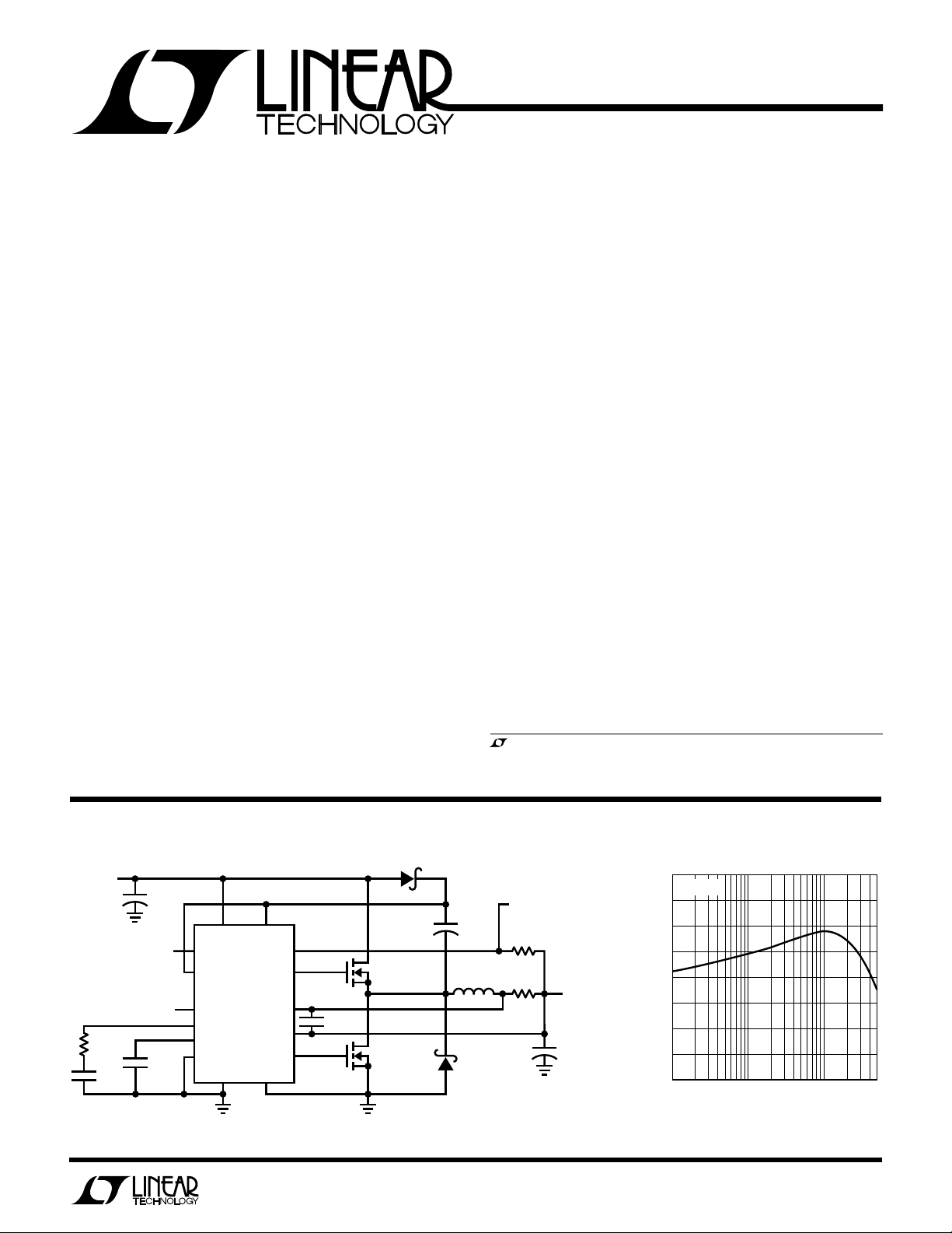
V
IN
4V TO 9V
+
LOW BAT IN
0V = NORMAL
>1.5V = SHUTDOWN
RC
470Ω
CC
3300pF
U
O
A
PPLICATITYPICAL
MBR0530T1
CIN
100µF
×2
CT
180pF
VIN PWR V
LB
IN
PINV
LTC1266-3.3
SHDN
I
TH
C
T
SGND
LB
OUT
TDRIVE
SENSE
SENSE
BDRIVEBINH
PGND
IN
N-CHANNEL
Si9410
+
1000pF
–
N-CHANNEL
Si9410
Figure 1. High Efficiency Step-Down Converter
D2
LOW BAT OUT
CB
0.1µF
L*
5µH
D1
MBRS130LT3
LTC1266 • TA01
100k
R
SENSE
0.02Ω
V
OUT
3.3V
5A
+
C
OUT
330µF
× 2
LTC1266-3.3 Efficiency
1
Page 2
LTC1266
LTC1266 - 3. 3/LTC1266 -5
W
O
A
LUTEXI T
S
Input Supply Voltage (Pins 2, 5)............... 20V to – 0.3V
Continuous Output Current (Pins 1, 16) .............. 50mA
Sense Voltages (Pins 8, 9)........................ 13V to – 0.3V
PINV, BINH, SHDN, LB
(Pins 3, 4, 11, 13) .................................20V to – 0.3V
LB
Output Current ........................................... 12mA
OUT
Operating Ambient Temperature Range ...... 0°C to 70°C
Extended Commercial
Temperature Range ........................... –40°C to 85°C
Junction Temperature (Note 1)............................ 125°C
Storage Temperature Range ................ –65°C to 150°C
Lead Temperature (Soldering, 10 sec)................. 300°C
LECTRICAL C CHARA TERIST
E
SYMBOL PARAMETER CONDITIONS MIN TYP MAX UNITS
V
FB
I
FB
V
OUT
∆V
I
Q1
I
Q2
V
SENSE 1
OUT
Feedback Voltage VIN = 9V, I
LTC1266ACS Topside Switch = N-Ch
LTC1266CS
Feedback Current (LTC1266 Only) ● 0.2 1 µA
Regulated Output Voltage VIN = 9V, I
LTC1266CS-3.3 Topside Switch = N-Ch, V
LTC1266CS-5
Output Ripple (Burst Mode Operation) I
Output Voltage Line Regulation I
Output Voltage Load Regulation 5mA < I
LTC1266-3.3 Burst Mode Operation Enabled, V
LTC1266-3.3 Burst Mode Operation Inhibited, V
LTC1266-5 Burst Mode Operation Enabled, V
LTC1266-5 Burst Mode Operation Inhibited, V
VIN Pin DC Supply Current (Note 2)
Normal Mode 3.5V < V
Sleep Mode 3.5V < V
Shutdown V
PWR VIN DC Supply Current (Note 2)
Normal Mode 3.5V < PWR V
Sleep Mode 3.5V < PWR V
Shutdown V
Current Sense Threshold V
(Burst Mode Operation Enabled)
LTC1266 V
LTC1266-3.3 V
LTC1266-5 V
A
IN
WUW
U
/
TOP VIEW
S PACKAGE
= 125°C, θ
SHDN
O
RDER I FOR ATIO
BDRIVE
16
PGND
15
LB
14
OUT
LB
13
IN
SGND
12
SHDN
11
V
(NC*)
10
FB
+
SENSE
9
= 110°C/W
JA
= V
= 0V unless otherwise noted.
BINH
● 1.275 V
● 1.210 1.25 1.290 V
● 4.90 5.05 5.20 V
LTC1266CS
LTC1266CS-3.3
LTC1266CS-5
LTC1266ACS
ARB
LOAD
LOAD
SHDN
SHDN
BINH
G
S
I
ICS
= 150mA 50 mV
= 50mA
V
PINV
V
PINV
= 2.1V, 3.5V < VIN < 18V 25 50 µA
= 2.1V, 3.5V < PWR VIN < 18V 1 5 µA
= 0V
SENSE
V
SENSE
SENSE
V
SENSE
SENSE
V
SENSE
TA = 25°C, VIN = 10V, V
= 700mA, V
LOAD
= 700mA, V
LOAD
= 0V, Topside Switch = P-Ch, VIN = 7V to 12V –40 0 40 mV
= V
, Topside Switch = N-Ch, VIN = 7V to 12V –40 0 40 mV
PWR
< 2A, R
LOAD
< 18V 2.1 3.0 mA
IN
< 18V 170 250 µA
IN
< 18V 20 40 µA
IN
< 18V 1 5 µA
IN
–
= 3.3V, VFB = V
–
= 3.3V, VFB = V
–
= V
+ 100mV (Forced) 25 mV
OUT
–
= V
– 100mV (Forced) ● 135 155 175 mV
OUT
–
= V
+ 100mV (Forced) 25 mV
OUT
–
= V
– 100mV (Forced) ● 135 155 175 mV
OUT
PACKAGE
TDRIVE
1
PWR V
Consult factory for Industrial and Military grade parts.
= V
PINV
= V
PINV
= 14V ● 3.23 3.33 3.43 V
PWR
= 0.05Ω
SENSE
/2.64 + 25mV (Forced) 25 mV
OUT
/2.64 – 25mV (Forced) ● 135 155 175 mV
OUT
2
IN
PINV
3
BINH
4
V
5
IN
C
6
T
I
7
TH
–
SENSE
8
16-LEAD PLASTIC SO
*FIXED OUTPUT VERSIONS
T
JMAX
,
PWR
,
PWR
= 0V ● 40 65 mV
BINH
= 2V ● 15 25 mV
BINH
= 0V ● 60 100 mV
BINH
= 2V ● 25 40 mV
BINH
WU
ORDER PART
NUMBER
P-P
U
2
Page 3
LTC1266
LTC1266-3.3/LTC1266 -5
LECTRICAL C CHARA TERIST
E
SYMBOL PARAMETER CONDITIONS MIN TYP MAX UNITS
V
SENSE 2
V
SHDN
I
SHDN
I
PINV
V
BINH
I
BINH
I
CT
t
OFF
t
MAX
tr, t
V
CLAMP
V
LBTRIP
I
LBLEAK
I
LBSINK
I
LBIN
Current Sense Threshold V
(Burst Mode Operation Disabled)
LTC1266 V
LTC1266-3.3 V
LTC1266-5 V
Shutdown Pin Threshold 0.6 0.8 2 V
Shutdown Pin Input Current 0V < V
Phase Invert Pin Input Current 0V < V
Burst Mode Operation 0.8 1.2 2 V
Inhibit Pin Threshold
Burst Mode Operation 0V < V
Inhibit Pin Input Current
CT Pin Discharge Current V
Off-Time (Note 3) CT = 390pF, I
Max On-Time V
Driver Output Transition Times CL = 3000pF (Pins 1, 16), VIN = 6V 100 200 ns
f
Output Voltage Clamp in V
Burst Mode Operation Inhibit
LTC1266 Measured at V
LTC1266-3.3 Measured at V
LTC1266-5 Measured at V
Low-Battery Trip Point VIN = 5V 1.14 1.25 1.35 V
Max Leakage Current into Pin 14 V
Max Sink Current into Pin 14 V
Max Leakage Current into Pin 13 V
ICS
= 2.1V
BINH
SENSE
V
SENSE
SENSE
V
SENSE
SENSE
V
SENSE
SENSE
V
= 0V 2 10 µA
OUT
= 0V, VIN = 18V 60 µs
OUT
= 2.1V
BINH
= 12V 1.17 1.30 1.42 V
V
IN
LBOUT
LBOUT
= 18V 0.2 1 µA
LBIN
TA = 25°C, VIN = 10V, V
–
= 3.3V, VFB = V
–
= 3.3V, VFB = V
–
= V
+ 100mV (Forced) –20 mV
OUT
–
= V
– 100mV (Forced) ● 135 155 175 mV
OUT
–
= V
+ 100mV (Forced) –20 mV
OUT
–
= V
– 100mV (Forced) ● 135 155 175 mV
OUT
< 8V, VIN = 16V 1.2 5 µA
SHDN
< 18V, VIN = 18V 0.2 1 µA
PINV
< 18V, VIN = 18V 0.2 1 µA
BINH
+
= V
– 100mV, V
OUT
= 700mA 4 5 6 µs
LOAD
FB
SENSE
SENSE
= 18V, V
= 1V, V
= 2V 25 200 nA
LBIN
= 0V, 2.5V < VIN < 18V 1 8 mA
LBIN
/2.64 + 25mV (Forced) – 20 mV
OUT
/2.64 – 25mV (Forced) ● 135 155 175 mV
OUT
–
= V
SENSE
–
–
OUT
= V
SHDN
= 0V unless otherwise noted.
BINH
– 300mV 50 70 90 µA
1.30 V
3.43
5.20 V
V
–40°C < TA < 85°C (Note 4), VIN = 10V, unless otherwise noted.
SYMBOL PARAMETER CONDITIONS MIN TYP MAX UNITS
V
FB
V
OUT
Feedback Voltage (LTC1266 only) VIN = 9V, I
Regulated Output Voltage VIN = 9V, I
= 700mA 1.21 1.25 1.29 V
LOAD
= 700mA
LOAD
LTC1266-3.3 3.23 3.33 3.43 V
LTC1266-5 4.90 5.05 5.20 V
I
Q1
I
Q2
VIN Pin DC Supply Current (Note 2)
Normal Mode 3.5V < V
Sleep Mode 3.5V < V
Shutdown V
IN
IN
SHUTDOWN
PWR VIN DC Supply Current (Note 2)
Normal Mode 3.5V < PWR V
Sleep Mode 3.5V < PWR V
Shutdown V
SHUTDOWN
< 18V 2.1 3.3 mA
< 18V 170 260 µA
= 2.1V, 3.5V < VIN < 18V 25 60 µA
< 18V 20 50 µA
IN
< 18V 1 7 µA
IN
= 2.1V, 3.5V < PWR VIN < 18V 1 7 µA
3
Page 4
LTC1266
LTC1266 - 3. 3/LTC1266 -5
LECTRICAL C CHARA TERIST
E
SYMBOL PARAMETER CONDITIONS MIN TYP MAX UNITS
V
SENSE1
Sense 2 Current Sense Threshold V
V
SHDN
t
OFF
Current Sense Threshold V
(Burst Mode Operation Enabled)
LTC1266 V
LTC1266-3.3, LTC1266-5 V
(Burst Mode Operation Disabled)
LTC1266 V
LTC1266-3.3, LTC1266-5 V
Shutdown Pin Threshold 0.55 0.8 2 V
Off-Time (Note 3) CT = 390pF, I
BINH
SENSE
V
SENSE
SENSE
V
SENSE
BINH
SENSE
V
SENSE
SENSE
V
SENSE
= 0V
= 2.1V
ICS
–
= 3.3V, VFB = V
–
= 3.3V, VFB = V
–
= V
+ 100mV (Forced) 25 mV
OUT
–
= V
– 100mV (Forced) 135 155 180 mV
OUT
–
3.3V, VFB = V
–
3.3V, VFB = V
–
= V
+ 100mV (Forced) –20 mV
OUT
–
= V
– 100mV (Forced) 130 155 185 mV
OUT
= 700mA 3.8 5 6.5 µs
LOAD
/2.64 + 25mV (Forced) 25 mV
OUT
/2.64 – 25mV (Forced) 135 155 180 mV
OUT
/2.64 + 25mV (Forced) –20 mV
OUT
/2.64 – 25mV (Forced) 130 155 185 mV
OUT
The ● denotes specifications which apply over the full operating
temperature range.
Note 1: T
dissipation P
is calculated from the ambient temperature TA and power
J
according to the following formula:
D
TJ = TA + (PD × 110°C/W)
Note 2: Dynamic supply current is higher due to the gate charge being
delivered at the switching frequency. See Applications Information.
UW
LPER
Efficiency vs Input Voltage
100
FIGURE 1 CIRCUIT
95
90
I
= 5A
LOAD
85
EFFICIENCY (%)
80
75
70
3
567
4
INPUT VOLTAGE (V)
F
I
LOAD
R
O
I
LOAD
= 100mA
ATYPICA
= 2.5A
89
LTC1266 • TPC01
CCHARA TERIST
E
C
Line Regulation Load Regulation
40
FIGURE 1 CIRCUIT
= 1A
I
LOAD
30
20
10
(mV)
0
OUT
∆V
–10
–20
–30
–40
45678
3
Note 3: In applications where R
is placed at ground potential, the off-
SENSE
time increases approximately 40%.
Note 4: The LTC1266, LTC1266-3.3, and LTC1266-5 are not tested and
not quality assurance sampled at –40°C and 85°C. These specifications
are guaranteed by design and/or correlation.
Note 5: Unless otherwise noted the specifications for the LTC1266A are
the same as those for the LTC1266.
ICS
20
FIGURE 1 CIRCUIT
INPUT VOLTAGE (V)
LTC1266 • TPC02
10
0
–10
(mV)
OUT
–20
∆V
–30
–40
–50
9
0
VIN = 9V (Burst Mode
OPERATION ENABLED)
VIN = 5V
VIN = 5V (Burst Mode
OPERATION INHIBITED)
1
2
LOAD CURRENT (A)
3
4
LTC1266 • TPC03
5
4
Page 5
LPER
LOAD CURRENT (A)
0
–40
∆V
OUT
(mV)
–30
–20
–10
30
10
0.5
1.0
20
0
1.5
2.0 2.5
3.0
LTC1266 • TPC06
FIGURE 11 CIRCUIT
V
IN
= 12V (Burst Mode
OPERATION ENABLED)
VIN = 5V
VIN = 5V (Burst Mode
OPERATION INHIBITED)
INPUT VOLTAGE (V)
0
SUPPLY CURRENT (µA)
30
40
50
LTC1266 • TPC09
20
10
0
5
10
15
20
V
IN
PWR V
IN
TEMPERATURE (°C)
0
SENSE VOLTAGE (mV)
100
150
200
80
LTC1266 • TPC12
50
0
–50
20
40
60
100
MAX THRESHOLD
MIN THRESHOLD (Burst Mode
OPERATION INHIBIT)
MIN THRESHOLD (Burst Mode
OPERATION ENABLED)
F
O
R
ATYPICA
UW
CCHARA TERIST
E
C
LTC1266
LTC1266-3.3/LTC1266 -5
ICS
100
95
90
85
EFFICIENCY (%)
80
75
70
3.0
2.5
2.0
1.5
1.0
SUPPLY CURRENT (mA)
0.5
100
80
60
40
OFF-TIME (µs)
20
Efficiency vs Input Voltage
FIGURE 11 CIRCUIT
I
= 1A
LOAD
I
= 100mA
LOAD
4
0
INPUT VOLTAGE (V)
12
8
VIN DC Supply Current
ACTIVE MODE
SLEEP MODE
0
4
0
INPUT VOLTAGE (V)
12
8
Off-Time vs Output Voltage
V
LTC1266-3.3
0
01
OUTPUT VOLTAGE (V)
LTC1266-5
2
34
I
LOAD
SENSE
LTC1266 • TPC10
= 2.5A
16
LTC1266 • TPC04
16
LTC1266 • TPC07
–
= V
OUT
Line Regulation
40
FIGURE 11 CIRCUIT
= 1A
I
LOAD
30
20
10
(mV)
0
OUT
∆V
–10
–20
–30
20
–40
0
812
4
INPUT VOLTAGE (V)
16
LTC1266 • TPC05
Power VIN DC Supply Current
25
20
V
OUT
ACTIVE MODE
SLEEP MODE
4
INPUT VOLTAGE (V)
OUT
= 3.3V
2
4
(VIN – V
8
) Voltage
0°C
25°C
6
) VOLTAGE (V)
OUT
12
16
20
LTC1266 • TPC08
70°C
12108
14
LTC1266 • TPC11
16
15
10
SUPPLY CURRENT (µA)
5
20
0
0
Operating Frequency
vs (VIN – V
3.0
2.5
2.0
1.5
1.0
NORMALIZED FREQUENCY
0.5
5
0
0
Load Regulation
Supply Current in Shutdown
Current Sense Threshold Voltage
5
Page 6

LTC1266
LTC1266 - 3. 3/LTC1266 -5
U
UU
PI FU CTIO S
TDrive (Pin 1): High Current Drive for Topside MOSFET.
This MOSFET can be either P-channel or N-channel, user
selectable by Pin 3. Voltage swing at this pin is from PWR
VIN to ground.
PWR VIN (Pin 2): Power Suppy for Drive Signals. Must be
closely decoupled to power ground (Pin 15).
PINV (Pin 3): Phase Invert. Sets the phase of the topside
driver to drive either a P-channel or an N-channel MOSFET
as follows:
P-channel: Pin 3 = 0V
N-channel: Pin 3 = PWR V
BINH (Pin 4): Burst Mode Operation Inhibit. A CMOS logic
high on this pin will disable the Burst Mode operation
feature forcing continuous operation down to zero load.
VIN (Pin 5): Main Supply Pin.
CT (Pin 6): External Capacitor. CT from Pin 4 to ground sets
the operating frequency. The actual frequency is also
dependent on the input voltage.
ITH (Pin 7): Gain Amplifier Decoupling Point. The current
comparator threshold increases with the Pin 7 voltage.
Sense– (Pin 8): Connects to internal resistive divider
which sets the output voltage in LTC1266-3.3 and
LTC1266-5 versions. Pin 8 is also the (–) input for the
current comparator.
IN
Sense+ (Pin 9): The (+) Input to the Current Comparator.
A built-in offset between Pins 8 and 9 in conjunction with
R
VFB (Pin 10): For the LTC1266 adjustable version, Pin 10
serves as the feedback pin from an external resistive
divider used to set the output voltage. On LTC1266-3.3
and LTC1266-5 versions this pin is not used.
SHDN (Pin 11): When grounded, the LTC1266 series
operates normally. Pulling Pin 11 high holds both MOSFETs
off and puts the LTC1266 in micropower shutdown mode.
Requires CMOS logic signal with tr, tf < 1µ s. Should not be
left floating.
SGND (Pin 12): Small-Signal Ground. Must be routed
separately from other grounds to the (–) terminal of C
LBIN (Pin 13): Input to the Low-Battery Comparator. This
input is compared to an internal 1.25V reference.
LB
Comparator. This pin will sink current when Pin 13 is
below 1.25V.
PGND (Pin 15): Driver Power Ground. Connects to source
of N-channel MOSFET and the (–) terminal of CIN.
BDrive (Pin 16): High Current Drive for Bottom N-Channel MOSFET. Voltage swing at Pin 16 is from ground to
PWR VIN.
sets the current trip threshold.
SENSE
(Pin 14): Open Drain Output of the Low-Battery
OUT
OUT
.
6
Page 7

UUW
FU CTIO AL DIAGRA
V
IN
LTC1266
LTC1266-3.3/LTC1266 -5
Pin 10 Connection Shown for LTC1266-3.3 and LTC1266-5; Changes Create LTC1266
LB
LB
13
IN
1.25V
REFERENCE
–
LB
+
14
OUT
SLEEP
SIGNAL
GROUND
12
S
PWR V
2
IN
16 4
15
BDRIVE
PGND
PINV
3
TDRIVE
1
BINH
SENSE
9
+
ADJUSTABLE
VERSION
V
FB
10
SENSE
8
–
–
V
+
–
C
PINV
+
I
TH
V
TRIP
+
–
V
–
13k
7
G
+
REFERENCE
11 5
SHDN V
OS
1.25V
IN
5pF
100k
LTC1266 • FD
–
+
R
Q
S
T
OFF-TIME
CONTROL
V
IN
SENSE
V
FB
–
MAX
ON-TIME
CONTROL
ENABLE
+
–
V
TH2
V
TH1
6
C
T
U
OPERATIO
The LTC1266 series uses a current mode, constant offtime architecture to synchronously switch an external pair
of power MOSFETs. Operating frequency is set by an
external capacitor at the timing capacitor Pin 6.
The output voltage is sensed by an internal voltage divider
connected to Sense–, Pin 8, (LTC1266-3.3 and LTC1266-
5) or external divider returned to VFB, Pin 10, (LTC1266).
A voltage comparator V, and a gain block G, compare the
divided output voltage with a reference voltage of 1.25V.
To optimize efficiency, the LTC1266 automatically switches
between two modes of operation, burst and continuous.
The voltage comparator is the primary control element
when the device is in Burst Mode operation, while the gain
block controls the output voltage in continuous mode.
During the switch ON cycle in continuous mode, current
comparator C monitors the voltage between Pins 8 and 9
connected across an external shunt in series with the
inductor. When the voltage across the shunt reaches its
threshold value, the topside driver output is switched to
turn off the topside MOFSET (Power VIN for P-channel or
ground for N-channel). The timing capacitor connected to
Pin 6 is now allowed to discharge at a rate determined by
the off-time controller. The discharge current is made
proportional to the output voltage (measured by Pin 8) to
model the inductor current, which decays at a rate which
is also proportional to the output voltage. While the timing
capacitor is discharging, the bottom-side drive output is
switched to power VIN to turn on the bottom-side
N-channel MOSFET.
7
Page 8

LTC1266
LTC1266 - 3. 3/LTC1266 -5
U
OPERATIO
When the voltage on the timing capacitor has discharged
past V
causes the bottom-side output to switch off and the
topside output to switch on (ground for P-channel and
Power VIN for N-channel). The cycle then repeats.
As the load current increases, the output voltage decreases
slightly. This causes the output of the gain stage (Pin 7) to
increase the current comparator threshold, thus tracking
the load current.
The sequence of events for Burst Mode operation is very
similar to continuous operation with the cycle interrupted
by the voltage comparator. When the output voltage is at
or above the desired regulated value, the topside MOSFET
is held off by comparator V and the timing capacitor
continues to discharge below V
capacitor discharges past V
trips, causing the internal sleep line to go low and the
bottom-side MOSFET to turn off.
The circuit now enters sleep mode with both power
MOSFETs turned off. In sleep mode, a majority of the
circuitry is turned off, dropping the quiescent current
from 2.1mA to 170µA. The load current is now being
supplied from the output capacitor. When the output
voltage has dropped by the amount of hysteresis in
comparator V, the topside MOSFET is again turned on
and this process repeats.
To avoid the operation of the current loop interfering with
Burst Mode operation, a built-in offset VOS is incorporated
in the gain stage. This prevents the current comparator
threshold from increasing until the output voltage has
dropped below a minimum threshold.
, comparator T trips, setting the flip-
TH1
. When the timing
TH1
, voltage comparator S
TH2
flop. This
To prevent both the external MOSFETs from ever being
turned on at the same time, feedback is incorporated to
sense the state of the driver output pins. Before the
bottom-side drive output can turn on, the topside output
must be off. Likewise, the topside output is prevented
from turning on while the bottom-side drive output is
still on.
The LTC1266 has two select pins which provide the user
with choice of topside switch and with the option of
inhibiting Burst Mode operation. The phase select pin
allows the user to choose whether the topside MOSFET
is a P-channel or an N-channel. The phase select pin does
two things: sets the proper phase of the drive signal (ON
= Power VIN for N-channel and ON = 0V for P-channel)
and also sets an upper limit for the on-time (60µ s) when
set to the N-channel. The on-time limit ensures proper
start-up when used in a single supply bootstrap circuit
configuration (see Applications Information). In P-channel
mode there is no on-time limit and thus, in dropout, the
P-channel MOSFET is turned on continuously (100%
duty cycle).
The Burst Mode operation inhibit (BINH, Pin 4) allows the
Burst Mode operation to be disabled by applying a CMOS
logic high to this pin. With Burst Mode operation disabled,
the LTC1266 will remain in continuous mode down to zero
load. Burst Mode operation is disabled by allowing the
lower current threshold limit to go below zero so that the
voltage comparator will never trip. The voltage comparator
trip point is also raised up so that it will not be tripped by
transients. It is still active to provide a voltage clamp to
prevent the output from overshooting.
WUU U
APPLICATIO S I FOR ATIO
One of the three basic LTC1266 application circuits is
shown in Figure 1. This circuit uses an N-channel
topside driver and a single supply. The other two circuit
configurations (see Typical Applications) use an
N-channel topside driver and dual supply, and a
P-channel topside driver. Selections of other external
components are driven by the load requirement and are
the same for all three circuit configurations. The first
8
step is the selection of R
CT and L can be chosen. Next, the power MOSFETs and
D1 are selected. Finally, CIN and C
the loop is compensated. Using an N-channel topside
switch, input voltages are limited to a maximum of
about 15V. With a P-channel, the input voltage may be
as high as 20V.
SENSE
. Once R
OUT
is known,
SENSE
are selected and
Page 9

WUU U
FREQUENCY (kHz)
0
0
CAPACITANCE (pF)
200
400
100 200 300
400
LTC1266 • F03
600
800
500
VIN = 12V
VIN = 5V
V
OUT
= 3.3V
APPLICATIO S I FOR ATIO
LTC1266
LTC1266-3.3/LTC1266 -5
R
R
Selection for Output Current
SENSE
is chosen based on the required output current.
SENSE
The LTC1266 series current comparator has a threshold
range which extends from a minimum of 25mV/R
SENSE
(when Burst Mode operation is enabled) to a maximum of
155mV/R
. The current comparator threshold sets
SENSE
the peak of the inductor ripple current, yielding a maximum output current I
equal to the peak value less half
MAX
the peak-to-peak ripple current. For proper Burst Mode
operation, I
RIPPLE(P-P)
must be less than or equal to the
minimum current comparator threshold.
Since efficiency generally increases with ripple current,
the maximum allowable ripple current is assumed, i.e.,
I
RIPPLE(P-P)
Operating Frequency). Solving for R
= 25mV/R
(see CT and L Selection for
SENSE
and allowing
SENSE
a margin for variations in the LTC1266 series and
external component values yields:
R
SENSE
A graph for selecting R
=
100mV
I
MAX
vs maximum output
SENSE
current is given in Figure 2.
100
I
BURST
I
SC(PK)
The LTC1266 series automatically extends t
≈
=
15mV
R
SENSE
155mV
R
SENSE
during a
OFF
short circuit to allow sufficient time for the inductor
current to decay between switch cycles. The resulting
ripple current causes the average short circuit current
I
SC(AVG)
to be reduced to approximately I
MAX
.
L and CT Selection for Operating Frequency
The LTC1266 series uses a constant off-time architecture
with t
determined by an external timing capacitor CT.
OFF
Each time the topside MOSFET switch turns on, the
voltage on CT is reset to approximately 3.3V. During the
off-time, CT is discharged by a current which is proportional to V
. The voltage on CT is analogous to the
OUT
current in inductor L, which likewise decays at a rate
proportional to V
. Thus the inductor value must track
OUT
the timing capacitor value.
The value of CT is calculated from the desired continuous
mode operating frequency, f:
The load current, below which Burst Mode operation
commences, (I
rent, (I
chosen, I
following:
75
(mΩ)
50
SENSE
R
25
0
0
), both track I
SC(PK)
BURST
2
4
6
MAXIMUM OUTPUT CURRENT (A)
Figure 2. Selecting R
), and the peak short circuit cur-
BURST
MAX
and I
SC(PK)
SENSE
. Once R
can be predicted from the
8
LTC1266 • F02
10
SENSE
has been
CT =
assumes VIN = 2V
1
2.6 × 10
4
× f
, (Figure 1 circuit).
OUT
A graph for selecting CT vs frequency including the effects
of input voltage is given in Figure 3.
Figure 3. Timing Capacitor Value
9
Page 10

LTC1266
LTC1266 - 3. 3/LTC1266 -5
WUU U
APPLICATIO S I FOR ATIO
As the operating frequency is increased the gate charge
losses will be higher, reducing efficiency (see Efficiency
Considerations). The complete expression for operating
frequency of the circuit in Figure 1 is given by:
1 –
)
V
OUT
V
IN
)
V
REG
)
)
V
OUT
REG/VOUT
× CT × V
SENSE
A consequence of this is that
= 1 in regulation.
REG
OUT
is the
SENSE
1
f =
t
OFF
where:
t
= 1.3 × 10⁴ × CT ×
OFF
V
is the desired output voltage (i.e., 5V, 3.3V). V
REG
measured output voltage. Thus V
Once the frequency has been set by CT, the inductor L
must be chosen to provide no more than 25mV/R
of peak-to-peak inductor ripple current. This results in
a minimum required inductor value of:
L
= 5.1 × 10⁵ × R
MIN
As the inductor value is increased from the minimum
value, the ESR requirements for the output capacitor
are eased at the expense of efficiency. If too small an
inductor is used, the inductor current will decrease past
zero and change polarity.
the LTC1266 series may not enter Burst Mode operation
and efficiency will be slightly degraded at low currents.
Inductor Core Selection
Once the minimum value for L is known, the type of
inductor must be selected. The highest efficiency will be
obtained using ferrite, Kool Mµ® on molypermalloy (MPP)
cores. Lower cost powdered iron cores provide suitable
performance but cut efficiency by 3% to 7%. Actual core
loss is independent of core size for a fixed inductor value,
but it is very dependent on inductance selected. As inductance increases, core losses go down. Unfortunately,
increased inductance requires more turns of wire and
therefore copper losses increase.
rent is exceeded. This results in an abrupt increase in
inductor ripple current and consequent output voltage
ripple which can cause Burst Mode operation to be falsely
triggered. Do not allow the core to saturate!
Kool Mµ is a very good, low loss core material for toroids,
with a “soft” saturation characteristic. Molypermalloy is
slightly more efficient at high (>200kHz) switching frequency. Toroids are very space efficient, especially when
you can use several layers of wire. Because they generally
lack a bobbin, mounting is more difficult. However, new
designs for surface mount are available from Coiltronics
and Beckman Industrial Corp. which do not increase the
height significantly.
Power MOSFET and D1 Selection
Two external power MOSFETs must be selected for use
with the LTC1266 series: either a P-channel MOSFET or an
N-channel MOSFET for the main switch and an N-channel
MOSFET for the synchronous switch. The main selection
criteria for the power MOSFETs are the type of MOSFET,
threshold voltage V
The cost and maximum output current determine the type
of MOSFET for the topside switch. N-channel MOSFETs
have the advantage of lower cost and lower R
expense of slightly increased circuit complexity. For lower
current applications where the losses due to R
small, a P-channel MOSFET is recommended due to the
lower circuit complexity. However, at load currents in
excess of 3A where the R
portion of the total power loss, an N-channel is strongly
recommended to maximize efficiency.
The maximum output current I
requirement for the two MOSFETs. When the LTC1266
series is operating in continuous mode, the simplifying
assumption can be made that one of the two MOSFETs is
always conducting the average load current. The duty
cycles for the two MOSFETs are given by:
and on-resistance R
GS(TH)
becomes a significant
DS(ON)
determines the R
MAX
DS(ON)
DS(ON)
DS(ON)
.
at the
are
DS(ON)
Ferrite designs have very low core loss, so design goals
can concentrate on copper loss and preventing saturation.
Ferrite core material saturates “hard,” which means that
inductance collapses abruptly when the peak design cur-
Kool Mµ is a registered trademark of Magnetics, Inc.
10
V
TopSide Duty Cycle =
Bottom-Side Duty Cycle =
OUT
V
IN
– V
V
IN
V
IN
OUT
Page 11

WUU U
APPLICATIO S I FOR ATIO
LTC1266
LTC1266-3.3/LTC1266 -5
From the duty cycles, the required R
DS(ON)
for each
MOSFET can be derived:
× PT
V
TS R
BS R
DS(ON)
DS(ON)
=
=
V
(V
OUT
IN
× I
– V
IN
MAX
OUT
2
× (1 + δT)
× PB
V
IN
) × I
MAX
2
× (1 + δB)
where PT and PB are the allowable power dissipations and
δT and δB are the temperature dependencies of R
DS(ON)
. P
T
and PB will be determined by efficiency and/or thermal
requirements (see Efficiency Considerations). For a MOSFET,
(1 + δ) is generally given in the form of a normalized
R
δ
vs temperature curve, but δ
DS(ON)
= 0.005/°C can be used as an approximation for low
NCH
= 0.007/°C and
PCH
voltage MOSFETs.
The minimum input voltage determines whether standard
threshold or logic-level threshold MOSFETs must be used.
For VIN > 8V, standard threshold MOSFETs (V
GS(TH)
< 4V)
may be used. If VIN is expected to drop below 8V, logiclevel threshold MOSFETs (V
< 2.5V) are strongly
GS(TH)
recommended. The LTC1266 series Power VIN must always be less than the absolute maximum VGS ratings for
the MOSFETs.
The Schottky diode D1 shown in Figure 1 only conducts
during the deadtime between the conduction of the two
power MOSFETs. D1’s sole purpose in life is to prevent the
body diode of the bottom-side MOSFET from turning on
and storing charge during the deadtime, which could cost
as much as 1% in efficiency (although there are no other
harmful effects if D1 is omitted). Therefore, D1 should be
selected for a forward voltage of less than 0.7V when
conducting I
CIN and C
MAX
Selection
OUT
.
In continuous mode, the current through the topside
MOSFET is a square wave of duty cycle V
OUT/VIN
. To
prevent large voltage transients, a low ESR (Effective
Series Resistance) input capacitor sized for the maximum
RMS current must be used. The maximum RMS capacitor
current is given by:
1/2
)]
CIN Required I
RMS
≈ I
MAX
[V
OUT(VIN – VOUT
V
IN
This formula has a maximum at VIN = 2V
I
= I
RMS
/2. This simple worst-case condition is com-
OUT
OUT
, where
monly used for design because even significant deviations do not offer much relief. Note that capacitor
manufacturer’s ripple current ratings are often based on
only 2000 hours of life. This makes it advisable to further
derate the capacitor, or to choose a capacitor rated at a
higher temperature than required. Always consult the
manufacturer if there is any question. An additional 0.1µF
to 1µF ceramic capacitor is also required on Power V
IN
(Pin 2) for high frequency decoupling.
The selection of C
ESR of C
must be less than twice the value of R
OUT
is driven by the required ESR.
OUT
The
SENSE
for proper operation of the LTC1266 series:
C
Required ESR < 2R
OUT
SENSE
Optimum efficiency is obtained by making the ESR equal
to R
. As the ESR is increased up to 2R
SENSE
SENSE
, the
efficiency degrades by less than 1%. If the ESR is greater
than 2R
, the voltage ripple on the output capacitor
SENSE
will prematurely trigger Burst Mode operation, resulting in
disruption of continuous mode and an efficiency hit which
can be several percent. If Burst Mode operation is disabled, the ESR requirement can be relaxed and is limited
only by the allowable output voltage ripple.
Manufacturers such as Nichicon and United Chemicon
should be considered for high performance capacitors.
The OS-CON semiconductor dielectric capacitor available
from Sanyo has the lowest ESR/size ratio of any aluminum
electrolytic at a somewhat higher price. Once the ESR
requirement for C
rating generally far exceeds the I
has been met, the RMS current
OUT
RIPPLE(P-P)
requirement.
In surface mount applications multiple capacitors may
have to be paralleled to meet the capacitance, ESR or RMS
current handling requirements of the application. An
excellent choice is the AVX TPS series of surface mount
tantalums.
At low supply voltages, a minimum capacitance at C
OUT
is needed to prevent an abnormal low frequency operating mode (see Figure 4). When C
is made too
OUT
small, the output ripple at low frequencies will be large
enough to trip the voltage comparator. This causes
Burst Mode operation to be activated when the LTC1266
11
Page 12

LTC1266
LTC1266 - 3. 3/LTC1266 -5
WUU U
APPLICATIO S I FOR ATIO
1000
800
600
(µF)
OUT
C
400
200
0
0
Figure 4. Minimum Value of C
series would normally be in continuous operation. The
output remains in regulation at all times. This minimum
capacitance requirement may be relaxed if Burst Mode
operation is disabled.
N-Channel vs P-Channel MOSFETs
The LTC1266 has the capability to drive either an
N-channel or a P-channel topside switch to give the user
more flexibility. N-channel MOSFETs are superior in performance to P-channel due to their lower R
lower gate capacitance and are typically less expensive;
however, they do have a slightly more complicated gate
drive requirement and a more limited input voltage range
(see following sections).
1
(VIN – V
L = 50µH
R
SENSE
L = 25µH
R
SENSE
R
SENSE
2
) VOLTAGE (V)
OUT
= 0.02Ω
= 0.02Ω
L = 50µH
= 0.05Ω
3
4
LTC1266 • F04
OUT
5
DS(ON)
and
Driving N-Channel Topside MOSFETs
Driving an N-channel topside MOSFET (PINV, Pin 3, tied to
PWR VIN) is a little trickier than driving a P-channel since
the gate voltage must be positive with respect to the
source to turn it on, which means that the gate voltage
must be higher than VIN. This requires either a second
supply at least V
above VIN or a bootstrapping circuit
GS(ON)
to boost the VIN to the proper level. The easiest method is
using a higher supply (see Figure 14) but if one is not
available, the bootstrap method can be used at the expense of an additional diode (see Figure 1). The bootstrap
works by charging the bootstrap capacitor to VIN during
the off-time. During the on-time, the bottom plate of the
capacitor is pulled up to VIN so that the voltage at Pin 2 is
now twice V
(plus any ringing on the switch node).
IN
Since the maximum allowable voltage at Pin 2 is 20V, the
Figure 1 bootstrap circuit limits VIN to less than 10V. A
higher VIN can be achieved if the bootstrap capacitor is
charged to a voltage less than VIN, in which case
V
IN(MAX)
= 20 – V
CAP
.
N-channel mode, internal circuitry limits the maximum
on-time to 60µs to guarantee start-up of the bootstrap
circuit. This maximum on-time reduces the maximum
duty cycle to:
Max Duty Cycle =
60µs
60µs + t
OFF
Driving P-Channel Topside MOSFETs
The P-channel topside switch circuit configuration is the
most straightforward due to the requirement of only one
supply voltage level. This is due to the negative gate
threshold of the P-channel MOSFET which allows the
MOSFET to be switched on and off by swinging the gate
between VIN and ground. The phase invert (Pin 3) is tied
to ground to choose this operating mode. Normally, the
converter input (VIN) is connected to the LTC1266 supply
Pins 2 and 5 and can go as high as 20V. Pin 2 supplies the
high frequency current pulses to switch the MOSFETs and
should be decoupled with a 0.1µF to 1µ F ceramic capaci-
tor. Pin 5 supplies most of the quiescent power to the rest
of the chip.
12
which slightly increases the minimum input voltage at
which dropout occurs. However, because of the superior
on-conductance of the N-channel, the dropout performance of an all N-channel regulator is still better (see
Figure 5) even with the duty cycle limitation, except at light
loads.
Low-Battery Comparator
The LTC1266 has an on-chip low-battery comparator
which can be used to sense a low-battery condition when
implemented as shown in Figure 6. The resistor divider
R1, R2 sets the comparator trip point as follows:
V
TRIP
= 1.25
1 +
)
R2
R1
)
Page 13

WUU U
LOAD CURRENT (A)
0.01
60
EFFICIENCY (%)
70
80
90
100
0.1 51
LTC1266 • F07
Burst Mode OPERATION
ENABLED
Burst Mode OPERATION
INHIBITED
APPLICATIO S I FOR ATIO
600
V
= 3.3V
OUT
500
TOPSIDE
P-CHANNEL
400
300
(mV) AT DROPOUT
0UT
200
–V
IN
V
100
TOPSIDE N-CHANNEL
WITH POWER V
TOPSIDE
N-CHANNEL WITH
CHARGE PUMP
= 12V
IN
LTC1266
LTC1266-3.3/LTC1266 -5
The divided down voltage at the “–” input to the comparator
is compared to an internal 1.25V reference. This reference
is separate from the 1.25V reference used by the voltage
comparator and current comparator for regulation and is
not disabled by the shutdown pin, therefore the low-battery
detection is operational even when the rest of the chip is
shut down. The comparator is functional down to an input
voltage of 2.5V. Thus, the output will provide a valid state
even when the rest of the chip does not have sufficient
voltage to operate. For best performance, the value of the
pull-up resistor should be high enough that the output is
pulled down to ground when sinking 200µA or less.
Suppressing Burst Mode Operation
Normally, enabling Burst Mode operation is desired due to
its superior efficiency at low load currents (see Figure 7).
However, in certain applications it may be desirable to
inhibit this feature. Some reasons for doing so are:
1. To eliminate audible noise from certain types of induc-
0
1
0
LOAD CURRENT
3
2
4
Figure 5. Comparison of Dropout Performance
V
IN
R2
–
R1
+
1.25V
REFERENCE
LTC1266
LTC1266 • F06
Figure 6. Low-Battery Comparator
tors at light loads.
LTC1266 • F05
5
Figure 7. Effect of Disabling Burst Mode Operation on Efficiency
2. If the load is never expected to drop low enough to
benefit from the efficiency advantages of Burst Mode
LB
OUT
operation, the output capacitor ESR and minimum
capacitance requirements (which may falsely trigger
Burst Mode operation if not met) can be relaxed if Burst
Mode operation is disabled.
3. If an auxiliary winding is used. Disabling Burst Mode
operation guarantees switching independent of the
load on the primary. This allows power to be taken from
the auxiliary winding independently.
4. Tighter load regulation (< 1%).
Burst Mode operation is disabled by applying a CMOS
logic high voltage (> 2.1V) to Pin 4. When it is disabled, the
voltage comparator limit is raised high enough so that it no
longer is involved in regulation; however it is still active
and is useful as a voltage clamp to keep the output from
overshooting.
Note that since the inductor current must reverse to
regulate the output at zero load when Burst Mode operation is disabled, the minimum inductance (L
) specified
MIN
during Inductor Core Selection is no longer applicable.
Checking Transient Response
The regulator loop response can be checked by looking at
the load transient response. Switching regulators take
several cycles to respond to a step in DC (resistive) load
current. When a load step occurs, V
amount equal to ∆I
series resistance of C
(ESR), where ESR is the effective
LOAD
OUT
. ∆I
also begins to charge or
LOAD
shifts by an
OUT
13
Page 14

LTC1266
LTC1266 - 3. 3/LTC1266 -5
WUU U
APPLICATIO S I FOR ATIO
discharge C
current change and returns V
During this recovery time V
until the regulator loop adapts to the
OUT
to its steady-state value.
OUT
can be monitored for
OUT
overshoot or ringing which would indicate a stability
problem. The Pin 7 external components shown in the
Figure 1 circuit will prove adequate compensation for
most applications.
Efficiency Considerations
The percent efficiency of a switching regulator is equal to
the output power divided by the input power times 100%.
It is often useful to analyze individual losses to determine
what is limiting the efficiency and which change would
produce the most improvement. Percent efficiency can be
expressed as:
% Efficiency = 100% – (L1 + L2 + L3 + ...)
where L1, L2, etc., are the individual losses as a percentage of input power. (For high efficiency circuits, only small
errors are incurred by expressing losses as a percentage
of output power).
Although all dissipative elements in the circuit produce
losses, three main sources usually account for most of the
losses in LTC1266 series circuits: 1) LTC1266 DC bias
current, 2) MOSFET gate charge current and 3) I2R losses.
1. The DC supply current is the current which flows into
VIN (Pin 2). For VIN = 10V the LTC1266 DC supply
current is 170µ A for no load, and increases proportionally with load up to a constant 2.1mA after the LTC1266
series has entered continuous mode. Because the DC
bias current is drawn from VIN, the resulting loss
increases with input voltage. For VIN = 5V the DC bias
losses are generally less than 1% for load currents over
30mA. However, at very low load currents the DC bias
current accounts for nearly all of the loss.
2. MOSFET gate charge current results from switching the
gate capacitance of the power MOSFETs. Each time a
MOSFET gate is switched from low to high to low again,
a packet of charge dQ moves from Power VIN to ground.
The resulting dQ/dt is a current flowing into Power V
IN
(Pin 5) which is typically much larger than the DC
supply current. In continuous mode, I
GATECHG
= f (QN +
QP). The typical gate charge for a 0.05Ω N-channel
power MOSFET is 15nC. This results in I
GATECHG
= 6mA
in 200kHz continuous operation for a 2% to 3% typical
mid-current loss with VIN = 5V.
Note that the gate charge loss increases directly with
both input voltage and operating frequency. This is the
principal reason why the highest efficiency circuits
operate at moderate frequencies. Furthermore, it argues against using larger MOSFETs than necessary to
control I2R losses, since overkill can cost efficiency as
well as money!
3. I2R losses are easily predicted from the DC resistances
of the MOSFET, inductor and current shunt. In continuous mode the average output current flows through L
and R
, but is “chopped” between the topside and
SENSE
bottom-side MOSFETs. If the two MOSFETs have approximately the same R
, then the resistance of
DS(ON)
one MOSFET can simply be summed with the resistances of L and R
example, if each R
R
= 0.02Ω, then the total resistance is 0.12Ω. This
SENSE
to obtain I2R losses. For
SENSE
= 0.05Ω, RL = 0.05Ω and
DS(ON)
results in losses ranging from 3.5% to 15% as the
output current increases from 1A to 5A. I2R losses
cause the efficiency to roll off at high output currents.
Figure 8 shows how the efficiency losses in a typical
LTC1266 series regulator end up being apportioned. The
gate charge loss is responsible for the majority of the
efficiency lost in the mid-current region. If Burst Mode
operation was not employed at low currents, the gate
charge loss alone would cause efficiency to drop to
100
I2R
95
90
EFFICIENCY/LOSS (%)
85
80
GATE CHARGE
LTC1266 I
Q
0.03
0.01
0.1
I
OUT
Figure 8. Efficiency Loss
(A)
0.3
1
LTC1266 • F08
5
14
Page 15

WUU U
APPLICATIO S I FOR ATIO
LTC1266
LTC1266-3.3/LTC1266 -5
unacceptable levels (see Figure 7). With Burst Mode
operation, the DC supply current represents the lone (and
unavoidable) loss component which continues to become
a higher percentage as output current is reduced. As
expected the I2R losses dominate at high load currents.
Other losses including CIN and C
ESR dissipative
OUT
losses, MOSFET switching losses, Schottky conduction
losses during deadtime and inductor core losses, generally account for less than 2% total additional loss.
Design Example
As a design example, assume VIN = 5V (nominal),
V
= 3.3V, I
OUT
= 5A and f = 200kHz; R
MAX
SENSE
, CT and L
can immediately be calculated:
R
t
= 100mV/5 = 0.02Ω
SENSE
= (1/200kHz) × [1 – (3.3/5)] = 1.7µs
OFF
CT = 1.7µs/(1.3 × 104) = 130pF
L
= 5.1 × 105 × 0.02Ω × 130pF × 3.3V = 5µH
MIN
Assume that the MOSFET dissipations are to be limited to
PT = PB = 2W.
If TA = 40°C and the thermal resistance of each MOSFET
is 50°C/W, then the junction temperatures will be 140°C
and δT = δB = 0.60. The required R
for each MOSFET
DS(ON)
can now be calculated:
CIN will require an RMS current rating of at least 2.5A at
temperature and C
will require an ESR of 0.02Ω for
OUT
optimum efficiency.
Now allow VIN to drop to its minimum value. The minimum
VIN can be calculated from the maximum duty cycle and
voltage drop across the topside FET,
V
+ I
V
MIN
OUT
=
LOAD
× (R
DS(ON)
D
MAX
+ RL + R
SENSE
)
= 4.0V
At this lower input voltage, the operating frequency decreases and the topside FET will be conducting most of the
time, causing the power dissipation to increase.
At dropout,
f
MIN
PT = I
=
t
2
LOAD
ON (MAX)
× R
1
+ t
DS(ON)
= 16kHz
OFF
× (1 + δT) × D
MAX
This last step is necessary to assure that the power
dissipation and junction temperature of the topside FET
are not exceeded.
These last calculations assume that Power VIN is high
enough to keep the topside FET fully turned on at dropout,
as would be the case with the Figure 11circuit. If this isn’t
true (as with the Figure 1 circuit) the R
which in turn increases V
MIN
and PT.
DS(ON)
will increase
TS R
BS R
DS(ON)
DS(ON)
=
=
3.3(5)
1.7(5)
5(2)
2
(1.60)
5(2)
2
(1.60)
= 0.076Ω
= 0.147Ω
The topside FET requirement can be met by an N-channel
Si9410DY which has an R
of about 0.04Ω at
DS(ON)
VGS = 5V. The bottom-side FET requirement is exceeded
by an Si9410DY. Note that the most stringent requirement
for the bottom-side MOSFET is with V
= 0 (i.e., short
OUT
circuit). During a continuous short circuit, the worst-case
dissipation rises to:
PB = I
SC(AVG)
With the 0.02Ω sense resistor, I
2
× R
DS(ON)
× (1 + δB)
SC(AVG)
≈ 6A will result,
increasing the 0.04Ω bottom-side FET dissipation to 2.3W.
Adjustable Applications
When an output voltage other than 3.3V or 5V is required,
the LTC1266 adjustable version is used with an external
resistive divider from V
to VFB, Pin 10. The regulated
OUT
voltage is determined by:
V
OUT
= 1.25
1 +
)
R2
R1
)
To prevent stray pickup a 100pF capacitor is suggested
across R1 located close to the LTC1266.
For Figure 1 applications with V
R
is moved to ground, the current sense comparator
SENSE
below 2V, or when
OUT
inputs operate near ground. When the current comparator
is operated at less than 2V common mode, the off-time
increases approximately 40%, requiring the use of a
smaller timing capacitor CT.
15
Page 16

LTC1266
LTC1266 - 3. 3/LTC1266 -5
WUU U
APPLICATIO S I FOR ATIO
Troubleshooting Hints
Since efficiency is critical to LTC1266 series applications,
it is very important to verify that the circuit is functioning
correctly in both continuous and Burst Mode operation.
The waveform to monitor is the voltage on the timing
capacitor, Pin 6.
In continuous mode (I
pin should be a sawtooth with a 0.9V
LOAD
> I
) the voltage on the C
BURST
P-P
T
swing. This
voltage should never dip below 2V as shown in Figure 9a.
When load currents are low (I
LOAD
< I
) Burst Mode
BURST
operation should occur with the CT pin waveform periodically falling to ground for periods of time as shown in
Figure 9b.
3.3V
0V
(a) Continuous Mode Operation
3.3V
0V
(b) Burst Mode Operation
LTC1266 • F09
If Pin 6 is observed falling to ground at high output
currents, it indicates poor decoupling or improper grounding. Refer to the Board Layout Checklist.
Board Layout Checklist
When laying out the printed circuit board, the following
checklist should be used to ensure proper operation of the
LTC1266 series. These items are also illustrated graphically in the layout diagram of Figure 10. Check the following in your layout:
1. Are the signal and power grounds segregated? The
LTC1266 signal ground (Pin 12) must return to the
(–) plate
of C
. The power ground returns to the
OUT
source of the bottom-side MOSFET, anode of the
Schottky diode and (–) plate of CIN, which should
have as short lead lengths as possible.
2. Does the LTC1266 Sense– (Pin 8) connect to a point
close to R
and the (+) plate of C
SENSE
? In adjust-
OUT
able applications, the resistive divider R1 and R2 must
be connected between the (+) plate of C
and signal
OUT
ground.
Figure 9. CT Waveforms
C
B
1
TDRIVE
2
PWR V
3
PINV
4
BINH
5
V
IN
6
C
T
7
8
ITH
SENSE
T
3300pFC
470Ω
C
IN
+
IN
LTC1266
–
BDRIVE
PGND
LB
OUT
LB
SGND
SHDN
V
SENSE
1000pF
BOLD LINES INDICATE
HIGH CURRENT PATHS
V
IN
16
15
14
13
IN
12
11
SHUTDOWN
10
FB
9
+
L
R1
R2
C
OUT
+
R
SENSE
–
–
V
OUT
+
OUTPUT DIVIDER REQUIRED WITH
ADJUSTABLE VERSION ONLY
LTC1266 • F10
+
16
Figure 10. LTC1266 Layout Diagram (See Layout Checklist)
Page 17

WUU U
APPLICATIO S I FOR ATIO
LTC1266
LTC1266-3.3/LTC1266 -5
3. Are the Sense– and Sense+ leads routed together with
minimum PC trace spacing? The 1000pF capacitor
between Pins 8 and 9 should be as close as possible to
the LTC1266.
4. Does the (+) plate of CIN connect to the source of the
topside MOSFET as closely as possible? This capacitor
provides the AC current to the topside MOSFET.
5. A 0.1µF to 1µF decoupling capacitor connected be-
tween VIN (Pin 5) and ground is optional, but is some-
U
TYPICAL APPLICATIO S
1µF
+
BINH
CT
220pF
DALE LPT4545-A001
*
COILTRONICS CTX10-4
CC
3300pF
RC
1k
(Layout Assist Schematics)
1
2
3
4
5
6
7
8
TDRIVE
PWR V
PINV
BINH
LTC1266-3.3
V
IN
C
T
I
TH
SENSE
IN
–
1000pF
SENSE
BDRIVE
PGND
LB
OUT
LB
SGND
SHDN
NC
16
15
14
13
IN
12
11
10
9
+
times helpful in eliminating instabilities at high input
voltage and high output loads.
6. Is the Shutdown (Pin 11) actively pulled to ground
during normal operation? The Shutdown pin is high
impedance and must not be allowed to float. The Select
(Pins 3 and 4) are also high impedance and must be tied
high or low depending on the application.
VIN
≈3.9V TO 18V
(V
Si9430DY
Si9410DY
SHUTDOWN
L*
10µH
R
SENSE
0.033Ω
= 3.5V IF I
IN(MIN)
D1
MBRS140T3
C
220µF
+
10V
2 ×
V
3.3V
3A
+
OUT
OUT
LTC1266 • F11
LOAD
CIN
100µF
25V
< 0.8A)
Figure 11. Low Dropout, 3.3V/3A High Efficiency Regulator
17
Page 18

LTC1266
LTC1266 - 3. 3/LTC1266 -5
U
TYPICAL APPLICATIO S
VIN
4.3V TO 10V
(V
IN (MIN)
CT
200pF
DALE LPT4545-A002
*
COILTRONICS CTX20-4
MMBT2222ALT1
**
= 3.5V IF I
BINH
CC
3300pF
RC
1k
LOAD
< 100mA
0.1µF
1
TDRIVE
2
PWR V
3
PINV
4
BINH
5
V
6
C
7
I
8
SENSE
TH
IN
T
LTC1266
(Layout Assist Schematics)
0.068Ω
+
C
IN
100µF
20V
1M
16
IN
–
1000pF
BDRIVE
PGND
LB
OUT
LB
SGND
SHDN
V
SENSE
IN
FB
+
1M
15
14
13
12
11
10
9
L*
20µH
180k
100k
Q1**
Si9410DY
1N4148
D1
MBRS130LT3
100pF
SHUTDOWN
LTC1266 • F12
118k
1%
13.7k
1%
+
V
OUT
12V/500mA
C
0UT
100µF
20V
+ 4.5V TO 18V
V
IN
PWR VIN
BINH
COILTRONICS CTX0212801 *
Figure 12. 5V to 12V/500mA High Efficiency Boost Regulator
Si9410DY
BDRIVE
PGND
LB
OUT
LB
SGND
SHDN
NC
SENSE
16
15
14
13
IN
12
11
10
9
+
Si9410DY
SHUTDOWN
CT
180pF
+
CC
3300pF
RC
470Ω
1µF
1
2
3
4
5
6
7
8
TDRIVE
PWR V
PINV
BINH
LTC1266-3.3
V
IN
C
T
I
TH
SENSE
IN
–
1000pF
L*
5µH
R
SENSE
0.02Ω
(V
IN(MIN)
D1
MBRS140T3
VIN
4V TO PWR VIN – 4.5V
= 3.5V IF I
LOAD <
CIN
+
100µF
20V
2 ×
C
OUT
220µF
+
10V
2 ×
V
OUT
3.3V
5A
LTC1266 • F13
2.5A)
18
Figure 13. All N-Channel 5V to 3.3V/5A Converter with Drivers Powered from External PWR VIN Supply
Page 19

U
TYPICAL APPLICATIO S
1
2
3
4
5
6
7
8
MAGNETICS Kool Mµ 77120-A7 *
BINH
CT
220pF
CC
3300pF
RC
470Ω
(Layout Assist Schematics)
0.1µF
MBR0530T1
TDRIVE
PWR V
PINV
BINH
LTC1266-3.3
V
IN
C
T
I
TH
SENSE
IN
–
1000pF
BDRIVE
PGND
LB
OUT
LB
SGND
SHDN
NC
SENSE
16
15
14
13
IN
12
11
SHUTDOWN
10
9
+
LTC1266
LTC1266-3.3/LTC1266 -5
V
IN
4V TO 9V
C
OUT
330µF
10V
3 ×
V
OUT
3.3V
10A
+
47µF
10V
OS-CON
3 ×
LTC1266 • F14
Si4410DY
Si4410DY
L*
5µH
R
SENSE
0.01Ω
D1
MBRS340T3
+
BINH
COILTRONICS CTX0212801 *
CT
180pF
CC
3300pF
RC
470Ω
Figure 14. All N-Channel 5V to 3.3V/10A High Efficiency Regulator
V
IN
4V TO 9V
= 3.5V IF I
(V
1
2
3
4
5
6
7
8
TDRIVE
PWR V
PINV
BINH
V
IN
C
T
I
TH
SENSE
IN
LTC1266
–
1000pF
0.1µF
BDRIVE
PGND
LB
OUT
LB
SGND
SHDN
V
SENSE
IN
FB
+
MBR0530T1
16
15
14
13
12
11
SHUTDOWN
10
9
Si9410DY
Si9410DY
L*
5µH
R
SENSE
0.02Ω
IN(MIN)
D1
MBRS130T3
100pF
LOAD
100µF
+
10V
OS-CON
2 ×
100k
1%
100k
1%
Figure 15. All N-Channel 5V to 2.5V/5A High Efficiency Regulator
< 1A)
+
C
OUT
330µF
10V
2 ×
V
OUT
2.5V
5A
LTC1266 • F15
Information furnished by Linear Technology Corporation is believed to be accurate and reliable.
However, no responsibility is assumed for its use. Linear Technology Corporation makes no representation that the interconnection of its circuits as described herein will not infringe on existing patent rights.
19
Page 20

LTC1266
LTC1266 - 3. 3/LTC1266 -5
U
PACKAGE DESCRIPTION
Dimensions in inches (millimeters) unless otherwise noted.
S Package
16-Lead Plastic SOIC
0.386 – 0.394*
(9.804 – 10.008)
13
16
14
15
12
11 10
9
0.150 – 0.157**
(3.810 – 3.988)
8
0.004 – 0.010
(0.101 – 0.254)
SO16 0695
0.010 – 0.020
(0.254 – 0.508)
0.008 – 0.010
(0.203 – 0.254)
*
DIMENSION DOES NOT INCLUDE MOLD FLASH. MOLD FLASH
SHALL NOT EXCEED 0.006" (0.152mm) PER SIDE
**
DIMENSION DOES NOT INCLUDE INTERLEAD FLASH. INTERLEAD
FLASH SHALL NOT EXCEED 0.010" (0.254mm) PER SIDE
× 45°
0° – 8° TYP
0.016 – 0.050
0.406 – 1.270
0.228 – 0.244
(5.791 – 6.197)
0.053 – 0.069
(1.346 – 1.752)
0.014 – 0.019
(0.355 – 0.483)
4
5
0.050
(1.270)
TYP
3
2
1
7
6
RELATED PARTS
PART NUMBER DESCRIPTION COMMENTS
LTC1142 Dual High Efficiency Synchronous Step-Down Switching Regulator Dual Version of LTC1148
LTC1143 Dual High Efficiency Step-Down Switching Regulator Controller Dual Version of LTC1147
LTC1147 High Efficiency Step-Down Switching Regulator Controller Nonsynchronous, 8-Lead, VIN ≤ 16V
LTC1148 High Efficiency Step-Down Switching Regulator Controller Synchronous, VIN ≤ 20V
LTC1149 High Efficiency Step-Down Switching Regulator Synchronous, VIN ≤ 48V, for Standard Threshold FETs
LTC1159 High Efficiency Synchronous Step-Down Switching Regulator VIN ≤ 40V, for Logic Level FETs
LTC1174 High Efficiency Step-Down and Inverting DC/DC Converter 0.5A Switch, VIN ≤ 18.5V, Comparator
LTC1265 High Efficiency Step-Down DC/DC Converter 1.2A Switch, VIN ≤ 13V, Comparator
LTC1267 Dual High Efficiency Synchronous Step-Down Switching Regulators Dual Version of LTC1159
20
Linear Technology Corporation
1630 McCarthy Blvd., Milpitas, CA 95035-7487
(408) 432-1900
●
FAX
: (408) 434-0507
●
TELEX
: 499-3977
LT/GP 0795 10K • PRINTED IN USA
LINEAR TECHNOLOGY CORPORATION 1995
 Loading...