

Datasheet LTC1265, LTC1265IS, LTC1265CS, LTC1265-5, LTC1265CS-5 Datasheet (Linear Technology)
...Page 1
FEATURES
LTC1265/LTC1265-3.3/LTC1265-5
1.2A, High Efficiency
Step-Down DC/DC Converter
U
DESCRIPTIO
■
High Efficiency: Up to 95%
■
Current Mode Operation for Excellent Line and Load
Transient Response
■
Internal 0.3Ω Power Switch (VIN = 10V)
■
Short-Circuit Protection
■
Low Dropout Operation: 100% Duty Cycle
■
Low-Battery Detector
■
Low 160µA Standby Current at Light Loads
■
Active-High Micropower Shutdown: IQ < 15µA
■
Peak Inductor Current Independent of Inductor Value
■
Available in 14-pin SO Package
U
APPLICATIO S
■
5V to 3.3V Conversion
■
Distributed Power Systems
■
Step-Down Converters
■
Inverting Converters
■
Memory Backup Supply
■
Portable Instruments
■
Battery-Powered Equipment
■
Cellular Telephones
The LTC®1265 is a monolithic step-down current mode
DC/DC converter featuring Burst Mode TM operation at low
output current. The LTC1265 incorporates a 0.3Ω switch
(VIN =10V) allowing up to 1.2A of output current.
Under no load condition, the converter draws only 160µA.
In shutdown it typically draws a mere 5µA making this
converter ideal for current sensitive applications. In dropout the internal P-channel MOSFET switch is turned on
continuously maximizing the life of the battery source. The
LTC1265 incorporates automatic power saving Burst Mode
operation to reduce gate charge losses when the load
currents drop below the level required for continuous
operation.
The inductor current is user-programmable via an external
current sense resistor. Operation up to 700kHz permits
the use of small surface mount inductors and capacitors.
, LTC and LT are registered trademarks of Linear Technology Corporation.
Burst Mode is a trademark of Linear Technology Corporation.
TYPICAL APPLICATIO
V
IN
5.4V TO
12V
†††
+
C
IN
68µF
20V
3900pF
1k
130pF
0.1µF
PWR V
SHDN
I
TH
C
T
IN
LTC1265-5
SGND
Figure 1. High Efficiency Step-Down Converter
U
V
PGND
SENSE
SENSE
IN
SW
LTC1265-5 Efficiency
L1*
33µH
†
D1
+
1000pF
–
COILTRONICS CTX33-4
*
IRC LRC2010-01-R100-J
**
†
MBRS130LT3
††
AVX TPSE227K010
†††
AVX TPSE686K020
R
SENSE
0.1Ω
**
V
OUT
5V
1A
††
C
+
OUT
220µF
10V
LTC1265-FO1
100
95
90
85
EFFICIENCY (%)
80
75
70
0.01
VIN = 6V
VIN = 9V
VIN = 12V
L = 33µH
V
OUT
R
SENSE
C
T
0.10 1.00
LOAD CURRENT (A)
= 5V
= 0.1Ω
= 130pF
LTC1265 TA01
1
Page 2
LTC1265/LTC1265-3.3/LTC1265-5
WW
W
ABSOLUTE MAXIMUM RATINGS
U
U
W
PACKAGE/ORDER INFORMATION
U
(Voltages Refer to GND Pin) (Note 1)
Input Supply Voltage (Pins 1, 2, 13)..........–0.3V to 13V
DC Switch Current (Pin 14) .................................... 1.2A
Peak Switch Current (Pin 14) ................................. 1.6A
Switch Voltage (Pin 14) ..................................V
– 13.0
IN
Operating Temperature Range
LTC1265C ............................................... 0° to 70°C
LTC1265I ........................................ – 40°C to 85°C
Junction Temperature (Note 2)............................. 125°C
Storage Temperature Range ....................– 65° to 150°C
Lead Temperature (Soldering, 10 sec)..................300°C
PWR V
LB
SENSE
OUT
LB
TOP VIEW
1
IN
2
V
IN
3
4
IN
5
C
T
6
I
TH
–
7
S PACKAGE
14-LEAD PLASTIC SO
*ADJUSTABLE OUTPUT VERSION
T
= 125°C, θJA = 110°C/W
JMAX
14
SW
13
PWR V
12
PGND
11
SGND
10
SHDN
9
N/C (V
8
SENSE
IN
*)
FB
+
Consult factory for Military grade parts.
ELECTRICAL CHARACTERISTICS
temperature range, otherwise specifications are at TA = 25°C. VIN = 10V, V
The ● denotes the specifications which apply over the full operating
= 0V, unless otherwise specified.
SHDN
SYMBOL PARAMETER CONDITIONS MIN TYP MAX UNITS
I
FB
V
FB
V
OUT
∆V
OUT
I
Q
V
LBTRIP
I
LBIN
I
LBOUT
V8 – V
R
ON
7
Feedback Current into Pin 9 LTC1265 0.2 1 µA
Feedback Voltage LTC1265C ● 1.22 1.25 1.28 V
= 9V, LTC1265I ● 1.20 1.25 1.30 V
V
IN
Regulator Output Voltage LTC1265-3.3: I
LTC1265-5: I
Output Voltage Line Regulation VIN = 6.5V to 10V, I
Output Voltage Load Regulation LTC1265-3.3: 10mA < I
LTC1265-5: 10mA < I
Burst Mode Operation Output Ripple I
= 0mA 50 mV
LOAD
= 800mA ● 3.22 3.3 3.40 V
LOAD
= 800mA ● 4.9 5 5.2 V
LOAD
= 800mA –40 0 40 mV
LOAD
< 800mA 40 65 mV
LOAD
< 800mA 60 100 mV
LOAD
Input DC Supply Current (Note 3) Active Mode: 3.5V < VIN < 10V 1.8 2.4 mA
Sleep Mode: 3.5V < V
Sleep Mode: 5V < V
Shutdown: V
SHDN
< 10V 160 230 µA
IN
< 10V (LTC1265-5) 160 230 µA
IN
= VIN, 3.5V < VIN < 10V 5 15 µA
Low-Battery Trip Point 1.15 1.25 1.35 V
Current into Pin 4 0.5 µA
Current Sunk by Pin 3 V
Current Sense Threshold Voltage LTC1265: V
= 0.4V, V
LBOUT
= 5V, V
V
LBOUT
V
SENSE
SENSE
LTC1265-3.3: V
V
LTC1265-5: V
V
SENSE
SENSE
= 0V 0.5 1.0 1.5 mA
LBIN
= 10V 1.0 µA
LBIN
–
= 5V, V9 = V
–
= 5V, V9 = V
–
= V
SENSE
–
= V
SENSE
–
= V
–
= V
OUT
OUT
/4 + 25mV (Forced) 25 mV
OUT
/4 – 25mV (Forced) 130 150 180 mV
OUT
+ 100mV (Forced) 25 mV
OUT
– 100mV (Forced) 130 150 180 mV
OUT
+ 100mV (Forced) 25 mV
– 100mV (Forced) 130 150 180 mV
ON Resistance of Switch LTC1265C ● 0.3 0.60 Ω
LTC1265I 0.3 0.70 Ω
I
t
5
OFF
CT Pin Discharge Current V
in Regulation, V
OUT
= 0V 2 10 µA
V
OUT
Switch Off Time (Note 4) CT = 390pF, I
C
= 390pF, I
T
= 800mA (LTC1265C) ● 456 µs
LOAD
= 800mA (LTC1265I) ● 3.5 5 7 µs
LOAD
SENSE
–
= V
OUT
40 60 100 µA
ORDER
PART NUMBER
LTC1265CS
LTC1265CS-5
LTC1265CS-3.3
LTC1265IS
P-P
2
Page 3
LTC1265/LTC1265-3.3/LTC1265-5
INPUT VOLTAGE (V)
4
80
EFFICIENCY (%)
82
86
88
90
100
94
6
8
913
LTC1265 G03
84
96
98
92
57
10
11
12
I
LOAD
= 250mA
I
LOAD
= 800mA
LTC1265-3.3
R
SENSE
= 0.1Ω
C
T
= 130pF
COIL = CTX33-4
ELECTRICAL CHARACTERISTICS
temperature range, otherwise specifications are at TA = 25°C. VIN = 10V, V
The ● denotes the specifications which apply over the full operating
= 0V, unless otherwise specified.
SHDN
SYMBOL PARAMETER CONDITIONS MIN TYP MAX UNITS
V
IH
V
IL
I
10
Note 1: Absolute Maximum Ratings are those values beyond which the life
of the device may be impaired.
Note 2: T
dissipation P
Shutdown Pin High Min Voltage at Pin 10 for Device to be in Shutdown 1.2 V
Shutdown Pin Low Max Voltage at Pin 10 for Device to be Active 0.6 V
Shutdown Pin Input Current V
= 8V 0.5 µA
SHDN
Note 3: Dynamic supply current is higher due to the gate charge being
delivered at the switching frequency.
is calculated from the ambient temperature TA and power
J
according to the following formulas:
D
Note 4: In applications where R
off time increases by approximately 40%.
is placed at ground potential, the
SENSE
LTC1265CS, LTC1265CS-3.3, LTC1265CS-5:
TJ = TA + (PD • 110°C/W)
W
U
TYPICAL PERFORMANCE CHARACTERISTICS
Efficiency vs Load Current
100
95
90
85
EFFICIENCY (%)
80
75
70
0.01
VIN = 5V
VIN = 9V
VIN = 12V
0.10 1.00
LOAD CURRENT (A)
LTC1265-3.3
= 3.3V
V
OUT
= 0.1Ω
R
SENSE
= 130pF
C
T
COIL = CTX33-4
1265 G01
Efficiency vs Input Voltage
(V
= 5V)
OUT
100
98
96
94
92
90
88
EFFICIENCY (%)
86
LTC1265-5
84
R
SENSE
C
T
82
COIL = CTX33-4
80
4
I
= 250mA
LOAD
I
= 800mA
LOAD
= 0.1Ω
= 130pF
57
6
8
INPUT VOLTAGE (V)
11
913
12
10
1265 G02
Efficiency vs Input Voltage
(V
= 3.3V)
OUT
Operating Frequency
vs (V
– V
IN
1.2
1.0
0.8
0.6
0.4
NORMALIZED FREQUENCY
0.2
0
OUT
21468
(V
IN – VOUT
)
0°C
70°C
) VOLTAGE (V)
25°C
1265 G04
1003579
Switch Resistance
0.9
0.8
0.7
0.6
(Ω)
0.5
(ON)
0.4
RDS
0.3
0.2
0.1
0
3
48
59
= 125°C
T
J
T
= 70°C
J
T
= 25°C
J
T
= 0°C
J
6
7
INPUT VOLTAGE (V)
Switch Leakage Current
300
VIN = 12V
270
240
210
180
150
120
90
LEAKAGE CURRENT (nA)
60
30
12
10
13
11
1265 G05
0
20
0
TEMPERATURE (°C)
60
80
40
100
1265 G06
3
Page 4
LTC1265/LTC1265-3.3/LTC1265-5
W
U
TYPICAL PERFORMANCE CHARACTERISTICS
DC Supply Current
2.1
DOES NOT INCLUDE
GATE CHARGE
1.8
1.5
1.2
0.9
0.6
SUPPLY CURRENT (mA)
0.3
0
0
4
2
INPUT VOLTAGE (V)
ACTIVE MODE
SLEEP MODE
10
814
6
12
1265 G07
Supply Current in Shutdown Gate Charge Losses
8
SHUTDOWN = 3V
T
= 25C
A
7
6
5
4
3
SUPPLY CURRENT (µA)
2
1
0
4
5
3
6
7
INPUT VOLTAGE (V)
UUU
PIN FUNCTIONS
PWR V
its Driver. Must decouple this pin properly to ground. Must
always tie Pins 1 and 13 together.
V
IN
LTC1265.
LB
Comparator. This pin will sink current when Pin 4 (LBIN)
goes below 1.25V. During shutdown, this pin is high
impedance.
LB
The (+) input is connected to a reference voltage of 1.25V.
CT (Pin 5): External capacitor CT from Pin 5 to ground sets
the switch off time. The operating frequency is dependent
on the input voltage and CT.
I
TH
current comparator threshold is proportional to Pin 6
voltage.
SENSE– (Pin 7): Connect to the (–) input of the current
comparator. For LTC1265-3.3 and LTC1265-5, it also
connects to an internal resistive divider which sets the
output voltage.
(Pins 1, 13): Supply for the Power MOSFET and
IN
(Pin 2): Main Supply for All the Control Circuitry in the
(Pin 3): Open-Drain Output of the Low-Battery
OUT
(Pin 4): The (–) Input of the Low-Battery Comparator.
IN
(Pin 6): Feedback Amplifier Decoupling Point. The
5.5
5.0
4.5
4.0
3.5
3.0
2.5
2.0
1.5
SWITCHING CURRENT (mA)
1.0
0.5
0
200 400
8
9
11
10
12
13
1265 G08
0
FREQUENCY (kHz)
600
VIN = 12V
VIN = 9V
VIN = 6V
800 1000
1265 G09
SENSE+ (Pin 8): The (+) Pin to the Current Comparator. A
built-in offset between Pins 7 and 8 in conjunction with
R
N/C,V
sets the current trip threshold.
SENSE
(Pin 9): For the LTC1265 adjustable version, this
FB
pin serves as the feedback pin from an external resistive
divider used to set the output voltage. On the LTC1265-3.3
and LTC1265-5 versions, this pin is not used.
SHDN (Pin 10): Pulling this pin HIGH keeps the internal
switch off and puts the LTC1265 in micropower shutdown. Do not float this pin.
SGND (Pin 11): Small-Signal Ground. Must be routed
separately from other grounds to the (–) terminal of C
OUT
.
PGND (Pin 12): Switch Driver Ground. Connects to the
(–) terminal of CIN. Anode of the Schottky diode must be
connected close to this pin.
SW (Pin 14): Drain of the P-Channel MOSFET Switch.
Cathode of the Schottky diode must be connected close to
this pin.
4
Page 5
LTC1265/LTC1265-3.3/LTC1265-5
UU
W
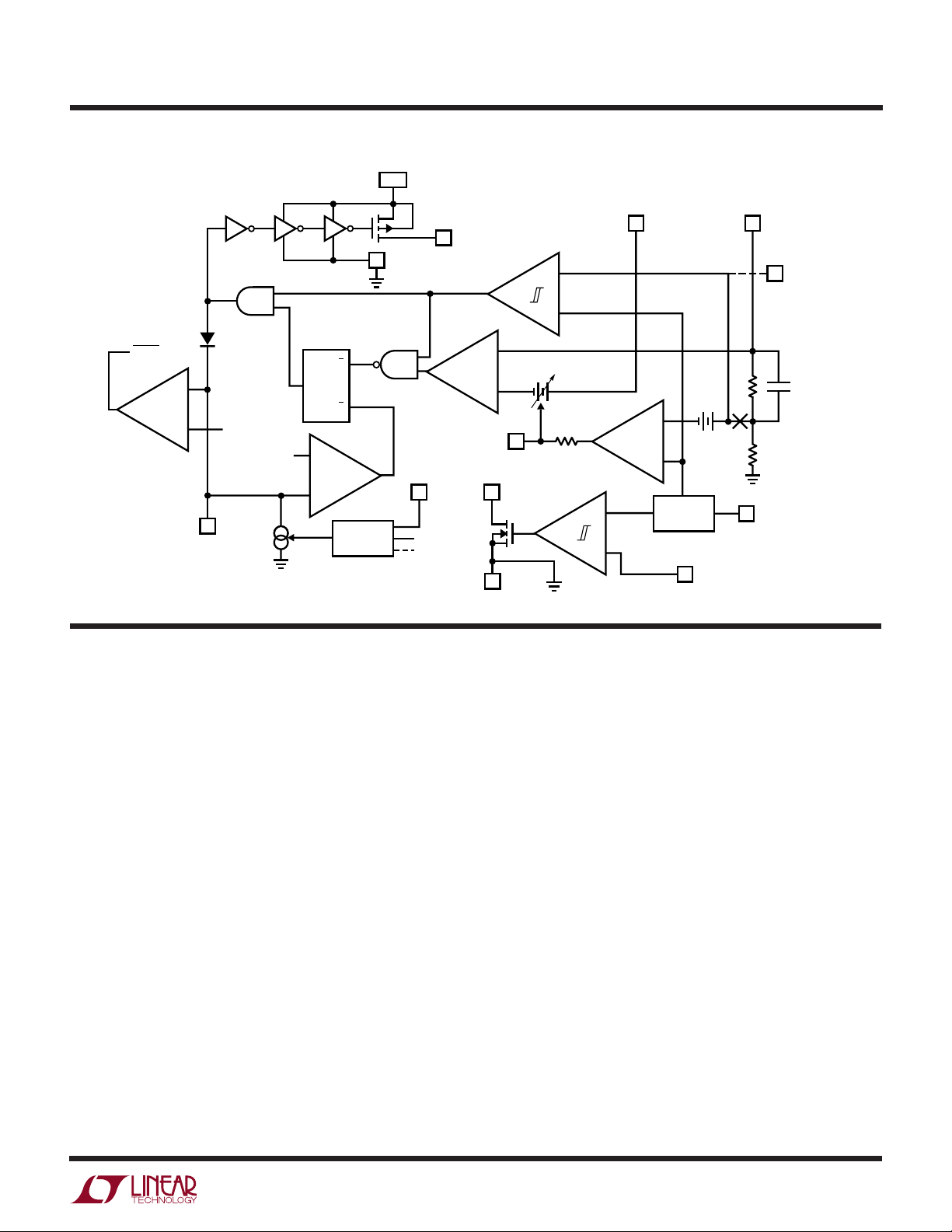
FUNCTIONAL DIAGRA
SLEEP
+
S
–
V
TH2
5
C
T
Q
V
–
TH1
+
(Pin 9 connection shown for LTC1265-3.3 and LTC1265-5; change create LTC1265)
PWR V
1, 13
PGND
12
IN
+
SENSE
SW
14
–
V
+
SENSE
78
–
9
V
FB
ADJUSTABLE
VERSION
–
R
S
T
OFF-TIME
CONTROL
V
2 3
IN
–
SENSE
V
FB
C
+
I
TH
LB
11
SGND
25mV TO 150mV
13k
6
0UT
A3
V
OS
–
G
+
+
–
REFERENCE
4
10
SHDN
LB
IN
5pF
100k
1265 FD
U
OPERATION
The LTC1265 uses a constant off-time architecture to
switch its internal P-channel power MOSFET. The off time
is set by an external timing capacitor at CT (Pin 5). The
operating frequency is then determined by the off time and
the difference between VIN and V
The output voltage is set by an internal resistive divider
(LTC1265-3.3 and LTC1265-5) connected to SENSE
(Pin 7) or an external divider returned to VFB (Pin 9 for
LTC1265). A voltage comparator V, and a gain block G,
compare the divided output voltage with a reference
voltage of 1.25V.
To optimize efficiency, the LTC1265 automatically switches
between continuous and Burst Mode operation. The voltage comparator is the primary control element when the
device is in Burst Mode operation, while the gain block
controls the output voltage in continuous mode.
When the load is heavy, the LTC1265 is in continuous
operation. During the switch ON time, current comparator
C monitors the voltage between Pins 7 and 8 connected
across an external shunt in series with the inductor. When
(Refer to Functional Diagram)
.
OUT
–
the voltage across the shunt reaches the comparator’s
threshold value, its output signal will change state, setting
the flip flop and turning the internal P-channel MOSFET off.
The timing capacitor connected to Pin 5 is now allowed to
discharge at a rate determined by the off-time controller.
When the voltage on the timing capacitor has discharged
past V
, comparator T trips, sets the flip flop and causes
TH1
the switch to turn on. Also, the timing capacitor is recharged. The inductor current will again ramp up until the
current comparator C trips. The cycle then repeats.
When the load current increases, the output voltage decreases slightly. This causes the output of the gain stage
(Pin 6) to increase the current comparator threshold, thus
tracking the load current.
When the load is relatively light, the LTC1265 automatically goes into Burst Mode operation. The current loop is
interrupted when the output voltage exceeds the desired
regulated value. The hysteretic voltage comparator V trips
when V
is above the desired output voltage, shutting
OUT
off the switch and causing the capacitor to discharge. This
5
Page 6

LTC1265/LTC1265-3.3/LTC1265-5
U
OPERATION
(Refer to Functional Diagram)
capacitor discharges past V
below V
. Comparator S then trips and a sleep signal is
TH2
until its voltage drops
TH1
generated. The circuit now enters into sleep mode with the
power MOSFET turned off. In sleep mode, the LTC1265 is
in standby and the load current is supplied by the output
capacitor. All unused circuitry is shut off, reducing quiescent current from 2mA to 160µA. When the output capaci-
tor discharges by the amount of the hysteresis of the
comparator V, the P-channel switch turns on again and the
process repeats itself. During Burst Mode operation the
peak inductor current is set at 25mV/R
U
.
SENSE
WUU
APPLICATIONS INFORMATION
The basic LTC1265 application circuit is shown in
Figure 1. External component selection is driven by the
load requirement, and begins with the selection of R
Once R
is known, CT and L can be chosen. Next, the
SENSE
Schottky diode D1 is selected followed by CIN and C
SENSE
OUT
.
.
To avoid the operation of the current loop interfering with
Burst Mode operation, a built-in offset VOS is incorporated
in the gain stage. This prevents the current from increasing until the output voltage has dropped below a minimum
threshold.
Using constant off-time architecture, the operating frequency is a function of the voltage. To minimize the
frequency variation as dropout is approached, the off-time
controller increases the discharge current as VIN drops
below V
+ 2V. In dropout the P-channel MOSFET is
OUT
turned on continuously (100% duty cycle) providing low
dropout operation with V
I
OUT(MAX)
137.5mV
=
R
SENSE
150mV
=
R
(Amps)
SENSE
OUT
–
≅ VIN.
25mV
2 • R
(Amps)
SENSE
R
R
Selection for Output Current
SENSE
is chosen based on the required output current.
SENSE
With the current comparator monitoring the voltage developed across R
, the threshold of the comparator
SENSE
determines the peak inductor current. Depending on the
load current condition, the threshold of the comparator
lies between 25mV/R
and 150mV/R
SENSE
SENSE
. The maxi-
mum output current of the LTC1265 is:
I
OUT(MAX)
where I
150mV
=
R
SENSE
is the peak-to-peak inductor ripple current.
RIPPLE
–
I
RIPPLE
2
(Amps)
At a relatively light load, the LTC1265 is in Burst Mode
operation. In this mode the peak inductor current is set at
25mV/R
. To fully benefit from Burst Mode operation,
SENSE
the inductor current should be continuous during burst
periods. Hence, the peak-to-peak inductor ripple current
must not exceed 25mV/R
To account for light and heavy load conditions, the I
SENSE
.
OUT(MAX)
is then given by:
Solving for R
and allowing a margin of variations in
SENSE
the LTC1265 and extended component values yields:
R
SENSE
=
I
OUT(MAX)
100mV
(Ω)
The LTC1265 is rated with a capability to supply a maximum
of 1.2A of output current.
R
R
that can be used is 0.083Ω.
SENSE
versus maximum output is given in Figure 2.
SENSE
0.5
0.4
0.3
(Ω)
SENSE
R
0.2
0.1
0
0
MAXIMUM OUTPUT CURRENT (A)
Figure 2. Selecting R
Therefore, the minimum value of
A graph for selecting
0.2
0.4
0.6
0.8
SENSE
1
1265 G10
6
Page 7

LTC1265/LTC1265-3.3/LTC1265-5
U
WUU
APPLICATIONS INFORMATION
Under short-circuit condition, the peak inductor current is
determined by:
I
SC(PK)
In this condition, the LTC1265 automatically extends the
off time of the P-channel MOSFET to allow the inductor
current to decay far enough to prevent any current buildup. The resulting ripple current causes the average shortcircuit current to be approximately I
CT and L Selection for Operating Frequency
The LTC1265 uses a constant off-time architecture with
t
determined by an external capacitor CT. Each time the
OFF
P-channel MOSFET turns on, the voltage on CT is reset to
approximately 3.3V. During the off time, CT is discharged
by a current that is proportional to V
is analogous to the current in inductor L, which likewise,
decays at a rate proportional to V
value must track the timing capacitor value.
The value of CT is calculated from the desired continuous
mode operating frequency:
CT =
where VD is the drop across the Schottky diode.
As the operating frequency is increased, the gate charge
losses will reduce efficiency. The complete expression for
operating frequency is given by:
f ≈
where:
=
1.3(10
1
t
OFF
150mV
R
SENSE
1
4
)f
VIN – V
)
V
IN
VIN – V
)
OUT
+ V
(Amps)
V
+ V
IN
(Hz)
)
D
OUT
D
OUT(MAX)
OUT
. Thus the inductor
OUT
(Farads)
)
.
. The voltage on C
T
2V, the LTC1265 reduces t
current in CT.
dropout. (See shelving effect shown in the Operating
Frequency curve under Typical Performance Characteristics.)
To maintain continuous inductor current at light load, the
inductor must be chosen to provide no more than 25mV/
R
following expression for L:
Using an inductance smaller than the above value will
result in the inductor current being discontinuous. A
consequence of this is that the LTC1265 will delay entering
Burst Mode operation and efficiency will be degraded at
low currents.
Inductor Core Selection
With the value of L selected, the type of inductor must be
chosen. Basically, there are two kinds of losses in an
inductor; core and copper losses.
Core losses are dependent on the peak-to-peak ripple
current and core material. However it is independent of
the physical size of the core. By increasing the inductance, the peak-to-peak inductor ripple current will decrease, therefore reducing core loss. Utilizing low core
loss material, such as molypermalloy or Kool Mµ® will
allow user to concentrate on reducing copper loss and
preventing saturation.
Although higher inductance reduces core loss, it increases copper loss as it requires more windings. When
space is not at a premium, larger wire can be used to
reduce the wire resistance. This also prevents excessive
heat dissipation.
of peak-to-peak ripple current. This results in the
SENSE
L ≥ 5.2(105)R
This prevents audible operation prior to
SENSE(CT)VREG
by increasing the discharge
OFF
V
REG
t
= 1.3(104)C
OFF
V
is the desired output voltage (i.e. 5V, 3.3V). V
REG
the measured output voltage. Thus V
in regulation.
Note that as VIN decreases, the frequency decreases.
When the input-to-output voltage differential drops below
T
)
V
OUT
(sec)
)
REG/VOUT
OUT
= 1
is
CATCH DIODE SELECTION
Losses in the catch diode depend on forward drop and
switching times. Therefore Schottky diodes are a good
choice for low drop and fast switching times.
The catch diode carries load current during the off time.
The average diode current is therefore dependent on the
Kool Mµ is a registered trademark of Magnetics, Inc.
7
Page 8

LTC1265/LTC1265-3.3/LTC1265-5
V
LB_TRIP
= 1.25
1 +
R4
R3
)
)
U
WUU
APPLICATIONS INFORMATION
P-channel switch duty cycle. At high input voltages, the
diode conducts most of the time. As VIN approaches V
the diode conducts only a small fraction of the time. The
most stressful condition for the diode is when the output
is short circuited. Under this condition, the diode must
safely handle I
LTC1265 circuits will be well served by either a 1N5818 or
a MBRS130LT3 Schottky diode. An MBRS0520 is a good
choice for I
C
IN
In continuous mode, the input current of the converter is
a square wave of duty cycle V
voltage transients, a low ESR input capacitor must be
used. In addition, the capacitor must handle a high RMS
current. The CIN RMS current is given by:
I
RMS
This formula has a maximum at VIN = 2V
= I
OUT
design because even significant deviations do not offer
much relief. Note that capacitor manufacturer’s ripple
current ratings are often based on only 2000 hours lifetime. This makes it advisable to further derate the capacitor, or to choose a capacitor rated at a higher temperature
than required. Do not underspecify this component. An
additional 0.1µF ceramic capacitor is also required on
PWR VIN for high frequency decoupling.
C
OUT
The selection of C
resistance (ESR) for proper operation of the LTC1265. The
required ESR of C
ESR
where I
case where the I
of C
OUT
ESR
To avoid overheating, the output capacitor must be sized
to handle the ripple current generated by the inductor. The
OUT(MAX)
I
OUT [VOUT (VIN – VOUT
≈
/2. This simple worst case is commonly used for
< 50mV/I
COUT
is the ripple current of the inductor. For the
RIPPLE
is:
< 2(R
COUT
at close to 100% duty cycle. Most
SC(PK)
≤ 500mA.
OUT/VIN
V
IN
is based upon the effective series
OUT
is:
OUT
RIPPLE
is 25mV/R
RIPPLE
)
SENSE
. To prevent large
1
/
2
)]
(A
RMS
, where I
OUT
, the required ESR
SENSE
)
OUT
RMS
,
worst-case RMS ripple current in the output capacitor is
given by:
≈
150mV
2(R
SENSE
(A
)
)
RMS
OUT
is made too small, the
OUT
and can be improved at
SENSE
has been
RIPPLE(P-P)
I
RMS
Generally, once the ESR requirement for C
met, the RMS current rating far exceeds the I
requirement.
ESR is a direct function of the volume of the capacitor.
Manufacturers such as Nichicon, AVX and Sprague should
be considered for high performance capacitors. The
OS-CON semiconductor dielectric capacitor available
from Sanyo has the lowest ESR for its size at a somewhat
higher price.
In surface mount applications, multiple capacitors may
have to be paralleled to meet the capacitance, ESR or RMS
current handling requirement of the application. Aluminum electrolyte and dry tantalum capacitors are both
available in surface mount configurations. In the case of
tantalum, it is critical that the capacitors are both available
in surface mount configuration and are surge tested for
use in switching power supplies. An excellent choice is the
AVX TPS series of surface mount tantalums, available in
case heights ranging from 2mm to 4mm. Consult the
manufacturer for other specific recommendations.
When the capacitance of C
output ripple at low frequencies will be large enough to trip
the voltage comparator. This causes Burst Mode operation to be activated when the LTC1265 would normally be
in continuous operation. The effect will be most pronounced with low value of R
higher frequencies with lower values of L.
Low-Battery Detection
The low-battery comparator senses the input voltage
through an external resistive divider. This divided voltage
connects to the (–) input of a voltage comparator (Pin 4)
which is compared with a 1.25V reference voltage. Neglecting Pin 4 bias current, the following expression is
used for setting the trip limit:
8
Page 9

LTC1265/LTC1265-3.3/LTC1265-5
U
WUU
APPLICATIONS INFORMATION
The output, Pin 3, is an N-channel open drain that goes low
when the battery voltage is below the threshold set by R3
and R4. In shutdown, the comparator is disabled and Pin
3 is in a high impedance state.
V
IN
R4
4
R3
Figure 3. Low-Battery Comparator
–
+
1.25V REFERENCE
LTC1265
LTC1265 F03
3
THERMAL CONSIDERATIONS
In a majority of applications, the LTC1265 does not
dissipate much heat due to its high efficiency. However, in
applications where the switching regulator is running at
high duty cycles or the part is in dropout with the switch
turned on continuously (DC), the user will need to do some
thermal analysis. The goal of the thermal analysis is to
determine whether the power dissipated by the regulator
exceeds the maximum junction temperature of the part.
The temperature rise is given by:
TR = P(θJA)
where P is the power dissipated by the regulator and θ
JA
is the thermal resistance from the junction of the die to the
ambient temperature.
The junction temperature is simply given by:
TJ = TR + T
A
LTC1265 ADJUSTABLE APPLICATIONS
The LTC1265 develops a 1.25V reference voltage between
the feedback (Pin 9) terminal and signal ground (see
Figure 4). By selecting resistor R1, a constant current is
caused to flow through R1 and R2 to set overall output
voltage. The regulated output voltage is determined by:
R2
V
OUT
= 1.25
1 +
)
R1
)
For most applications a 30k resistor is suggested for R1.
To prevent stray pickup, a 100pF capacitor is suggested
across R1 located close to the LTC1265.
V
OUT
R2
LTC1265
SGND
11
Figure 4. LTC1265 Adjustable Configuration
9
V
FB
100pF
R1
LTC1265 F04
As an example, consider the LTC1265 is in dropout at an
input voltage of 4V with a load current of 0.5A. From the
Typical Performance Characteristics graph of Switch Resistance, the ON resistance of the P-channel is 0.55Ω.
Therefore power dissipated by the part is:
P = I2(R
For the SO package, the θ
) = 0.1375W
DSON
is 110°C/W.
JA
Therefore the junction temperature of the regulator when
it is operating in ambient temperature of 25°C is:
TJ = 0.1375(110) + 25 = 40.1°C
Remembering that the above junction temperature is
obtained from a R
junction temperature based on a higher R
at 25°C, we need to recalculate the
DSON
DSON
since it
increases with temperature. However, we can safely assume that the actual junction temperature will not exceed
the absolute maximum junction temperature of 125°C.
Now consider the case of a 1A regulator with VIN = 4V and
TA = 65°C. Starting with the same 0.55Ω assumption for
R
, the TJ calculation will yield 125°C. But from the
DSON
graph, this will increase the R
to 0.76Ω, which when
DSON
used in the above calculation yields an actual TJ > 148°C.
Therefore the LTC1265 would be unsuitable for a 4V input,
1A output regulator operating at TA = 65°C.
9
Page 10

LTC1265/LTC1265-3.3/LTC1265-5
U
WUU
APPLICATIONS INFORMATION
Board Layout Checklist
When laying out the printed circuit board, the following
checklist should be used to ensure proper operation of the
LTC1265. These items are also illustrated graphically in
the layout diagram of Figure 5. Check the following in your
layout:
1. Are the signal and power grounds segregated? The
LTC1265 signal ground (Pin 11) must return to the (–)
plate of C
anode of the Schottky diode, and the (–) plate of CIN,
whose leads should be as short as possible.
2. Does the (+) plate of the CIN connect to the power V
(Pins 1,13) as close as possible? This capacitor provides the AC current to the internal P-channel MOSFET
and its driver.
3. Is the input decoupling capacitor (0.1µF) connected
closely between power VIN (Pins 1,13) and power
ground (Pin 12)? This capacitor carries the high frequency peak currents.
. The power ground (Pin 12) returns to the
OUT
IN
4. Is the Schottky diode closely connected between the
power ground (Pin 12) and switch (Pin 14)?
5. Does the LTC1265 SENSE– (Pin 7) connect to a point
close to R
and the (+) plate of C
SENSE
? In adjustable
OUT
applications, the resistive divider, R1 and R2, must be
connected between the (+) plate of C
and signal
OUT
ground.
6. Are the SENSE– and SENSE+ leads routed together with
minimum PC trace spacing? The 1000pF capacitor
between Pins 7 and 8 should be as close as possible to
the LTC1265.
7. Is SHDN (Pin 10) actively pulled to ground during
normal operation? The SHDN pin is high impedance
and must not be allowed to float.
1k
3900pF
PWR V
1000pF
1
2
3
4
5
6
7
V
IN
LB
OUT
LB
IN
C
T
I
TH
SENSE
IN
LTC1265
–
1000pF
SW
PWR V
PGND
SGND
SHDN
N/C (VFB)
SENSE
V
IN
14
13
IN
D1
+
12
11
10
SHDN
9
8
+
OUTPUT DIVIDER REQUIRED
WITH ADJUSTABLE VERSION ONLY
C
IN
R1
R2
0.1µF
C
+
OUT
LTC1265 F05
Figure 5. LTC1265 Layout Diagram (See Board Layout Checklist)
L
R
SENSE
V
OUT
BOLD LINES INDICATE
HIGH PATH CURRENTS
10
Page 11

LTC1265/LTC1265-3.3/LTC1265-5
U
WUU
APPLICATIONS INFORMATION
Troubleshooting Hints
Since efficiency is critical to LTC1265 applications, it is
very important to verify that the circuit is functioning
correctly in both continuous and Burst Mode operation. As
the LTC1265 is highly tolerant of poor layout, the output
voltage will still be regulated. Therefore, monitoring the
output voltage will not tell you whether you have a good or
bad layout. The waveform to monitor is the voltage on the
timing capacitor Pin 5.
In continuous mode the voltage on the CT pin is a sawtooth
with approximately 0.9V
never dip below 2V as shown in Figure 6a.
3.3V
(PIN 5)
T
2.4V
swing. This voltage should
P-P
When the load currents are low (I
LOAD
< I
BURST
) Burst
Mode operation occurs. The voltage on CT pin now falls to
ground for periods of time as shown in Figure 6b. During
this time the LTC1265 is in sleep mode with quiescent
current reduced to 160µA.
The inductor current should also be monitored. If the
circuit is poorly decoupled, the peak inductor current will
be haphazard as in Figure 7a. A well decoupled LTC1265
has a clean inductor current as in Figure 7b.
SLEEP MODE
3.3V
(PIN 5)
T
2.4V
VOLTAGE AT C
0V
TIME
(a) CONTINUOUS MODE OPERATION
(a) POORLY DECOUPLED LTC1265
VOLTAGE AT C
0V
LTC1265 F06a
Figure 6. CT Waveforms
Figure 7. Inductor Waveforms
TIME
(b) Burst Mode OPERATION
(b) WELL DECOUPLED LTC1265
LTC1265 F06b
11
Page 12

LTC1265/LTC1265-3.3/LTC1265-5
LOAD CURRENT (mA)
0.01
70
EFFICIENCY (% )
75
80
85
90
100
0.1 1.0
1265 G11
95
L = DALE LPT4545-220 (22µH)
V
OUT
= 3.3V
C
T
= 100pF
U
WUU
APPLICATIONS INFORMATION
Design Example
As a design example, assume VIN = 5V, V
= 0.8A and f = 250kHz. With this information we can easily
calculate all the important components.
From (1),
R
= 100mV/0.8 = 0.125Ω
SENSE
From (2) and assuming VD = 0.4V,
CT ≅ 100pF
Using (3), the value of the inductor is:
L ≥ 5.2(105)(0.125)(100pF)3.3V = 22µH
For the catch diode, a MBRS130LT3 or 1N5818 will be
sufficient in this application.
CIN will require an RMS current rating of at least 0.4A at
temperature, and C
will require an ESR of (from 5):
OUT
OUT
= 3.3V, I
MAX
V
IN
5V
+
C
IN
V
IN
LTC1265-3.3
PGND
SENSE
SENSE
SGND
IN
SW
22µH
0.125Ω
D1
+
1000pF
–
+
LTC1265 F08
V
3.3V
0.8A
C
OUT
OUT
3900pF
0.1µF
1k
100pF
PWR V
SHDN
I
TH
C
T
Figure 8. Design Example Circuit
ESR
The inductor ripple current is given by:
I
RIPPLE
At light loads the peak inductor current is at:
I
PEAK
Therefore, at load current less than 0.1A the LTC1265 will
be in Burst Mode operation. Figure 8 shows the complete
circuit and Figure 9 shows the efficiency curve with the
above calculated component values.
< 0.25Ω
COUT
V
+ V
=
OUT
)
D
t
OFF
)
L
= 25mV/0.125 = 0.2A
= 0.22A
Figure 9. Design Example Efficiency Curve
12
Page 13

U
TYPICAL APPLICATIONS
V
IN
5V
4
3
270pF
3900pF
AVX TPSD107K010
*
AVX TPSE227K010
**
†
COILCRAFT D03316-473
††
DALE WSL2010-0.1-1%
5
1k
6
7
LTC1265/LTC1265-3.3/LTC1265-5
High Efficiency 5V to 3.3V Converter
2 1, 13
V
IN
LB
IN
LTC1265-3.3
LB
OUT
C
T
I
THR
–
SENSE
1000pF
PWR V
IN
14
SW
12
PGND
11
SGND
10
SHDN SHDN
9
NC
8
+
SENSE
+
0.1µF
C
*
IN
100µF
10V
†
L1
47µH
MBRS130LT1
R
SENSE
0.1Ω
††
LTC1265 TA02
V
OUT
C
OUT
220µF
10V
3.3V
**
1A
+
AVX TPSD226K025
*
AVX TPSD107K010
**
†
L1 SELECTION
MANUFACTURER
COILCRAFT
COILTRONICS
DALE
SUMIDA
††
IRC LRC2010-01-R100-J
D1
= MBRS130LT3
VIN (V)
I
3.5
4.0
5.0
6.0
7.0
7.5
OUT(MAX)
360
430
540
630
720
740
PART NO.
DO3316-473
CTX50-4
LPT4545-500LA
CD74-470
(mA)
Positive-to-Negative (–5V) Converter
V
220pF
2200pF
IN
2 1, 13
V
PWR V
IN
4
LB
IN
LTC1265-5
3
LB
OUT
5
C
T
1k
6
I
THR
7
SENSE
1000pF
IN
SW
PGND
SGND
SHDN
SENSE
+
–
3.5V TO 7.5V
TP0610L
14
12
11
10
8
100k
SHDN
D1
L1
50µH
C
*
IN
+
†
R
SENSE
0.1Ω
0.1µF
††
22µF
25V
× 2
V
OUT
–5V
C
OUT
100µF
+
10V
LTC1265 TA03
**
13
Page 14

LTC1265/LTC1265-3.3/LTC1265-5
U
TYPICAL APPLICATIONS
5V Buck-Boost Converter
V
75pF
3300pF
IN
1k
4
3
5
6
7
LB
LB
C
I
THR
SENSE
2 1, 13
V
PWR V
IN
IN
LTC1265
OUT
T
–
0.01µF
IN
SW
PGND
SGND
SHDN SHDN
V
FB
+
SENSE
(V)
V
IN
3.5
4.0
5.0
6.0
7.0
7.5
L1B
3
TOP VIEW
4
L1B
SANYO OS-CON CAPACITOR
*
IRC LRC2010-01-R162-J
**
†
L1A, L2A SELECTION
MANUFACTURER
COILTRONICS
DALE
I
OUT(MAX)
240
275
365
490
610
665
(mA)
L1A
2
•
1
L1A
PART NO.
CTX33-4
LPT4545-330LA
3.5V TO 7.5V
*
C
+
IN
4
3
•
33µF
10V*
††
L1B
33µH
R
SENSE
0.162Ω
+
**
0.1µF
14
12
11
10
9
8
100µF
16V
L1A
33µH
1
1N5818
•
100pF
††
V
OUT
2
75k
25k
5V
+
C
*
OUT
100µF
10V
LTC1265 F09
V
(V)
I
IN
OUT(MAX)
4.0
40
5.0
60
6.0
80
7.0
100
8.0
115
9.0
130
10.0
150
11.0
165
12.0
180
L1B
3
TOP VIEW
4
L1B
AVX TPSE686K020
*
AVX TPSE336K025
**
†
IRC LRC2010-01-R162-J
††
L1A,L2A SELECTION
MANUFACTURER
COILTRONICS
DALE
(mA)
L1A
2
•
1
L1A
PART NO.
CTX50-4
LPT4545-500LA
4V TO 12V
75pF
3300pF
9V to 12V and – 12V Outputs
MBRS130LT3
V
IN
+
C
*
2 1, 13
V
PWR V
IN
4
LB
IN
LTC1265
3
LB
OUT
5
C
T
1k
6
I
THR
7
SENSE
0.01µF
SW
PGND
SGND
SHDN SHDN
V
–
SENSE
IN
FB
+
0.1µF
1N914
14
12
11
10
9
8
IN
68µF
20V
SI19430DY
33µF**
4
•
3
25V
††
L1B
50µH
R
SENSE
0.162Ω
+
*
††
L1A
50µH
•
1
MBRS130LT3
100pF
2
301k
+
34k
LTC1265 TA05
+
C
68µF
20V
OUT
*
C
OUT
68µF
20V
V
12V
OUT
*
V
OUT
–12V
14
Page 15

U
TYPICAL APPLICATIONS
V
51pF
3300pF
IN
4
3
5
1k
6
7
3.5V TO 12.5V
LTC1265/LTC1265-3.3/LTC1265-5
2.5mm Max Height 5V-to-3.3V (500mA)
2 1, 13
V
IN
LB
IN
LTC1265-3.3
LB
OUT
C
T
I
THR
–
SENSE
1000pF
PWR V
IN
14
SW
12
PGND
11
SGND
10
SHDN SHDN
9
N/C
8
+
SENSE
0.1µF
*
C
+
IN
15µF
10V × 2
**
MBRS0520LT1
AVX TAJB156K010
*
AVX TAJB226K06
†
IRC LRC2010-01-R200-J
††
SUMIDA CLS62-180
††
L1
18µH
†
R
SENSE
0.20Ω
LTC1265 TA06
C
OUT
22µF
+
6.3V × 2
**
V
OUT
3.3V
500mA
0V: V
5V: V
75pF
3300pF
OUT
OUT
V
= 5V
= 3.3V
3.5V TO 12.5V
Logic Selectable 0V/3.3V/5V 700mA Regulator
DALE 593D68X0020E2W
*
DALE 593D107X0010D2W
**
†
IRC LRC2010-01-R15-J
††
L1 SELECTION
56.2k
PART NO.
DO3316-333
CTX33-4
LPT4545-330LA
CD74-330
= 3.3V/5V
OUT
= 0V
OUT
45.3k
75k
LTC1265 TA07
**
C
OUT
100µF
+
10V
V
OUT
0V/3.3V/5V
700mA
MANUFACTURER
COILCRAFT
IN
1k
21, 13
V
PWR V
IN
4
LB
IN
LTC1265
3
LB
OUT
5
C
T
6
I
THR
7
SENSE
–
1000pF
IN
SW
PGND
SGND
SHDN V
V
FB
+
SENSE
0.1µF
14
12
11
10
†††
SHDN
9
8
C
*
+
IN
68µF
20V
MBRS130LT3
100pF
COILTRONICS
DALE
SUMIDA
†††
V
= 0V: V
SHDN
= 5V: V
††
L1
33µH
†
R
SENSE
0.15Ω
Information furnished by Linear Technology Corporation is believed to be accurate and reliable.
However, no responsibility is assumed for its use. Linear Technology Corporation makes no representation that the interconnection of its circuits as described herein will not infringe on existing patent rights.
15
Page 16

LTC1265/LTC1265-3.3/LTC1265-5
U
TYPICAL APPLICATIONS
4-NiCad Battery Charger
V
IN
FAST CHARGE: = 0V
TRICKLE CHARGE: > 2V
VN2222L
8V TO 12.5V
51Ω
270pF
1k
3300pF
4
3
5
6
7
LB
LB
C
I
THR
SENSE
2 1, 13
V
PWR V
IN
IN
LTC1265
OUT
T
–
SENSE
1000pF
SW
PGND
SGND
SHDN
V
IN
FB
+
0.1µF
14
12
11
10
CHARGER
ON/OFF
9
8
+
C
*
IN
22µF, 25V
MBRS130LT3
100pF
R
SENSE
0.10Ω
DALE 593D226X0025D2W
*
DALE 593D107X0016E2W
**
†
DALE WSL2010-0.10-1%
††
L1 SELECTION
MANUFACTURER
COILCRAFT
COILTRONICS
SUMIDA
††
L1
100µH
†
30k
138k
PART NO.
DO3316-104
CTX100-4P
CD105-101
**
C
OUT
100µF
+
10V
MBRS130LT3
LTC1265 TA08
V
OUT
4 NICAD
1A FAST CHARGE
0.1A TRICKLE CHARGE
U
PACKAGE DESCRIPTION
0.010 – 0.020
(0.254 – 0.508)
0.008 – 0.010
(0.203 – 0.254)
DIMENSION DOES NOT INCLUDE MOLD FLASH. MOLD FLASH SHALL NOT EXCEED 0.006" (0.152mm) PER SIDE
*
DIMENSION DOES NOT INCLUDE INTERLEAD FLASH. INTERLEAD FLASH SHALL NOT EXCEED 0.010" (0.254mm) PER SIDE
**
× 45°
0.016 – 0.050
(0.406 – 1.270)
0° – 8° TYP
0.053 – 0.069
(1.346 – 1.752)
0.014 – 0.019
(0.355 – 0.483)
TYP
Dimension in inches (millimeters) unless otherwise noted.
0.337 – 0.344*
(8.560 – 8.738)
13
12
11
3
4
0.050
(1.270)
BSC
0.004 – 0.010
(0.101 – 0.254)
(5.791 – 6.197)
0.228 – 0.244
14
1
2
10
5
RELATED PARTS
PART NUMBER DESCRIPTION COMMENTS
LTC1143 Dual Step-Down Switching Regulator Controller Dual Version of LTC1147
LTC1147 Step-Down Switching Regulator Controller Nonsynchronous, 8-Pin, VIN ≤ 16V
LTC1148HV Step-Down Switching Regulator Controller Synchronous, VIN ≤ 20V
LTC1174 Step-Down Switching Regulator with Internal 0.5A Switch VIN ≤ 18.5V, Comparator/Low Battery Detector
LTC1474/LTC1475 Low Quiescent Current Step-Down Regulators Monolithic, IQ = 40µA, 400mA, MS8
LTC1574 Step-Down Switching Regulator with Internal 0.5A Switch VIN ≤ 18.5V, Comparator
and Schottky Diode
LTC1622 Low Input Voltage Step-Down DC/DC Controller Constant Frequency, 2V to 10V VIN, MS8
LTC1627 Monolithic Synchronous Step-Down Switching Regulator Constant Frequency, I
LTC1772 Constant Frequency Step-Down DC/DC Controller SOT-23, 2.2V to 9.8V V
to 500mA, 2.65V to 8.5V V
OUT
IN
9
6
IN
8
0.150 – 0.157**
(3.810 – 3.988)
7
S14 1298
16
Linear Technology Corporation
1630 McCarthy Blvd., Milpitas, CA 95035-7417
(408) 432-1900 ● FAX: (408) 434-0507
●
www.linear-tech.com
126535fa LT/TP 1299 2K REV A • PRINTED IN USA
LINEAR TECHNOLOGY CORPORATION 1995
 Loading...