

Page 1
FEATURES
■
Regulated Negative Voltage from a
Single Positive Supply
■
REG Pin Indicates Output is in Regulation
■
Adjustable or Fixed Output Voltages
■
Output Regulation: ±3.5%
■
Supply Current: 650µA Typ
■
Shutdown Mode Drops Supply Current to 5µA
■
Up to 20mA Output Current
■
Requires Only Three or Four External Capacitors
■
Available in MS8 and SO-8 Packages
U
APPLICATIO S
■
GaAs FET Bias Generators
■
Negative Supply Generators
■
Battery-Powered Systems
■
Single Supply Applications
LTC1261L
Switched Capacitor
Regulated Voltage Inverter
U
DESCRIPTIO
The LTC®1261L is a switched-capacitor voltage inverter
designed to provide a regulated negative voltage from a
single positive supply. The LTC1261L operates from a
single 2.7V to 5.25V supply and provides an adjustable
output voltage from –1.23V to –5V. The LTC1261L-4/
LTC1261L-4.5 needs a single 4.5V to 5.25V supply and
provides a fixed output voltage of –4V to – 4.5V respectively. Three external capacitors are required: a 0.1µF
flying capacitor and an input and output bypass capacitors. An optional compensation capacitor at ADJ (COMP)
can be used to reduce the output voltage ripple.
Each version of the LTC1261L will supply up to 20mA
output current with guaranteed output regulation of ±3.5%.
The LTC1261L includes an open-drain REG output that
pulls low when the output is within 5% of the set value.
Quiescent current is typically 650µA when operating and
5µA in shutdown.
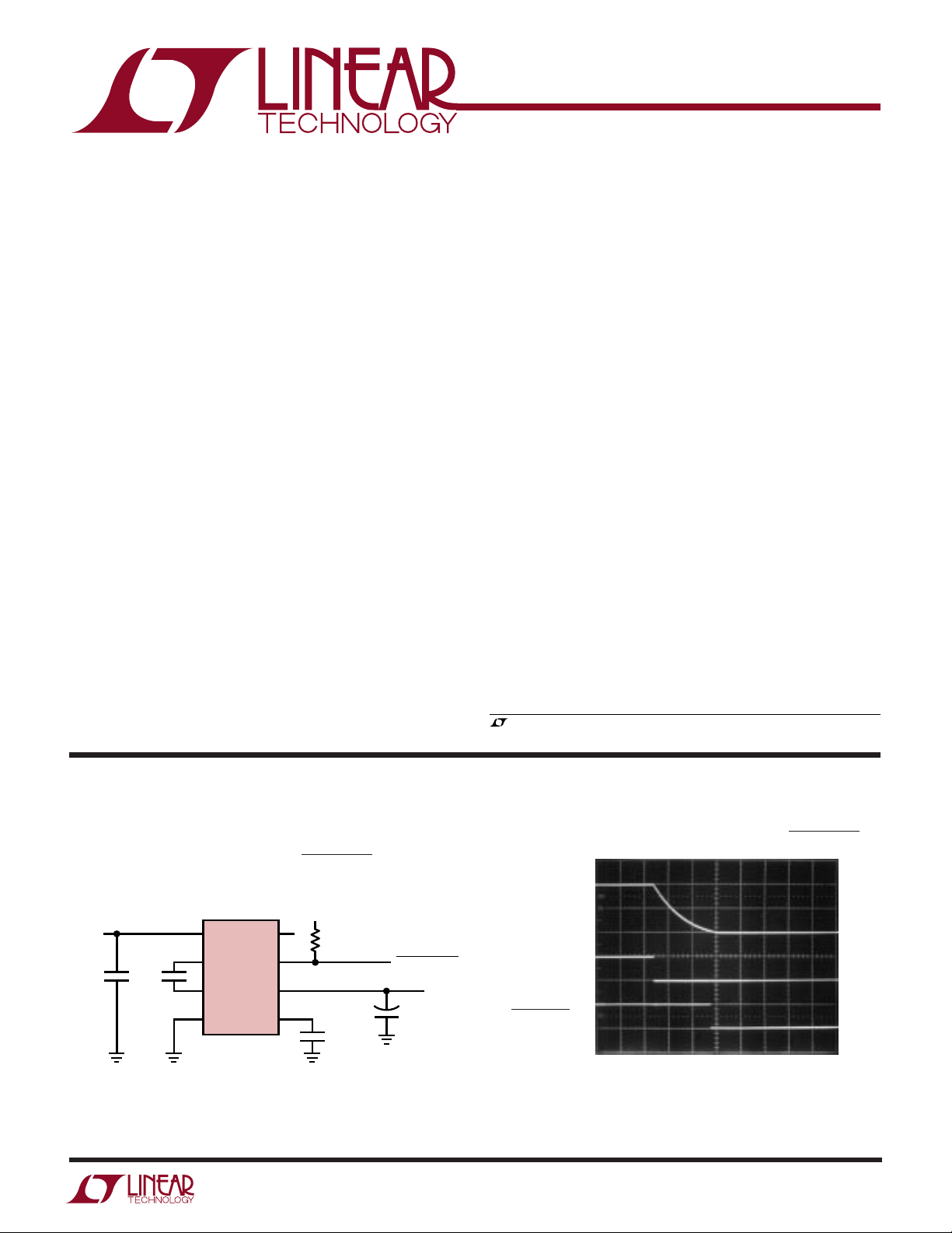
TYPICAL APPLICATION
–4V Generator with Power Valid
5V
C1
1µF
0.1µF
1
V
CC
2
+
C2
C1
3
C1
4
GND
LTC1261L-4
–
SHDN
REG
OUT
COMP
8
7
6
5
The LTC1261L is available in 8-pin MSOP and SO packages.
, LTC and LT are registered trademarks of Linear Technology Corporation.
U
Waveforms for –4V Generator with Power Valid
0V
5V
10k
POWER VALID
V
= –4V
OUT
AT 10mA
C4
3.3µF
C3*
100pF
+
*OPTIONAL
1261L TA01
OUT
SHDN
POWER VALID
–4V
5V
0V
5V
0V
0.1ms/DIV
1261L TAO2
1
Page 2
LTC1261L
A
W
O
LUTEXI TIS
S
A
WUW
U
ARB
G
(Note 1)
Supply Voltage (Note 2) ........................................ 5.5V
Output Voltage (Note 3)........................... 0.3V to –5.3V
Total Voltage, VCC to V
(Note 2) ..................... 10.8V
OUT
SHDN Pin .................................. –0.3V to (VCC + 0.3V)
REG Pin ..................................................... –0.3V to 6V
ADJ Pin........................... (V
– 0.3V) to (VCC + 0.3V)
OUT
WU
/
PACKAGE
V
1
CC
+
2
C1
–
3
C1
4
GND
8-LEAD PLASTIC MSOP
T
JMAX
O
TOP VIEW
MS8 PACKAGE
= 150°C, θ
JA
RDER I FOR ATIO
ORDER PART
NUMBER
8
SHDN
7
REG
6
OUT
5
ADJ (COMP)
= 200°C/W
LTC1261LCMS8
LTC1261LCMS8-4
LTC1261LCMS8-4.5
MS8 PART MARKING
LTFM
LTFN
LTFP
Output Short-Circuit Duration......................... Indefinite
Commercial Temperature Range ................ 0°C to 70°C
Extended Commercial Operating
Temperature Range (Note 4) ................. – 40°C to 85°C
Storage Temperature Range ................ –65°C to 150°C
Lead Temperature (Soldering, 10 sec)................. 300°C
U
ORDER PART
NUMBER
LTC1261LCS8
LTC1261LCS8-4
LTC1261LCS8-4.5
S8 PART MARKING
1261L
1261L4
261L45
V
1
CC
+
C1
2
–
C1
3
GND
4
8-LEAD PLASTIC SO
T
= 150°C, θ
JMAX
TOP VIEW
S8 PACKAGE
JA
8
7
6
5
= 135°C/W
SHDN
REG
OUT
ADJ (COMP)
Consult factory for Industrial or Military grade parts or additional fixed voltage parts.
LECTRICAL C CHARA TERIST
E
temperature range, otherwise specifications are at TA = 25°C, C1 = 0.1µF, C
SYMBOL PARAMETER CONDITIONS MIN TYP MAX UNITS
V
V
I
f
V
I
I
V
V
I
t
CC
REF
CC
OSC
OL
REG
ADJ
IH
IL
IN
ON
Supply Voltage
(LTC1261LCMS8/LTC1261LCS8)
(LTC1261LCMS8-4/LTC1261LCS8-4) (Note 5)
(LTC1261LCMS8-4.5/LTC1261LCS8-4.5) (Note 5)
Reference Voltage 1.23 V
Supply Current VCC = 5.25V, No Load, SHDN Floating ● 650 1500 µA
V
CC
Internal Oscillator Frequency VCC = 5V, V
REG Output Low Voltage I
REG Sink Current V
Adjust Pin Current V
SHDN Input High Voltage VCC = 5V ● 2V
SHDN Input Low Voltage VCC = 5V ● 0.8 V
SHDN Input Current V
Turn-On Time VCC = 5V, I
REG
REG
V
REG
ADJ
SHDN
V
CC
V
CC
VCC = 5V, I
The ● denotes the specifications which apply over the full operating
ICS
= 3.3µF unless otherwise noted. (Notes 2, 4)
OUT
● 2.7 5.25 V
● 4.35 5.25 V
● 4.75 5.25 V
= 5.25V, No Load, V
= –4V 650 kHz
OUT
= 1mA, VCC = 5V, V
= 0.8V, VCC = 3.3V ● 48 mA
= 0.8V, VCC = 5V ● 512 mA
= 1.23V ● ±0.01 ±1 µA
= V
CC
= 10mA, –1.5V ≤V
OUT
= 5V, I
= 5V, I
= 5mA, V
OUT
= 10mA, V
OUT
= 5mA, V
OUT
= V
SHDN
OUT
OUT
OUT
CC
= –4V ● 0.1 0.8 V
≤ –4V (LTC1261L) ● 250 1500 µs
OUT
= –4.5V (LTC1261L) ● 250 1500 µs
= –4V (LTC1261L-4) ● 250 1500 µs
OUT
= –4.5V (LTC1261L-4.5) ● 250 1500 µs
● 520 µA
● 2.5 25 µA
2
Page 3
LTC1261L
LECTRICAL C CHARA TERIST
E
temperature range, otherwise specifications are at TA = 25°C, C1 = 0.1µF, C
The ● denotes the specifications which apply over the full operating
ICS
= 3.3µF unless otherwise noted. (Notes 2, 4)
OUT
SYMBOL PARAMETER CONDITIONS MIN TYP MAX UNITS
V
OUT
I
SC
Note 1: The Absolute Maximum Ratings are those values beyond which
the life of a device may be impaired.
Note 2: All currents into device pins are positive; all currents out of device
pins are negative. All voltages are referenced to ground unless otherwise
specified.
Note 3: The output should never be set to exceed V
Output Regulation (LTC1261L) 2.70V ≤ VCC ≤ 5.25V, 0mA ≤ I
3.25V ≤ V
≤ 5.25V, 0mA ≤ I
CC
2.70V ≤ VCC ≤ 5.25V, 0mA ≤ I
2.95V ≤ V
3.50V ≤ V
≤ 5.25V, 0mA ≤ I
CC
≤ 5.25V, 0mA ≤ I
CC
2.95V ≤ VCC ≤ 5.25V, 0mA ≤ I
3.30V ≤ V
3.85V ≤ V
≤ 5.25V, 0mA ≤ I
CC
≤ 5.25V, 0mA ≤ I
CC
3.40V ≤ VCC ≤ 5.25V, 0mA ≤ I
3.70V ≤ V
4.25V ≤ V
≤ 5.25V, 0mA ≤ I
CC
≤ 5.25V, 0mA ≤ I
CC
3.85V ≤ VCC ≤ 5.25V, 0mA ≤ I
4.10V ≤ V
4.60V ≤ V
≤ 5.25V, 0mA ≤ I
CC
≤ 5.25V, 0mA ≤ I
CC
Output Regulation 4.35V ≤ VCC ≤ 5.25V, 0mA ≤ I
(LTC1261L/LTC1261L-4) 4.60V ≤ V
5.10V ≤ V
≤ 5.25V, 0mA ≤ I
CC
≤ 5.25V, 0mA ≤ I
CC
Output Regulation 4.75V ≤ VCC ≤ 5.25V, 0mA ≤ I
(LTC1261L/LTC1261L-4.5) 5.05V ≤ V
Output Short-Circuit Current V
OUT
≤ 5.25V, 0mA ≤ I
CC
= 0V, VCC = 5.25V ● 100 220 mA
Note 4: The LTC1261L is guaranteed to meet specified performance from
0°C to 70°C and is designed, characterized and expected to meet these
extended commercial temperature limits, but is not tested at –40°C and
85°C. Guaranteed I grade parts are available, consult factory.
Note 5: The LTC1261L-4 and LTC1261L-4.5 will operate with less than the
– 10.8V.
CC
minimum V
not guaranteed to meet the ±3.5% V
≤ 10mA ● –1.552 –1.5 – 1.448 V
OUT
≤ 20mA ● –1.552 –1.5 – 1.448 V
OUT
≤ 5mA ● –2.070 –2.0 – 1.930 V
OUT
≤ 10mA ● –2.070 –2.0 – 1.930 V
OUT
≤ 20mA ● –2.070 –2.0 – 1.930 V
OUT
≤ 5mA ● –2.587 –2.5 – 2.413 V
OUT
≤ 10mA ● –2.587 –2.5 – 2.413 V
OUT
≤ 20mA ● –2.587 –2.5 – 2.413 V
OUT
≤ 5mA ● –3.105 –3.0 – 2.895 V
OUT
≤ 10mA ● –3.105 –3.0 – 2.895 V
OUT
≤ 20mA ● –3.105 –3.0 – 2.895 V
OUT
≤ 5mA ● –3.622 –3.5 – 3.378 V
OUT
≤ 10mA ● –3.622 –3.5 – 3.378 V
OUT
≤ 20mA ● –3.622 –3.5 – 3.378 V
OUT
≤ 5mA ● –4.140 –4.0 – 3.860 V
OUT
≤ 10mA ● –4.140 –4.0 – 3.860 V
OUT
≤ 20mA ● –4.140 –4.0 – 3.860 V
OUT
≤ 5mA ● –4.657 –4.5 – 4.343 V
OUT
≤ 10mA ● –4.657 –4.5 – 4.343 V
OUT
specified in the electrical characteristics table, but they are
CC
specification.
OUT
W
U
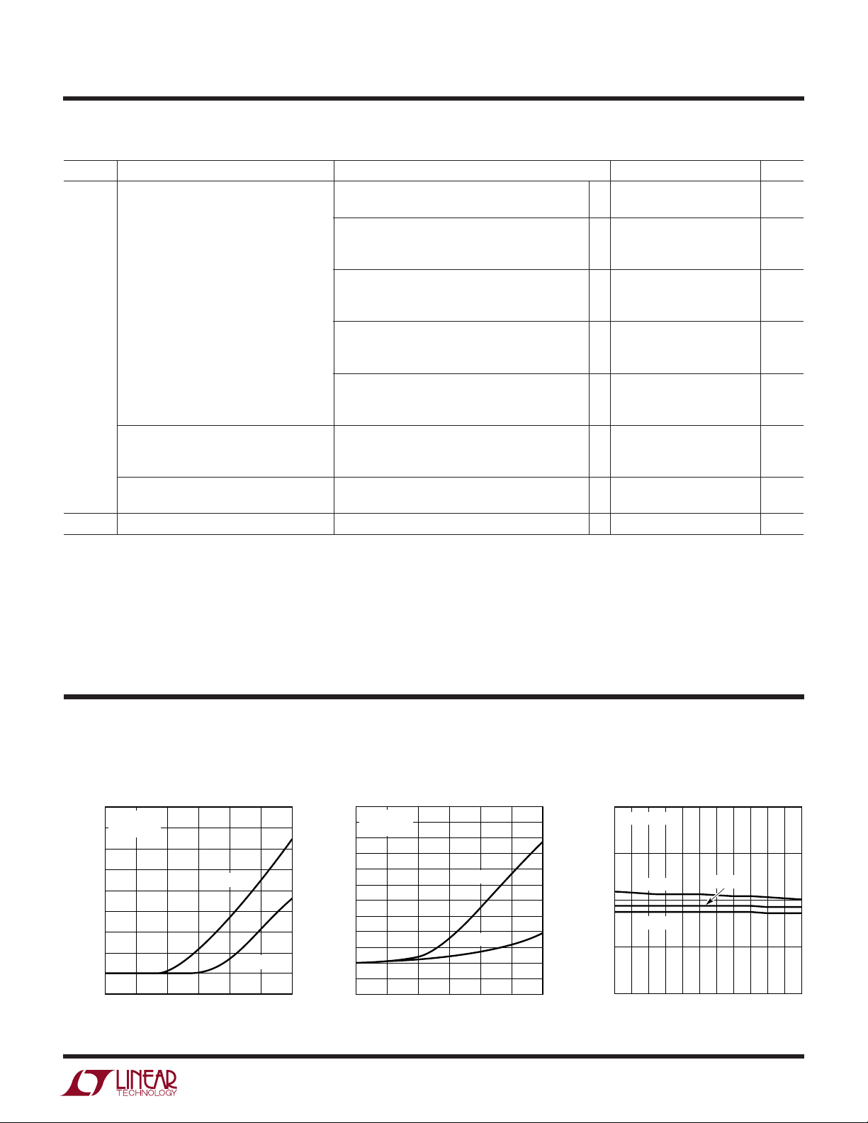
TYPICAL PERFORMANCE CHARACTERISTICS
Output Voltage vs Output Current
0
TA = 25°C
–0.25
–0.50
–0.75
–1.00
–1.25
–1.50
OUTPUT VOLTAGE (V)
–1.75
–2.00
–2.25
= –2V
V
OUT
0
VCC = 2.7V
V
= 3V
CC
1052515 30
OUTPUT CURRENT (mA)
20
1261L G01
–3.0
TA = 25°C
–3.1
V
= –4V
OUT
–3.2
–3.3
–3.4
–3.5
–3.6
–3.7
–3.8
OUTPUT VOLTAGE (V)
–3.9
–4.0
–4.1
–4.2
0
5
OUTPUT CURRENT (mA)
VCC = 4.5V
VCC = 5V
10 15 20
(See Test Circuits)
–1.90
–1.95
–2.00
OUTPUT VOLTAGE (V)
–2.05
25 30
1261L G02
–2.10
Output Voltage vs Supply VoltageOutput Voltage vs Output Current
V
= –2V
OUT
TA = –40°C
T
= 85°C
A
2.5 3.0 3.5 4.0 4.5 5.0
TA = 25°C
SUPPLY VOLTAGE (V)
1261L G03
3
Page 4
LTC1261L
TEMPERATURE (°C)
–55
1.21
REFERENCE VOLTAGE (V)
1.22
1.23
1.24
1.25
–35 –15 5 25
1261L G09
45 65 85 105 125
VCC = 5V
ADJ = 0V
TEMPERATURE (°C)
–40
SHORT-CIRCUIT CURRENT (mA)
80
100
120
80
1261L G12
60
40
0
–10
20
50
–25 95
5
35
65
20
160
140
VCC = 5.25V
VCC = 5V
VCC = 3V
VCC = 2.7V
W
U
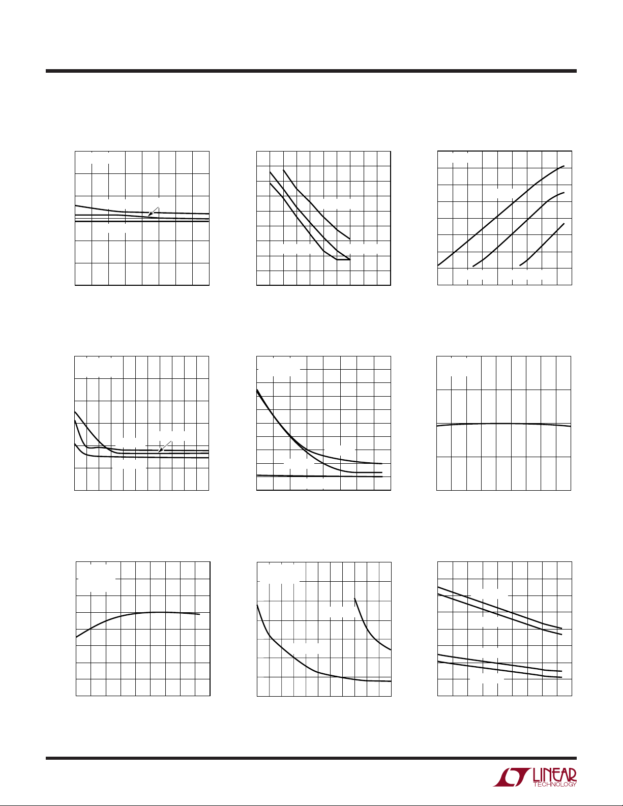
TYPICAL PERFORMANCE CHARACTERISTICS
(See Test Circuits)
Output Voltage vs Supply Voltage
–3.85
V
= –4V
OUT
–3.90
–3.95
–4.00
–4.05
OUTPUT VOLTAGE (V)
–4.10
–4.15
4.5
TA = –40°C
TA = 85°C
4.7 4.9
4.6 4.8
SUPPLY VOLTAGE (V)
TA = 25°C
5.0
Supply Current vs Supply Voltage
3.0
V
= –2V
OUT
= 0
I
OUT
2.5
2.0
1.5
= 85°C
T
1.0
SUPPLY CURRENT (mA)
0.5
0
A
TA = –40°C
3.0 3.5 4.0 4.5
SUPPLY VOLTAGE (V)
5.1
TA = 25°C
5.2
1261L G04
5.02.5
1261L G07
5.3
Minimum Required V
vs V
and I
OUT
5.6
5.2
4.8
4.4
4.0
3.6
3.2
2.8
POSITIVE SUPPLY VOLTAGE (V)
2.4
2.0
–5
5.0
V
= –4.5V
OUT
4.5
I
= 0
OUT
4.0
3.5
3.0
2.5
2.0
1.5
SUPPLY CURRENT (mA)
1.0
0.5
0
4.5
4.6 4.8
OUT
I
OUT
I
= 5mA I
OUT
–4 –3 0
OUTPUT VOLTAGE (V)
T
= 25°C
A
T
= –40°C
A
4.7
4.9
SUPPLY VOLTAGE (V)
CC
= 20mA
OUT
–2 –1
TA = 85°C
5.0
= 10mA
5.1
1261L G05
5.2
1261L G08
5.3
Maximum Output Current
vs Supply Voltage
80
TA = 25°C
70
60
50
40
30
20
MAXIMUM OUTPUT CURRENT (mA)
10
0
2.7
3.0 5.4
V
= –2V
OUT
V
= –3V
OUT
3.3
3.9
3.6
SUPPLY VOLTAGE (V)
V
4.2
Reference Voltage
vs TemperatureSupply Current vs Supply Voltage
OUT
= –4V
4.5
4.8
5.1
1261L G06
Oscillator Frequency
vs Temperature
725
TA = 25°C
V
OUT
700
V
CC
675
650
625
600
575
OSCILLATOR FREQUENCY (kHz)
550
525
–40
–25 95
4
= –4V
= 5V
–10
20
5
TEMPERATURE (°C)
35
Output Short-Circuit Current
vs TemperatureStart-Up Time vs Supply Voltage
0.7
TA = 25°C
= 10mA
I
OUT
0.6
0.5
V
= –4V
= –2V
3.5
OUT
4.0
4.5
5.0
1261L G11
0.4
0.3
0.2
START-UP TIME (ms)
0.1
80
50
65
1261L G10
0
2.5
V
OUT
3.0
SUPPLY VOLTAGE (V)
Page 5

UUU
PIN FUNCTIONS
LTC1261L
VCC (Pin 1): Power Supply. This requires an input voltage
between 2.7V and 5.25V. VCC must be bypassed to
ground with at least a 1µF capacitor placed in close
proximity to the chip. See the Applications Information
section for details.
C1+ (Pin 2):
C1 Positive Input. Connect a 0.1µF capacitor
between C1+ and C1–.
C1– (Pin 3): C1 Negative Input. Connect a 0.1µF capacitor
from C1+ to C1–.
GND (Pin 4): Ground. Connect to a low impedance
ground. A ground plane will help to minimize regulation
errors.
ADJ (COMP for fixed versions) (Pin 5): Output Adjust/
Compensation Pin. For adjustable parts this pin is used
to set the output voltage. The output voltage is divided
down with an external resistor divider and fed back to this
pin to set the regulated output voltage. Typically the
resistor string should draw ≥10µA from the output to
minimize errors due to the bias current at the adjust pin.
Fixed output voltage parts have the internal resistor
string connected to this pin inside the package. The pin
can be used to trim the output voltage if desired. It can
also be used as an optional feedback compensation pin to
reduce output ripple on both the adjustable and fixed
output voltage parts. See the Applications Information
section for more information on compensation and output ripple.
OUT (Pin 6): Negative Voltage Output. This pin must be
bypassed to ground with a 1µF or larger capacitor. The
value of the output capacitor and its ESR have a strong
effect on output ripple. See the Applications Information
section for more details.
REG (Pin 7): This is an open-drain output that pulls low
when the output voltage is within 5% of the set value. It
will sink 5mA to ground with a 5V supply. The external
circuitry must provide a pull-up or REG will not swing
high. The voltage at REG may exceed VCC and can be
pulled up to 6V above ground without damage.
SHDN (Pin 8): Shutdown. When this pin is at ground the
LTC1261L operates normally. An internal 5µA pull-down
keeps SHDN low if it is left floating. When SHDN is pulled
high, the LTC1261L enters shutdown mode. In shutdown, the charge pump is disabled, the output collapses
to 0V and the quiescent current drops to 5µA typically.
TEST CIRCUITS
1
5V
+
10µF
0.1µF
V
2
C1
3
C1
4
GND
CC
+
LTC1261L-X
–
Fixed Output
8
SHDN
7
REG
6
OUT
5
COMP
+
3.3µF
1261L TCO1
V
= –4V (LTC1261L-4)
OUT
= –4.5V (LTC1261L-4.5)
V
OUT
0.1µF
Adjustable Output
1
2
3
4
V
CC
+
C1
LTC1261L
–
C1
GND
V
CC
SHDN
REG
OUT
ADJ
8
7
6
5
+
3.3µF
1261L TCO2
V
OUT
5
Page 6

LTC1261L
U
WUU
APPLICATIONS INFORMATION
The LTC1261L uses an inverting charge pump to generate
a regulated negative output voltage that is either equal to
or less than the supply voltage. The LTC1261L needs only
three external capacitors and is available in the MSOP and
SO-8 packages
THEORY OF OPERATION
A block diagram of the LTC1261L is shown in Figure 1. The
heart of the LTC1261L is the charge pump core shown in
the dashed box. It generates a negative output voltage by
first charging the flying capacitor (C1) between VCC and
ground. It then connects the top of the flying capacitor to
ground, forcing the bottom of the flying capacitor to a
negative voltage. The charge on the flying capacitor is
transferred to the output bypass capacitor, leaving it
charged to the negative output voltage. This process is
driven by the internal 650kHz clock.
Figure 1 shows the charge pump configuration. With the
clock low, C1 is charged to VCC by S1 and S3. At the next
rising clock edge, S1 and S3 are open and S2 and S4
closed. S2 connects C1+ to ground, C1– is connected to
the output by S4. The charge in C1 is transferred to C
OUT
,
setting it to a negative voltage.
The output voltage is monitored by COMP1 which com-
pares a divided replica of the output at ADJ (COMP for
fixed output voltage parts) to the internal reference. At the
beginning of a cycle the clock is low, forcing the output of
the AND gate low and charging the flying capacitor. The
next rising clock edge sets the RS latch, setting the charge
pump to transfer charge from the flying capacitor to the
output capacitor. As long as the output is below the set
point, COMP1 stays low, the latch stays set and the charge
pump runs at the full 50% duty cycle of the clock gated
through the AND gate. As the output approaches the set
voltage, COMP1 will trip whenever the divided signal
exceeds the internal 1.23V reference relative to OUT. This
resets the RS latch and truncates the clock pulses, reducing the amount of charge transferred to the output capacitor and regulating the output voltage. If the output exceeds
the set point, COMP1 stays high, inhibiting the RS latch
and disabling the charge pump.
CLK
650kHz
S
R
V
CC
S1
+
C1
C1
Q
S2
C1
S3
+
COMP1
–
60mV
= 1.23V
V
REF
1.17V
V
OUT
Figure 1. Block Diagram
S4
–
+
COMP2
–
R2
R1
ADJ (COMP)
OUT
REG
C
OUT
+
INTERNALLY
CONNECTED FOR
FIXED OUTPUT
VOLTAGE PARTS
1261L F01
6
Page 7

LTC1261L
U
WUU
APPLICATIONS INFORMATION
COMP2 also monitors the divided signal at ADJ but it is
connected to a 1.17V reference, 5% below the main
reference voltage. When the divided output exceeds this
lower reference voltage indicating that the output is within
5% of the set value, COMP2 goes high turning on the REG
output transistor. This is an open drain N-channel device
capable of sinking 4mA with a 3.3V VCC and 5mA with a 5V
VCC. When in the “off” state (divided output is more than
5% below V
damage up to a maximum of 6V above ground. Note that
the REG output only indicates if the magnitude of the
output is
V
> – 4.75V for a – 5V set point). If the magnitude of the
OUT
output is forced
( i.e., to –5.25V when the output is set for – 5V) the REG
output will stay low.
OUTPUT RIPPLE
Output ripple in the LTC1261L is present from two sources;
voltage droop at the output capacitor between clocks and
frequency response of the regulation loop. Voltage droop
is easy to calculate. With a typical clock frequency of
650kHz, the charge on the output capacitor is refreshed
once every 1.54µs. With a 15mA load and a 3.3µF output
capacitor, the output will droop by:
I
LOAD
)
C
This can be a significant ripple component when the
output is heavily loaded, especially if the output capacitor
is small. If absolute minimum output ripple is required, a
10µF or greater output capacitor should be used.
Regulation loop frequency response is the other major
contributor to output ripple. The LTC1261L regulates the
output voltage by limiting the amount of charge transferred to the output capacitor on a cycle-by-cycle basis.
The output voltage is sensed at the ADJ pin (COMP for
fixed output voltage versions) through an internal or
external resistor divider from the OUT pin to ground. As
the flying capacitor is first connected to the output, the
output voltage begins to change quite rapidly. As soon as
it exceeds the set point COMP1 trips, switching the state
) the drain can be pulled above VCC without
REF
below
the magnitude of the set point by 5% (i.e.,
higher
than the magnitude of the set point
∆t
OUT
= 15mA
)
1.54µs
)
3.3µF
= 7mV
)
of the charge pump and stopping the charge transfer.
Because the RC time constant of the capacitors and the
switches is quite short, the ADJ pin must have a wide AC
bandwidth to be able to respond to the output in time.
External parasitic capacitance at the ADJ pin can reduce
the bandwidth to the point where the comparator cannot
respond by the time the clock pulse finishes. When this
happens the comparator will allow a few complete pulses
through, then overcorrect and disable the charge pump
until the output drops below the set point. Under these
conditions the output will remain in regulation but the
output ripple will increase as the comparator “hunts” for
the correct value.
To prevent this from happening, an external capacitor can
be connected from ADJ (or COMP for fixed output voltage
parts) to ground to compensate for external parasitics and
increase the regulation loop bandwidth (Figure 2). This
sounds counterintuitive until we remember that the internal reference is generated with respect to OUT, not ground.
The feedback loop actually sees ground as its “output,”
thus the compensation capacitor should be connected
across the “top” of the resistor divider, from ADJ (or
COMP) to ground. By the same token, avoid adding
capacitance between ADJ (or COMP) and V
slow down the feedback loop and increase output ripple.
A 100pF capacitor from ADJ or COMP to ground will
compensate the loop properly under most conditions for
fixed voltage versions of the LTC1261L. For the adjustable
LTC1261L, the capacitor value will be dependent upon the
values of the external resistors in the divider network.
TO CHARGE
PUMP
COMP1
REF
+
1.23V
–
Figure 2. Regulator Loop Compensation
RESISTORS ARE
INTERNAL FOR FIXED
OUTPUT VOLTAGE PARTS
R1
ADJ/COMP
R2
V
OUT
1261L F02
. This will
OUT
C
C
100pF
7
Page 8

LTC1261L
U
WUU
APPLICATIONS INFORMATION
OUTPUT FILTERING
If extremely low output ripple (<5mV) is required, additional output filtering is required. Because the LTC1261L
uses a high 650kHz switching frequency, fairly low value
RC or LC networks can be used at the output to effectively
filter the output ripple. A 10Ω series output resistor and a
3.3µF capacitor will cut output ripple to below 3mV (Figure
3). Further reductions can be obtained with larger filter
capacitors or by using an LC output filter.
5V
1µF
0.1µF
Figure 3. Output Filter Cuts Ripple Below 3mV
CAPACITOR SELECTION
2
C1
3
C1
V
CC
+
LTC1261L-4
–
COMP
GND
4
OUT
6
5
100pF
10Ω
1261L F03
3.3µF
+
3.3µF
+
= – 4V
V
OUT
capacitor type for both the input bypass capacitor and the
flying capacitor.
In applications where the maximum load current is welldefined and output ripple is critical or input peak currents
need to be minimized, the flying capacitor value can be
tailored to the application. Reducing the value of the
flying capacitor reduces the amount of charge transferred with each clock cycle. This limits maximum output
current, but also cuts the size of the voltage step at the
output with each clock cycle. The smaller capacitor
draws smaller pulses of current out of VCC as well,
limiting peak currents and reducing the demands on the
input supply. Table 1 shows recommended values of
flying capacitor vs maximum load capacity.
Table 1. Typical Max Load (mA) vs Flying Capacitor Value at
TA = 25°C, V
= –4V
OUT
FLYING
CAPACITOR MAX LOAD (mA)
VALUE (µF) VCC = 5V
0.1 20
0.047 15
0.033 10
0.022 5
0.01 1
Capacitor Sizing
The performance of the LTC1261L is affected by the
capacitors to which it connects. The LTC1261L requires
bypass capacitors to ground for both the VCC and OUT
pins. The input capacitor provides most of LTC1261L’s
supply current while it is charging the flying capacitors.
This capacitor should be mounted as close to the package
as possible and its value should be at least ten times larger
than the flying capacitor. Ceramic capacitors generally
provide adequate performance. Avoid using a tantalum
capacitor as the input bypass unless there is at
least a
0.1µF ceramic capacitor in parallel with it. The charge
pump capacitor is somewhat less critical since its peak
current is limited by the switches inside the LTC1261L.
Most applications should use a 0.1µF as the flying
capacitor value. Conveniently, ceramic capacitors are the
most common type of 0.1µF capacitor and they work well
here. Usually the easiest solution is to use the same
The output capacitor performs two functions: it provides
output current to the load during half of the charge pump
cycle and its value helps to set the output ripple voltage.
For applications that are insensitive to output ripple, the
output bypass capacitor can be as small as 1µF. Larger
output capacitors will reduce output ripple further at the
expense of turn-on time.
Capacitor ESR
Output capacitor Equivalent Series Resistance (ESR) is
another factor to consider. Excessive ESR in the output
capacitor can fool the regulation loop into keeping the
output artificially low by prematurely terminating the charging cycle. As the charge pump switches to recharge the
output a brief surge of current flows from the flying
capacitors to the output capacitor. This current surge can
be as high as 100mA under full load conditions. A typical
8
Page 9

LTC1261L
U
WUU
APPLICATIONS INFORMATION
3.3µF tantalum capacitor has 1Ω or 2Ω of ESR; 100mA ×
2Ω = 200mV. If the output is within 200mV of the set point
this additional 200mV surge will trip the feedback comparator and terminate the charging cycle. The pulse dissipates quickly and the comparator returns to the correct
state, but the RS latch will not allow the charge pump to
respond until the next clock edge. This prevents the charge
pump from going into very high frequency oscillation
under such conditions but it also creates an output error
as the feedback loop regulates based on the top of the
spike, not the average value of the output (Figure 4). The
resulting output voltage behaves as if a resistor of value
C
× (IPK/I
ESR
avoid this nasty sequence of events, connect a 0.1µF
ceramic capacitor in parallel with the larger output capacitor. The ceramic capacitor will “eat” the high frequency
spike, preventing it from fooling the feedback loop, while
the larger but slower tantalum or aluminum output capacitor supplies output current to the load between charge
cycles.
CLOCK
LOW ESR
OUTPUT CAP
HIGH ESR
OUTPUT CAP
Figure 4. Output Ripple with Low and High ESR Capacitors
Note that ESR in the flying capacitor will not cause the
same condition; in fact, it may actually improve the situation by cutting the peak current and lowering the amplitude of the spike. However, more flying capacitor ESR is
not necessarily better. As soon as the RC time constant
)Ω was placed in series with the output. To
AVE
V
SET
V
V
OUT
V
OUT
OUT
AVERAGE
COMP1
OUTPUT
V
SET
V
OUT
AVERAGE
COMP1
OUTPUT
1261L F04
approaches half of a clock period (the time the capacitors
have to share charge at full duty cycle) the output current
capability of the LTC1261L starts to diminish. For a 0.1µF
flying capacitor, this gives a maximum total series resistance of:
t
1
CLK
= /0.1µF = 7.7Ω
)
)
C
2
FLY
1
)
2
650kHz
1
)
Most of this resistance is already provided by the internal
switches in the LTC1261L. More than 1Ω or 2Ω of ESR on
the flying capacitors will start to affect the regulation at
maximum load.
RESISTOR SELECTION
Resistor selection is easy with the fixed output voltage
versions of the LTC1261L—no resistors are needed!
Selecting the right resistors for the adjustable parts is only
a little more difficult. A resistor divider should be used to
divide the signal at the output to give 1.23V at the ADJ pin
with respect to V
positive reference with respect to V
(Figure 5). The LTC1261L uses a
OUT
, not a negative
OUT
reference with respect to ground (Figure 1 shows the
reference connection). Be sure to keep this in mind when
connecting the resistors! If the initial output is not what
you expected, try swapping the two resistors.
The LTC1261L can be internally configured for other
fixed output voltages. Contact the Linear Technology
Marketing department for details.
4
GND
LTC1261L
ADJ
OUT
Figure 5. External Resistor Connections
R1
5
R2
6
V
OUT
= –1.23V
R1 + R2
()
R2
1261L F05
9
Page 10

LTC1261L
U
TYPICAL APPLICATIONS N
5V Input, –4V Output GaAs FET Bias Generator
V
BAT
SHUTDOWN
5V
1µF
0.1µF
1
V
2
C1
3
C2
4
GND
1mV Ripple, 5V Input, –4V Output GaAs FET Bias Generator
SHDN
CC
+
LTC1261L-4
–
COMP
REG
OUT
P-CHANNEL
POWER SWITCH
8
7
6
5
100pF
10k
–4V BIAS
GaAs
3.3µF
+
TRANSMITTER
1261 TA03
5V
1µF
V
BAT
SHUTDOWN
1µF
5V
SHUTDOWN
0.1µF
0.1µF
P-CHANNEL
POWER SWITCH
V
BAT
1
V
2
C1
3
C2
4
GND
SHDN
CC
+
LTC1261L-4
–
COMP
REG
OUT
8
7
6
5
100pF
10k
100µH
10µF
+ +
5V Input, –0.5V Output GaAs FET Bias Generator
P-CHANNEL
POWER SWITCH
1
2
3
4
V
CC
+
C1
LTC1261L
–
C2
GND
SHDN
REG
OUT
ADJ
43.2k
8
7
6
5
1%
100pF
10k
12.4k
1%
–4V BIAS
10µF
–0.5V BIAS
+
3.3µF
GaAs
TRANSMITTER
GaAs
TRANSMITTER
1261 TA04
1261 TA05
10
Page 11

PACKAGE DESCRIPTION
(
U
Dimensions in inches (millimeters) unless otherwise noted.
MS8 Package
8-Lead Plastic MSOP
(LTC DWG # 05-08-1660)
0.118 ± 0.004*
(3.00 ± 0.102)
8
7
6
5
LTC1261L
0.192 ± 0.004
(4.88 ± 0.10)
12
0.040
± 0.006
SEATING
PLANE
(1.02 ± 0.15)
0.012
(0.30)
0.0256
REF
(0.65)
0.152mm) PER SIDE
TYP
0.007
(0.18)
0.021
± 0.006
(0.53 ± 0.015)
* DIMENSION DOES NOT INCLUDE MOLD FLASH, PROTRUSIONS OR GATE BURRS. MOLD FLASH,
PROTRUSIONS OR GATE BURRS SHALL NOT EXCEED 0.006" (0.152mm) PER SIDE
** DIMENSION DOES NOT INCLUDE INTERLEAD FLASH OR PROTRUSIONS.
INTERLEAD FLASH OR PROTRUSIONS SHALL NOT EXCEED 0.006"
° – 6° TYP
0
0.118 ± 0.004**
4
3
0.034 ± 0.004
(0.86 ± 0.102)
(3.00 ± 0.102)
S8 Package
8-Lead Plastic Small Outline (Narrow 0.150)
(LTC DWG # 05-08-1610)
0.189 – 0.197*
(4.801 – 5.004)
7
8
5
6
0.006 ± 0.004
(0.15 ± 0.102)
MSOP (MS8) 1197
0.228 – 0.244
(5.791 – 6.197)
0.010 – 0.020
(0.254 – 0.508)
0.008 – 0.010
(0.203 – 0.254)
*
DIMENSION DOES NOT INCLUDE MOLD FLASH. MOLD FLASH
SHALL NOT EXCEED 0.006" (0.152mm) PER SIDE
**
DIMENSION DOES NOT INCLUDE INTERLEAD FLASH. INTERLEAD
FLASH SHALL NOT EXCEED 0.010" (0.254mm) PER SIDE
Information furnished by Linear Technology Corporation is believed to be accurate and reliable.
However, no responsibility is assumed for its use. Linear Technology Corporation makes no representation that the interconnection of its circuits as described herein will not infringe on existing patent rights.
× 45°
0°– 8° TYP
0.016 – 0.050
0.406 – 1.270
0.053 – 0.069
(1.346 – 1.752)
0.014 – 0.019
(0.355 – 0.483)
0.150 – 0.157**
(3.810 – 3.988)
1
3
2
4
0.004 – 0.010
(0.101 – 0.254)
0.050
(1.270)
TYP
SO8 0996
11
Page 12

LTC1261L
1
2
3
4
8
7
6
5
SHDN
REG
OUT
COMP
V
CC
C1
+
C1
–
GND
0.1µF
1261L TA07
3.3µF
V
OUT
= – 4.5V
AT 5mA
5V
1µF
+
LTC1261L-4.5
U
TYPICAL APPLICATIONS N
Minimum Parts Count –4.5V Generator
1µF
0.1µF
2
3
Low Output Voltage Generator
5V
+
C1
LTC1261L
–
C1
V
GND
1
CC
ADJ
OUT
4
100pF
5
6
1N5817
R
S
124k
= V
OUT
CC
= –0.5V (R
= –1V (R
– 9.92µA (RS + 124k)
= 432k)
S
= 487k)
S
1261L TA06
V
3.3µF
+
RELATED PARTS
PART NUMBER DESCRIPTION COMMENTS
LT1121 Micropower Low Dropout Regulator with Shutdown 0.4V Dropout Voltage at 150mA, Low Noise,
Switched Capacitor Regulated Voltage Inverter
LTC1429 Clock Synchronized Switched Capacitor Regulated Voltage Inverter GaAs FET Bias
LTC1503-1.8/LTC1503-2 High Efficiency Inductorless Step-Down DC/DC Converter Fixed 1.8V or 2V Output from 2.4V to 6V Input,
= 100mA
I
OUT
LTC1514/LTC1515 Step-Up/Step-Down Switched Capacitors DC/DC Converters VIN 2V to 10V, V
LTC1516 Micropower, Regulated 5V Charge Pump DC/DC Converter I
= 20mA (VIN ≥2V), I
OUT
LTC1517-5 Micropower, Regulated 5V Charge Pump DC/DC Converter LTC1522 Without Shutdown and Packaged in SOT-23
LTC1522 Micropower, Regulated 5V Charge Pump DC/DC Converter I
= 10mA (VIN ≥2.7V), I
OUT
LTC1550L/LTC1551L Low Noise Switched Capacitor Regulated Voltage Inverter GaAs FET Bias with Linear Regulator, <1mV Ripple, MSOP
LTC1555/LTC1556 Sim Power Supply and Level Translator Step-Up/Step-Down Sim Power Supply
and Level Translators
LT1611 1.4MHz Inverting Mode Switching Regulator –5V at 150mA from a 5V Input, 5-lead SOT-23
LT1614 Inverting 600kHz Switching Regulator with Low-Battery Detector –5V at 200mA from 5V Input in MSOP
LT1617/LT1617-1 Micropower Inverting DC/DC Converters –15V at 12mA from 2.5V Input, 5-lead SOT-23
LTC1682/LTC1682-3.3/ Low Noise Doubler Charge Pumps Output Noise = 60µV
LTC1682-5
LTC1754-5 Micropower, Regulated 5V Charge Pump with Shutdown in SOT-23 ICC = 13µA, I
(VIN ≥ 2.7V)
is Fixed or Adjustable, I
OUT
= 50mA (VIN ≥3V)
OUT
OUT
, 2.5V to 5.5V Output
RMS
= 50mA (VIN ≥ 3V), I
OUT
OUT
= 20mA (VIN ≥3V)
= 25mA
OUT
up to 50mA
12
Linear Technology Corporation
1630 McCarthy Blvd., Milpitas, CA 95035-7417
(408) 432-1900 ● FAX: (408) 434-0507
●
www.linear-tech.com
1261lf LT/TP 0200 4K • PRINTED IN USA
LINEAR TECHNOLOGY CORPORATION 1999
 Loading...