

Page 1
LTC1250
Very Low Noise
Zero-Drift Bridge Amplifier
EATU
F
■
Very Low Noise: 0.75µV
■
DC to 1Hz Noise Lower Than OP-07
■
Full Output Swing into 1k Load
■
Offset Voltage: 10µV Max
■
Offset Voltage Drift: 50nV/°C Max
■
Common-Mode Rejection Ratio: 110dB Min
■
Power Supply Rejection Ratio: 115dB Min
■
No External Components Required
■
Pin-Compatible with Standard 8-Pin Op Amps
PPLICATI
A
■
Electronic Scales
■
Strain Gauge Amplifiers
■
Thermocouple Amplifiers
■
High Resolution Data Acquisition
■
Low Noise Transducers
■
Instrumentation Amplifiers
RE
S
O
U
S
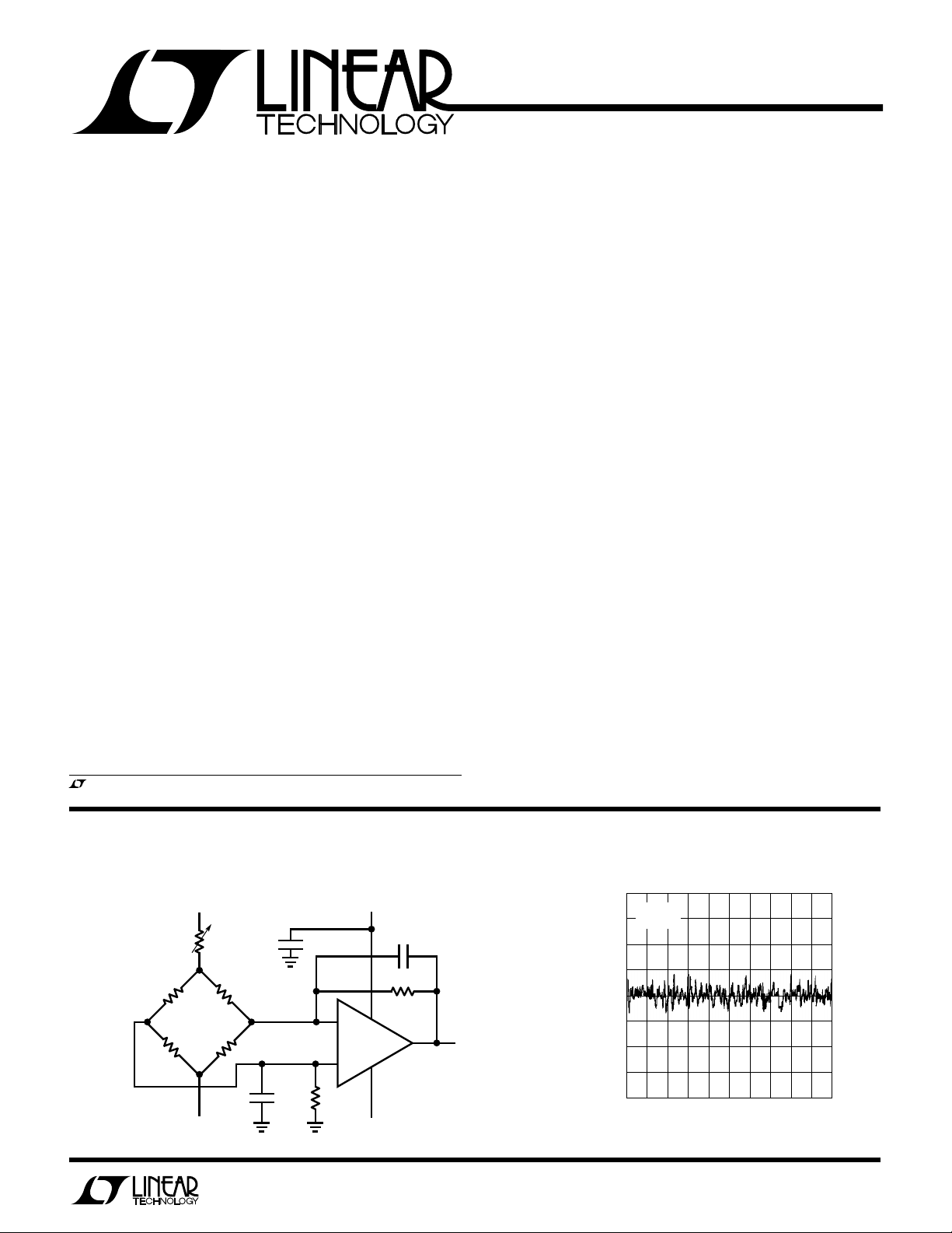
Typ, 0.1Hz to 10Hz
P-P
DUESCRIPTIO
The LTC®1250 is a high performance, very low noise zerodrift operational amplifier. The LTC1250’s combination of
low front-end noise and DC precision makes it ideal for use
with low impedance bridge transducers. The LTC1250
features typical input noise of 0.75µV
10Hz, and 0.2µ V
DC to 1Hz noise of 0.35µ V
from 0.1Hz to 1Hz. The LTC1250 has
P-P
, surpassing that of low noise
P-P
bipolar parts including the OP-07, OP-77, and LT1012.
The LTC1250 uses the industry-standard single op amp
pinout, and requires no external components or nulling
signals, allowing it to be a plug-in replacement for bipolar
op amps.
The LTC1250 incorporates an improved output stage
capable of driving 4.3V into a 1k load with a single 5V
supply; it will swing ±4.9V into 5k with ±5V supplies. The
input common mode range includes ground with single
power supply voltages above 12V. Supply current is 3mA
with a ±5V supply, and overload recovery times from
positive and negative saturation are 0.5ms and 1.5ms,
respectively. The internal nulling clock is set at 5kHz for
optimum low frequency noise and offset drift; no external
connections are necessary.
from 0.1Hz to
P-P
and LTC are registered trademarks and LT is a trademark of Linear Technology Corporation.
U
O
A
PPLICATITYPICAL
Differential Bridge Amplifier
2
3
18.2k
–
LTC1250
+
5V
1000pF
18.2k
7
6
4
–5V
5V
350Ω
STRAIN
GAUGE
–5V
50Ω
GAIN
TRIM
0.1µF
1000pF
The LTC1250 is available in standard 8-pin ceramic and
plastic DIPs, as well as an 8-pin SOIC package.
Input Referred Noise 0.1Hz to 10Hz
2
VS = ±5V
= 10k
A
V
1
0
µV
A
= 100
V
1250 TA01
–2
–1
2
0
4
TIME (s)
6
8
10
LT1250 TA02
1
Page 2
LTC1250
W
O
A
LUTEXI T
S
Total Supply Voltage (V+ to V–) ............................. 18V
Input Voltage ........................ (V+ + 0.3V) to (V– – 0.3V)
Output Short Circuit Duration ......................... Indefinite
Operating Temperature Range
LTC1250M..................................... – 55°C to 125°C
LTC1250C .......................................... 0°C TO 70°C
Storage Temperature Range ................ –65°C to 150°C
Lead Temperature (Soldering, 10 sec.)................ 300°C
LECTRICAL C CHARA TERIST
E
SYMBOL PARAMETER CONDITIONS MIN TYP MAX MIN TYP MAX UNITS
V
OS
∆V
e
n
i
n
I
B
I
OS
CMRR Common-Mode Rejection Ratio VCM = –4V to 3V ● 110 130 110 130 dB
PSRR Power Supply Rejection Ratio VS = ±2.375V to ±8V ● 115 130 115 130 dB
A
VOL
SR Slew Rate RL = 10k, CL = 50pF 10 10 V/µs
GBW Gain-Bandwidth Product 1.5 1.5 MHz
I
S
f
S
Input Offset Voltage TA = 25°C (Note 1) ±5 ±10 ±5 ±10 µV
Average Input Offset Drift (Note 1) ● ±0.01 ±0.05 ±0.01 ±0.05 µV/°C
OS
Long Term Offset Drift 50 50 nV/√Mo
Input Noise Voltage (Note 2) TA = 25°C, 0.1Hz to 10Hz 0.75 1.0 0.75 1.0 µV
Input Noise Current f = 10Hz 4.0 4.0 fA/√Hz
Input Bias Current TA = 25°C (Note 3) ±50 ±150 ±50 ±200 pA
Input Offset Current TA = 25°C (Note 3) ±100 ±300 ±100 ±400 pA
Large-Signal Voltage Gain RL = 10k, V
Maximum Output Voltage Swing R
Supply Current No Load, TA = 25°C 3.0 4.0 3.0 4.0 mA
Internal Sampling Frequency TA = 25°C 4.75 4.75 kHz
A
WUW
ARB
TA = 25°C, 0.1Hz to 1Hz 0.2 0.2 µV
= 1k ● ±4.0 4.3/–4.7 ±4.0 4.3/–4.7 V
L
RL = 100k ±4.92 ±4.95 V
U
/
G
S
I
ICS
VIN = ±5V, TA = Operating Temperature Range, unless otherwise noted.
= ±4V ● 125 170 125 170 dB
OUT
PACKAGE
NC
1
–IN
2
+IN
3
–
V
4
J8 PACKAGE
8-LEAD CERAMIC DIP
8-LEAD PLASTIC SOIC
T
JMAX
T
JMAX
T
JMAX
● ±950 ±450 pA
● ±500 ±500 pA
● 7.0 5.0 mA
O
RDER I FOR ATIO
TOP VIEW
NC
8
+
V
7
OUT
6
NC
5
N8 PACKAGE
8-LEAD PLASTIC DIP
S8 PACKAGE
= 150°C, θJA = 100°CW (J8)
= 110°C, θJA = 130°CW (N8)
= 110°C, θJA = 200°CW (S8)
LTC1250M LTC1250C
S8 PART MARKING
WU
ORDER PART
NUMBER
LTC1250MJ8
LTC1250CJ8
LTC1250CN8
LTC1250CS8
1250
U
P-P
P-P
VIN = 5V, TA = Operating Temperature Range, unless otherwise noted.
LTC1250M LTC1250C
SYMBOL PARAMETER CONDITIONS MIN TYP MAX MIN TYP MAX UNITS
V
∆V
e
I
I
OS
n
B
OS
Input Offset Voltage TA = 25°C (Note 1) ±2 ±5 ±2 ±5 µV
Average Input Offset Drift (Note 1) ● ±0.01 ±0.05 ±0.01 ±0.05 µV/°C
OS
Input Noise Voltage (Note 2) TA = 25°C, 0.1Hz to 10Hz 1.0 1.0 µV
TA = 25°C, 0.1Hz to 1Hz 0.3 0.3 µV
Input Bias Current TA = 25°C (Note 3) ±20 ±100 ±20 ±100 pA
Input Offset Current TA = 25°C (Note 3) ±40 ±200 ±40 ±200 pA
P-P
P-P
2
Page 3
LTC1250
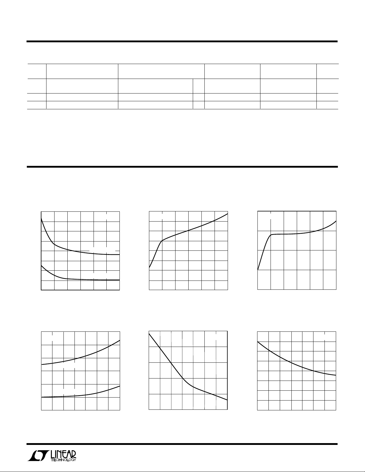
TEMPERATURE (°C)
–50
SAMPLING FREQUENCY (kHz)
4
5
6
25
LTC1250 G06
3
2
–25 0 50
1
0
8
7
75 100 150
VS = ±5V
TOTAL SUPPLY VOLTAGE, V+ TO V– (V)
4
2
SAMPLING FREQUENCY (kHz)
3
4
681012
LTC1250 G03
5
6
14
16
TA = 25°C
LECTRICAL C CHARA TERIST
E
ICS
VIN = 5V, TA = Operating Temperature Range, unless otherwise noted.
LTC1250M LTC1250C
SYMBOL PARAMETER CONDITIONS MIN TYP MAX MIN TYP MAX UNITS
Maximum Output Voltage Swing R
= 1k 4.0 4.3 4.0 4.3 V
L
RL = 100k 4.95 4.95 V
I
S
f
S
The ● denotes specifications which apply over the full operating
temperature range.
Note 1: These parametes are guaranteed by design. Thermocouple effects
preclude measurement of these voltage levels during automated testing.
Supply Current TA = 25°C 1.8 2.5 1.8 2.5 mA
Sampling Frequency TA = 25°C 3 3 kHz
filter at 0.1Hz. The LTC1250 is sample tested for noise; for 100% tested
parts contact LTC Marketing Dept.
Note 3: At T ≤ 0°C these parameters are guaranteed by design and not
tested.
Note 2: 0.1Hz to 10Hz noise is specified DC coupled in a 10s window;
0.1Hz to 1Hz noise is specified in a 100s window with an RC high-pass
UW
LPER
F
O
Input Noise vs Supply Voltage
1.6
1.4
1.2
)
P-P
1.0
0.8
0.6
INPUT NOISE (µV
0.4
0.2
0
681012
4
TOTAL SUPPLY VOLTAGE, V+ TO V– (V)
R
TA = 25°C
0.1Hz TO 10Hz
0.1Hz TO 1Hz
14
LTC1250 G01
ATYPICA
CCHARA TERIST
E
C
Supply Current vs Supply Voltage
4.0
TA = 25°C
3.5
3.0
2.5
2.0
1.5
SUPPLY CURRENT (mA)
1.0
0.5
0
16
4
TOTAL SUPPLY VOLTAGE, V+ TO V– (V)
681012
ICS
14
LTC1250 G02
Sampling Frequency vs Supply
Voltage
16
1.2
VS = ±5V
1.0
)
P-P
0.8
0.6
0.4
INPUT NOISE (µV
0.2
0
–50
–25 0
0.1Hz TO 10Hz
0.1Hz TO 1Hz
25 75
TEMPERATURE (°C)
50 100 125
LTC1250 G04
Supply Current vs TemperatureInput Noise vs Temperature
4.5
4.0
3.5
3.0
SUPPLY CURRENT (mA)
2.5
2.0
–50
–25
0
TEMPERATURE (°C)
Sampling Frequency vs
Temperature
VS = ±5V
50
25
75
100
LTC1250 G05
125
3
Page 4

LTC1250
TEMPERATURE (°C)
–25
10
100
1000
10075
LTC1250 G14
–50
125
BIAS CURRENT (
|
pA
|
)
50
025
VS = ±5V
FREQUENCY (Hz)
20
CMRR (dB)
40
80
120
140
1 100 1k 100k
LTC1250 G12
0
10 10k
60
100
VS = ±5V
V
CM
= 1V
RMS
LOAD RESISTANCE (kΩ)
0
0
OUTPUT SWING (V)
4
6
8
18
12
2
4
59
LTC1250 G09
2
14
16
10
13
6
7
8
V
S
= 16V
VS = 10V
VS = 5V
10
V– = GND
R
L
TO GND
LPER
Voltage Noise vs Frequency
80
VS = ±5V
70
= 10Ω
R
S
60
50
40
30
20
VOLTAGE NOISE (nV/√Hz)
10
0
1 100 1k 10k
10
F
O
FREQUENCY (Hz)
R
ATYPICA
LTC1250 G11
UW
CCHARA TERIST
E
C
Gain/Phase vs Frequency
100
80
60
40
GAIN (dB)
20
VS = ±5V OR
SINGLE 5V
0
= 25°C
T
A
= 100pF
C
L
–20
1k 100k 1M 10M
10k
GAIN
FREQUENCY (Hz)
ICS
PHASE:
R
L
= 100k
PHASE:
= 1k
R
L
LTC1250 G10
Bias Current (Magnitude) vs
Temperature
100
80
PHASE MARGIN (DEG)
60
40
20
0
–20
Overload Recovery
0.2
INPUT (V)
0
0
OUTPUT (V)
–5
500µs/DIV
A
= 100, RL = 100k, CL = 50pF, VS = ±5V
V
Transient Response
2V/DIV
4
A
V
1µs/DIV
= 1, RL = 100k, CL = 50pF, VS = ±5V
Common-Mode Input Range
vs Supply Voltage
8
TA = 25°C
6
4
2
0
–2
–4
INPUT COMMON MODE RANGE (V)
–6
–8
2
34
SUPPLY VOLTAGE (±V)
5
Output Swing vs Load
Resistance, Dual Supplies
10
9
VS = ±8V
8
7
6
VS = ±5V
5
4
VS = ±2.5V
3
OUTPUT SWING (±V)
2
1
0
1357
2
0
4
LOAD RESISTANCE (kΩ)
6
7
LTC1250 G07
R
TO GND
L
NEGATIVE SWING
POSITIVE SWING
6
8
9
LTC1250 G08
Common-Mode Rejection Ratio
vs Frequency
8
Output Voltage Swing vs Load
Resistance, Single Supply
10
Page 5

LPER
F
O
R
ATYPICA
UW
CCHARA TERIST
E
C
LTC1250
ICS
Output Swing vs Output Current,
±5V Supply
5
VS = ±5V
4
3
2
1
0
–1
–2
OUTPUT VOLTAGE (V)
–3
–4
–5
0.01
0.1 1 10
OUTPUT CURRENT (mA)
TEST CIRCUITS
Offset Test Circuit
100pF
100k
5V
–
LTC1250
+
–5V
7
6
OUTPUT
4
2
10Ω
3
1250 TC01
LTC1250 G16
10Ω
Output Swing vs Output Current,
Single 5V Supply
6
5
4
3
2
OUTPUT VOLTAGE (V)
1
0
0.01
100pF
100k
5V
–
LTC1250
+
7
4
–5V
2
3
VS = SINGLE 5V
0.1 1 10
OUTPUT CURRENT (mA)
6
800k
0.02µF
Short-Circuit Current
vs Temperature
40
VS = ±15V
30
20
10
0
–10
–20
SHORT-CIRCUIT CURRENT (mA)
–30
–40
LTC1250 G17
–25 0 50
–50
25
TEMPERATURE (°C)
DC to 10Hz Noise Test Circuit
(for DC to 1Hz Multiply All Capacitor Values by 10)
5V
–
1/2
LT1057
+
–5V
8
1
800k 800k
4
0.04µF
0.01µF
2
3
6
–
1/2
LT1057
5
+
–
V
= V
OUT
+
V
= V
OUT
75 100 125
7
LTC1250 G18
OUTPUT
1250 TC02
PPLICATI
A
U
O
S
I FOR ATIO
WU
U
Input Noise
The LTC1250, like all CMOS amplifiers, exhibits two types
of low frequency noise: thermal noise and 1/f noise. The
LTC1250 uses several design modifications to minimize
these noise sources. Thermal noise is minimized by raising the gM of the front-end transistors by running them at
high bias levels and using large transistor geometries. 1/f
noise is combated by optimizing the zero-drift nulling loop
to run at twice the 1/f corner frequency, allowing it to
reduce the inherently high CMOS 1/f noise to near thermal
levels at low frequencies. The resultant noise spectrum is
quite low at frequencies below the internal 5kHz clock
80
70
60
50
40
30
20
VOLTAGE NOISE (nV/√Hz)
10
0
0.01 1
OP-27
LTC1250
OP-07
0.1
FREQUENCY (Hz)
VS = ±5V
= 10Ω
R
S
LTC1250 F01
Figure 1. Voltage Noise vs Frequency
5
Page 6

LTC1250
PPLICATI
A
U
O
S
I FOR ATIO
WU
U
frequency, approaching the best bipolar op amps at 10Hz
and surpassing them below 1Hz (Figure 1). All this is
accomplished in an industry-standard pinout; the LTC1250
requires no external capacitors, no nulling or clock signals, and conforms to industry-standard 8-pin DIP and 8pin SOIC packages.
Input Capacitance and Compensation
The large input transistors create a parasitic 55pF capacitance from each input to V+. This input capacitance will
react with the external feedback resistors to form a pole
which can affect amplifier stability. In low gain, high
impedance configurations, the pole can land below the
unity-gain frequency of the feedback network and degrade
phase margin, causing ringing, oscillation, and other
unpleasantness. This is true of any op amp, however, the
55pF capacitance at the LTC1250’s inputs can affect
stability with a feedback network impedance as low as
1.9k. This effect can be eliminated by adding a capacitor
across the feedback resistor, adding a zero which cancels
the input pole (Figure 2). The value of this capacitor should
be:
C
F
pF
55
≥
A
V
where AV = closed-loop gain. Note that CF is not dependent
on the value of RF. Circuits with higher gain (AV > 50) or
low loop impedance should not require CF for stability.
C
F
R
F
R
IN
C
P
Figure 2. CF Cancels Phase Shift Due to Parasitic C
–
LTC1250
+
1250 F02
P
Larger values of CF, commonly used in band-limited DC
circuits, may actually increase low frequency noise. The
nulling circuitry in the LTC1250 closes a loop that includes
the external feedback network during part of its cycle. This
loop must settle to its final value within 150µ s or it will not
fully cancel the 1/f noise spectrum and the low frequency
noise of the part will rise. If the loop is underdamped (large
RF, no CF) it will ring for more than 150µs and the noise
and offset will suffer.
The solution is to add CF as above but beware! Too large
a value of CF will overdamp the loop, again preventing it
from reaching a final value by the 150µs deadline. This
condition doesn’t affect the LTC1250’s offset or output
stability, but 1/f noise begins to rise. As a rule of thumb,
the RFCF feedback pole should be ≥ 7kHz (1/150µs, the
frequency at which the loop settles) for best 1/f performance; values between 100pF and 500pF work well with
feedback resistors below 100k. This ensures adequate
gain at 7kHz for the LTC1250 to properly null. High value
feedback resistors (above 1M) may require experimentation to find the correct value because parasitics, both in
the LTC1250 and on the PC board, play an increasing role.
Low value resistors (below 5k) may not require a capacitor at all.
Input Bias Current
The inputs of the LTC1250, like all zero-drift op amps,
draw only small switching spikes of AC bias current; DC
leakage current is negligible except at very high temperatures. The large front-end transistors cause switching
spikes 3 to 4 times greater than standard zero-drift op
amps: the ±50pA bias current spec is still many times
better than most bipolar parts. The spikes don’t match
from one input pin to the other, and are sometimes (but
not always) of opposite polarity. As a result, matching the
impedances at the inputs (Figure 3) will not cancel the bias
current, and may cause additional errors. Don’t do it.
R
F
R
IN
Figure 3. Extra Resistor Will
–
LTC1250
+
Not
Cancel Bias Current Errors
1250 F03
6
Page 7

LTC1250
–
+
LTC1250
47k
R
F
C
F
0.01
1250 F04
U
O
PPLICATI
A
Output Drive
The LTC1250 includes an enhanced output stage which
provides nearly symmetrical output source/sink currents.
This output is capable of swinging a minimum of ±4V into a
1k load with ±5V supplies, and can sink or source >20mA
into low impedance loads. Lightly loaded (RL ≥100k), the
LTC1250 will swing to within millivolts of either rail. In single
supply applications, it will typically swing 4.3V into a 1k load
with a 5V supply.
Minimizing External Errors
The input noise, offset voltage, and bias current specs for the
LTC1250 are all well below the levels of circuit board
parasitics. Thermocouples between the copper pins of the
LTC1250 and the tin/lead solder used to connect them can
overwhelm the offset voltage of the LTC1250, especially if a
soldering iron has been around recently. Note also that when
the LTC1250’s output is heavily loaded, the chip may
dissipate substantial power, raising the temperature of the
package and aggravating thermocouples at the inputs.
Although the LTC1250 will maintain its specified accuracy
under these conditions, care must be taken in the layout to
prevent or compensate circuit errors. Be especially careful
of air currents when measuring low frequency noise; nearby
moving objects (like people) can create very large noise
peaks with an unshielded circuit board. For more detailed
explanations and advice on how to avoid these errors, see
the LTC1051/LTC1053 data sheet.
S
I FOR ATIO
WU
U
the previous page). Applications which require spike-free
output in addition to minimum noise will need a low-pass
filter after the LTC1250; a simple RC will usually do the job
(Figure 4). The LTC1051/LTC1053 data sheet includes more
information about zero-drift amplifier sampling behavior.
Figure 4. RC Output Pole Limits Bandwidth to 330Hz
Single Supply Operation
The LTC1250 will operate with single supply voltages as low
as 4.5V, and the output swings to within millivolts of either
supply when lightly loaded. The input stage will common
mode to within 250mV of ground with a single 5V supply,
and will common mode to ground with single supplies
above 11V. Most bridge transducers bias their inputs above
ground when powered from single supplies, allowing them
to interface directly to the LTC1250 in single supply applications. Single-ended, ground-referenced signals will need to
be level shifted slightly to interface to the LTC1250’s inputs.
Fault Conditions
Sampling Behavior
The LTC1250’s zero-drift nulling loop samples the input at
≈ 5kHz, allowing it to process signals below 2kHz with no
aliasing. Signals above this frequency may show aliasing
behavior, although wideband internal circuitry generally
keeps errors to a minimum. The output of the LTC1250 will
have small spikes at the clock frequency and its harmonics;
these will vary in amplitude with different feedback configurations. Low frequency or band-limited systems should not
be affected, but systems with higher bandwidth
Information furnished by Linear Technology Corporation is believed to be accurate and reliable.
However, no responsibility is assumed for its use. Linear Technology Corporation makes no representation that the interconnection of its circuits as described herein will not infringe on existing patent rights.
(oversampling A/Ds, for example) may need to filter out
these clock artifacts. Output spikes can be minimized with a
large feedback capacitor, but this will adversely affect noise
performance (see Input Capacitance and Compensation on
The LTC1250 is designed to withstand most external fault
conditions without latch-up or damage. However, unusually
severe fault conditions can destroy the part. All pins are
protected against faults of ±25mA or 5V beyond either
supply, whichever comes first. If the external circuitry can
exceed these limits, series resistors or voltage clamp diodes
should be included to prevent damage.
The LTC1250 includes internal protection against ESD damage. All data sheet parameters are maintained to 1kV ESD on
any pin; beyond 1kV, the input bias and offset currents will
increase, but the remaining specs are unaffected and the
part remains functional to 5kV at the input pins and 8kV at the
output pin. Extreme ESD conditions should be guarded
against by using standard anti-static precautions.
7
Page 8

LTC1250
PPLICATITYPICAL
Reference Buffer
O
U
SA
Differential Thermocouple Ampliifer
15V
7.5k
7
3
2
+
LTC1250
–
4
31
LM399
4
2
±10ppm ERROR AT ±15mA
OUTPUT NOISE
1µV
P-P
2.5µV/°C DRIFT (DUE TO LM399)
PACKAGE DESCRIPTIO
J8 Package 8-Lead Ceramic DIP N8 Package 8-Lead Plastic DIP
CORNER LEADS OPTION
(4 PLCS)
0.023 – 0.045
(0.584 – 1.143)
HALF LEAD
0.045 – 0.068
(1.143 – 1.727)
FULL LEAD
OPTION
0.300 BSC
(0.762 BSC)
0.008 – 0.018
(0.203 – 0.457)
0.385 ± 0.025
(9.779 ± 0.635)
NOTE: LEAD DIMENSIONS APPLY TO SOLDER DIP/PLATE OR TIN PLATE LEADS.
OPTION
0° – 15°
0.005
(0.127)
MIN
0.025
(0.635)
RAD TYP
0.045 – 0.068
(1.143 – 1.727)
0.014 – 0.026
(0.360 – 0.660)
87
12
R1
6
–
†
TYPE K
V
CM
1250 TA03
10k
0.1%
+
R2
10k
0.1%
R4
1M
0.1%
5V
V
IN
V
OUT
LT1025
GND
–5V
U
Dimensions in inches (millimeters) unless otherwise noted.
0.405
(10.287)
MAX
65
0.255 ± 0.015*
(6.477 ± 0.381)
0.065
(1.651)
TYP
0.045 ± 0.015
(1.143 ± 0.381)
3
4
0.220 – 0.310
(5.588 – 7.874)
0.015 – 0.060
(0.381 – 1.524)
0.100 ± 0.010
(2.540 ± 0.254)
0.200
(5.080)
MAX
0.125
3.175
MIN
J8 0694
0.300 – 0.325
(7.620 – 8.255)
0.009 – 0.015
(0.229 – 0.381)
+0.025
0.325
–0.015
+0.635
8.255
()
–0.381
*THESE DIMENSIONS DO NOT INCLUDE MOLD FLASH OR PROTRUSIONS.
MOLD FLASH OR PROTURSIONS SHALL NOT EXCEED 0.010 INCH (0.254mm).
R3
C1
100pF
1M
0.1%
5V
7
2
3
–
LTC1250
+
6
4
–5V
C2
100pF
R5
3k
10mV/°C
†
R9
FOR BEST ACCURACY, THERMOCOUPLE
33k
RESISTANCE SHOULD BE LESS THAN 100Ω
0.400*
(10.160)
MAX
(1.143 – 1.651)
0.100 ± 0.010
(2.540 ± 0.254)
876
1234
0.045 – 0.065
5
0.018 ± 0.003
(0.457 ± 0.076)
V
OUT
100mV/°C
R6
7.5k
1%
R7
500Ω
FULL-SCALE TRIM
R8
5k
1%
1250 TA04
0.130 ± 0.005
(3.302 ± 0.127)
0.125
0.015
(3.175)
MIN
(0.380)
MIN
N8 0694
8
S8 Package 8-Lead Plastic SOIC
0.010 – 0.020
(0.254 – 0.508)
0.008 – 0.010
(0.203 – 0.254)
*THESE DIMENSIONS DO NOT INCLUDE MOLD FLASH OR PROTRUSIONS.
MOLD FLASH OR PROTRUSIONS SHALL NOT EXCEED 0.006 INCH (0.15mm).
× 45°
0.016 – 0.050
0.406 – 1.270
0°– 8° TYP
0.053 – 0.069
(1.346 – 1.752)
0.014 – 0.019
(0.355 – 0.483)
Linear Technology Corporation
1630 McCarthy Blvd., Milpitas, CA 95035-7487
(408) 432-1900
●
FAX
: (408) 434-0507
●
TELEX
: 499-3977
0.050
(1.270)
BSC
0.004 – 0.010
(0.101 – 0.254)
0.228 – 0.244
(5.791 – 6.197)
0.189 – 0.197*
(4.801 – 5.004)
8
1
7
2
5
6
0.150 – 0.157*
(3.810 – 3.988)
3
LINEAR TECHNOLOGY CORPORATION 1994
SO8 0294
4
LT/GP 0894 2K REV A • PRINTED IN USA
 Loading...