

Datasheet LTC1199LIS8, LTC1199LCMS8, LTC1199IS8, LTC1199IMS8, LTC1199CS8 Datasheet (Linear Technology)
...Page 1
1
LTC1197/LTC1197L
LTC1199/LTC1199L
10-Bit, 500ksps ADCs in
MSOP with Auto Shutdown
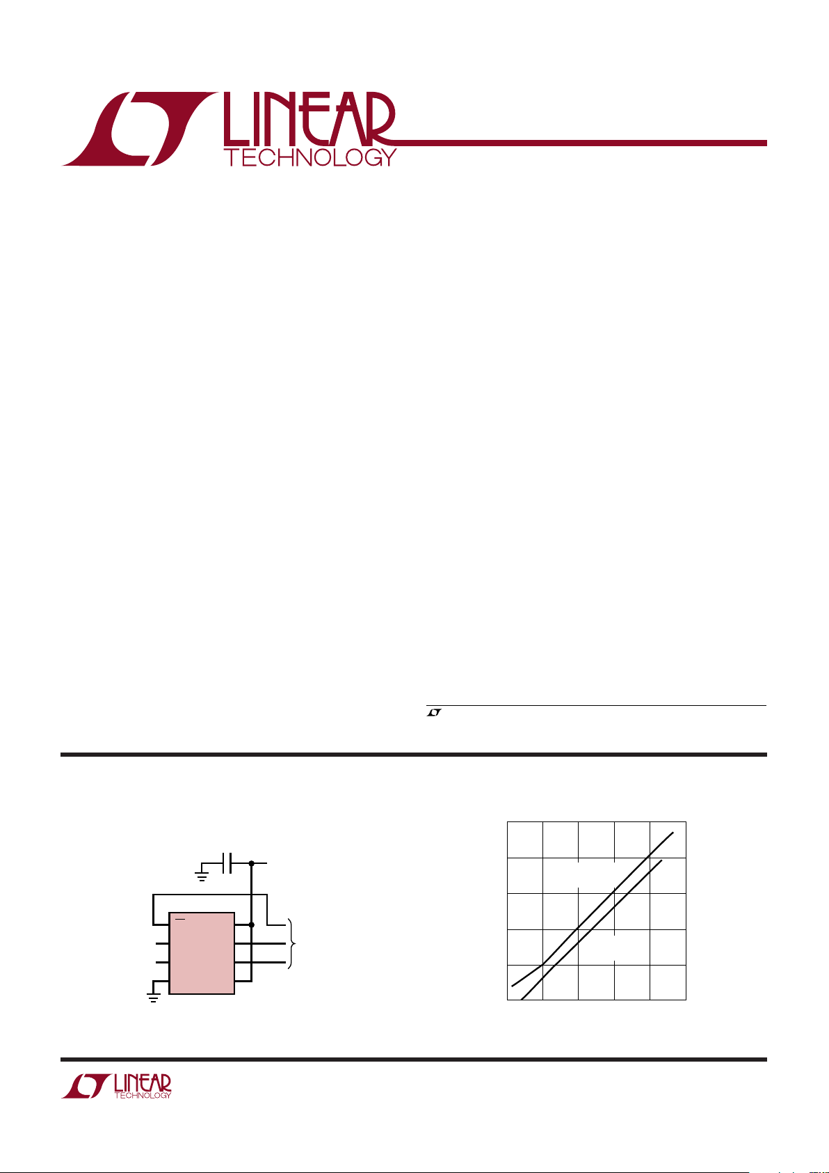
Single 2.7V Supply, 250ksps, 10-Bit Sampling ADC
Supply Current vs Sampling Frequency
SAMPLING FREQUENCY (kHz)
0.01
SUPPLY CURRENT (µA)
100
1000
10000
100
1197/99 G03
10
1
0.1
0.1
1
10
1000
VCC = 5V
f
CLK
= 7.2MHz
VCC = 2.7V
f
CLK
= 3.5MHz
1
2
3
4
8
7
6
5
CS
+IN
–IN
GND
V
CC
CLK
D
OUT
V
REF
LTC1197L
1197/99 TA01
ANALOG INPUT
0V TO 2.7V RANGE
2.7V
1µF
SERIAL DATA LINK TO
ASIC, PLD, MPU, DSP
OR SHIFT REGISTERS
The LTC®1197/LTC1197L/LTC1199/LTC1199L are
10-bit A/D converters with sampling rates up to 500kHz.
They have 2.7V (L) and 5V versions and are offered in
8-pin MSOP and SO packages. Power dissipation is typically only 2.2mW at 2.7V (25mW at 5V) during full speed
operation. The automatic power down reduces supply
current linearly as sample rate is reduced. These 10-bit,
switched-capacitor, successive approximation ADCs include a sample-and-hold. The LTC1197/LTC1197L have a
differential analog input with an adjustable reference pin.
The LTC1199/LTC1199L offer a software-selectable
2-channel MUX.
The 3-wire serial I/O, MSOP and SO-8 packages, 2.7V
operation and extremely high sample rate-to-power ratio
make these ADCs ideal choices for compact, low power
high speed systems.
These circuits can be used in ratiometric applications or
with external references. The high impedance analog
inputs and the ability to operate with reduced spans below
1V full scale (LTC1197/LTC1197L) allow direct connection to signal sources in many applications, eliminating
the need for gain stages.
■
8-Pin MSOP and SO Packages
■
10-Bit Resolution at 500ksps
■
Single Supply: 5V or 3V
■
Low Power at Full Speed:
25mW Typ at 5V
2.2mW Typ at 2.7V
■
Auto Shutdown Reduces Power Linearly
at Lower Sample Rates
■
10-Bit Upgrade to 8-Bit LTC1196/LTC1198
■
SPI and MICROWIRETM Compatible Serial I/O
■
Low Cost
, LTC and LT are registered trademarks of Linear Technology Corporation.
MICROWIRE is a trademark of National Semiconductor Corporation.
■
High Speed Data Acquisition
■
Portable or Compact Instrumentation
■
Low Power or Battery-Operated Instrumentation
FEATURES
DESCRIPTIO
U
APPLICATIO S
U
TYPICAL APPLICATIO
U
Page 2
2
LTC1197/LTC1197L
LTC1199/LTC1199L
Operating Temperature Range
LTC1197C/LTC1197LC
LTC1199C/LTC1199LC........................... 0°C to 70°C
LTC1197I/LTC1197LI
LTC1199I/LTC1199LI ........................ –45°C to 85°C
Lead Temperature (Soldering, 10 sec)................. 300°C
Supply Voltage (VCC) ............................................... 12V
Voltage
Analog Input ..................... GND – 0.3V to V
CC
+ 0.3V
Digital Input ................................ GND – 0.3V to 12V
Digital Output .................... GND – 0.3V to V
CC
+ 0.3V
Power Dissipation.............................................. 500mW
Storage Temperature Range .................– 65°C to 150°C
(Notes 1, 2)
LTC1197 LTC1199
SYMBOL PARAMETER CONDITIONS MIN TYP MAX MIN TYP MAX UNITS
V
CC
Supply Voltage 4 9 4 6 V
VCC = 5V Operation
f
CLK
Clock Frequency ● 0.05 7.2 0.05 7.2 MHz
t
CYC
Total Cycle Time 14 16 CLK
t
SMPL
Analog Input Sampling Time 1.5 1.5 CLK
t
hCS
Hold Time CS Low After Last CLK↑ 13 13 ns
ORDER PART
NUMBER
MS8 PART MARKING S8 PART MARKING
1197L
1197LI
1197
1197I
LTC1197CS8
LTC1197IS8
LTC1197LCS8
LTC1197LIS8
ORDER PART
NUMBER
LTC1197CMS8
LTC1197IMS8
LTC1197LCMS8
LTC1197LIMS8
LTBL
LTJA
T
JMAX
= 150°C, θJA = 175°C/W
1
2
3
4
8
7
6
5
TOP VIEW
S8 PACKAGE
8-LEAD PLASTIC SO
CS
+IN
–IN
GND
V
CC
CLK
D
OUT
V
REF
ORDER PART
NUMBER
MS8 PART MARKING S8 PART MARKING
1199L
1199LI
1199
1199I
LTC1199CS8
LTC1199IS8
LTC1199LCS8
LTC1199LIS8
ORDER PART
NUMBER
LTC1199CMS8
LTC1199IMS8
LTC1199LCMS8
LTC1199LIMS8
LTCM
LTWC
T
JMAX
= 150°C, θJA = 210°C/W
1
2
3
4
CS
+IN
–IN
GND
8
7
6
5
V
CC
CLK
D
OUT
V
REF
TOP VIEW
MS8 PACKAGE
8-LEAD PLASTIC MSOP
1
2
3
4
CS
CH0
CH1
GND
8
7
6
5
V
CC
CLK
D
OUT
D
IN
TOP VIEW
MS8 PACKAGE
8-LEAD PLASTIC MSOP
T
JMAX
= 150°C, θJA = 210°C/W
T
JMAX
= 150°C, θJA = 175°C/W
1
2
3
4
8
7
6
5
TOP VIEW
S8 PACKAGE
8-LEAD PLASTIC SO
CS
CH0
CH1
GND
V
CC
CLK
D
OUT
D
IN
ABSOLUTE AXI U RATI GS
WWWU
PACKAGE/ORDER I FOR ATIO
UU
W
LTKV
LTKW
LTFL
LTWB
Consult factory for parts specified with wider operating temperature ranges.
RECO E DED OPERATI G CO DITIO S
UUUUWW
The ● denotes the specifications which apply over
the full operating temperature range, otherwise specifications are at TA = 25°C.
Page 3
3
LTC1197/LTC1197L
LTC1199/LTC1199L
LTC1197 LTC1199
SYMBOL PARAMETER CONDITIONS MIN TYP MAX MIN TYP MAX UNITS
VCC = 5V Operation
t
suCS
Setup Time CS↓ Before First CLK↑ 26 26 ns
(See Figures 1, 2)
t
hDI
Hold Time DIN After CLK↑ LTC1199 26 ns
t
suDI
Setup Time DIN Stable Before CLK↑ LTC1199 26 ns
t
WHCLK
CLK High Time f
CLK
= f
CLK(MAX)
40% 40% 1/f
CLK
t
WLCLK
CLK Low Time f
CLK
= f
CLK(MAX)
40% 40% 1/f
CLK
t
WHCS
CS High Time Between Data Transfer Cycles 32 32 ns
t
WLCS
CS Low Time During Data Transfer 13 15 CLK
The ● denotes the specifications which apply over the full operating temperature range, otherwise specifications are at TA = 25°C.
VCC = 5V, V
REF
= 5V, f
CLK
= f
CLK(MAX)
as defined in Recommended Operating Conditions, unless otherwise noted.
–0.05V to VCC + 0.05V
LTC1197 LTC1199
PARAMETER CONDITIONS MIN TYP MAX MIN TYP MAX UNITS
Offset Error ● ±2 ±2 LSB
Linearity Error (Note 3) ● ±1 ±1 LSB
Gain Error ● ±4 ±4 LSB
No Missing Codes Resolution ● 10 10 Bits
Analog Input Range V
Reference Input Range LTC1197, VCC ≤ 6V 0.2 VCC + 0.05V V
LTC1197, V
CC
> 6V 0.2 6 V
Analog Input Leakage Current (Note 4) ● ±1 ±1 µA
LTC1197L LTC1199L
SYMBOL PARAMETER CONDITIONS MIN TYP MAX MIN TYP MAX UNITS
V
CC
Supply Voltage 2.7 4 2.7 4 V
VCC = 2.7V Operation
f
CLK
Clock Frequency ● 0.01 3.5 0.01 3.5 MHz
t
CYC
Total Cycle Time 14 16 CLK
t
SMPL
Analog Input Sampling Time 1.5 1.5 CLK
t
hCS
Hold Time CS Low After Last CLK↑ 40 40 ns
t
suCS
Setup Time CS↓ Before First CLK↑ 78 78 ns
(See Figures 1, 2)
t
hDI
Hold Time DIN After CLK↑ LTC1199L 78 ns
t
suDI
Setup Time DIN Stable Before CLK↑ LTC1199L 78 ns
t
WHCLK
CLK High Time f
CLK
= f
CLK(MAX)
40% 40% 1/f
CLK
t
WLCLK
CLK Low Time f
CLK
= f
CLK(MAX)
40% 40% 1/f
CLK
t
WHCS
CS High Time Between Data Transfer Cycles 96 96 ns
t
WLCS
CS Low Time During Data Transfer 13 15 CLK
The ● denotes the specifications which apply over
the full operating temperature range, otherwise specifications are at TA = 25°C.
RECO E DED OPERATI G CO DITIO S
UUUUWW
CO VERTER A D ULTIPLEXER CHARACTERISTICS
U
W
U
Page 4
4
LTC1197/LTC1197L
LTC1199/LTC1199L
The ● denotes the specifications which apply over the full operating temperature range, otherwise specifications are at TA = 25°C.
VCC = 2.7V, V
REF
= 2.5V (LTC1197L), f
CLK
= f
CLK(MAX)
as defined in Recommended Operating Conditions, unless otherwise noted.
–0.05V to VCC + 0.05V
DYNAMIC ACCURACY
UW
VCC = 5V, V
REF
= 5V, f
CLK
= f
CLK(MAX)
as defined in Recommended Operating Conditions, unless otherwise noted.
LTC1197 LTC1199
SYMBOL PARAMETER CONDITIONS MIN TYP MAX MIN TYP MAX UNITS
S/(N + D) Signal-to-Noise Plus 100kHz Input Signal 60 60 dB
Distortion Ratio
THD Total Harmonic Distortion 100kHz Input Signal –64 –64 dB
First 5 Harmonics
Peak Harmonic or Spurious Noise 100kHz Input Signal –68 –68 dB
IMD Intermodulation Distortion f
IN1
= 97.046kHz, f
IN2
= 102.905kHz
2nd Order Terms –65 –65 dB
3rd Order Terms –70 –70 dB
VCC = 2.7V, V
REF
= 2.5V, f
CLK
= f
CLK(MAX)
as defined in Recommended Operating Conditions, unless otherwise noted.
LTC1197L LTC1199L
SYMBOL PARAMETER CONDITIONS MIN TYP MAX MIN TYP MAX UNITS
S/(N + D) Signal-to-Noise Plus 50kHz Input Signal 58 58 dB
Distortion Ratio
THD Total Harmonic Distortion 50kHz Input Signal –60 –60 dB
First 5 Harmonics
Peak Harmonic or Spurious Noise 50kHz Input Signal – 63 –63 dB
IMD Intermodulation Distortion f
IN1
= 48.5kHz, f
IN2
= 51.5kHz
2nd Order Terms –60 –60 dB
3rd Order Terms –65 –65 dB
LTC1197L LTC1199L
PARAMETER CONDITIONS MIN TYP MAX MIN TYP MAX UNITS
Offset Error ● ±2 ±2 LSB
Linearity Error (Note 3) ● ±1 ±1 LSB
Gain Error ● ±4 ±4 LSB
No Missing Codes Resolution ● 10 10 Bits
Analog Input Range V
Reference Input Range LTC1197L 0.2 VCC + 0.05V V
Analog Input Leakage Current (Note 4) ● ±1 ±1 µA
CO VERTER A D ULTIPLEXER CHARACTERISTICS
U
W
U
Page 5
5
LTC1197/LTC1197L
LTC1199/LTC1199L
LTC1197 LTC1199
SYMBOL PARAMETER CONDITIONS MIN TYP MAX MIN TYP MAX UNITS
V
IH
High Level Input Voltage VCC = 5.25V ● 2.4 2.4 V
V
IL
Low Level Input Voltage VCC = 4.75V ● 0.8 0.8 V
I
IH
High Level Input Current VIN = V
CC
● 2.5 2.5 µA
I
IL
Low Level Input Current VIN = 0V ● –2.5 –2.5 µA
V
OH
High Level Output Voltage VCC = 4.75V, IO = 10µA ● 4.5 4.74 4.5 4.74 V
VCC = 4.75V, IO = 360µA ● 2.4 4.72 2.4 4.72 V
V
OL
Low Level Output Voltage VCC = 4.75V, IO = 1.6mA ● 0.4 0.4 V
I
OZ
Hi-Z Output Leakage CS = High ● ±3 ±3 µA
I
SOURCE
Output Source Current V
OUT
= 0V –25 –25 mA
I
SINK
Output Sink Current V
OUT
= V
CC
45 45 mA
I
REF
Reference Current (LTC1197) CS = V
CC
● 0.001 3 µA
f
SMPL
= f
SMPL(MAX)
● 0.5 1 mA
I
CC
Supply Current CS = V
CC
● 0.001 3 0.001 3 µA
f
SMPL
= f
SMPL(MAX)
● 4.5 8 5 8.5 mA
P
D
Power Dissipation f
SMPL
= f
SMPL(MAX)
22.5 25 mW
The ● denotes the specifications which apply
over the full operating temperature range, otherwise specifications are at TA = 25°C. VCC = 5V, V
REF
= 5V, unless otherwise noted.
DIGITAL AND DC ELECTRICAL CHARACTERISTICS
U
The ● denotes the specifications which apply over the full operating temperature range, otherwise specifications are at TA = 25°C.
VCC = 2.7V, V
REF
= 2.5V, unless otherwise noted.
LTC1197L LTC1199L
SYMBOL PARAMETER CONDITIONS MIN TYP MAX MIN TYP MAX UNITS
V
IH
High Level Input Voltage VCC = 3.6V ● 1.9 1.9 V
V
IL
Low Level Input Voltage VCC = 2.7V ● 0.45 0.45 V
I
IH
High Level Input Current VIN = V
CC
● 2.5 2.5 µA
I
IL
Low Level Input Current VIN = 0V ● –2.5 –2.5 µA
V
OH
High Level Output Voltage VCC = 2.7V, IO = 10µA ● 2.3 2.60 2.3 2.60 V
V
CC
= 2.7V, IO = 360µA ● 2.1 2.45 2.1 2.45 V
V
OL
Low Level Output Voltage VCC = 2.7V, IO = 400µA ● 0.3 0.3 V
I
OZ
Hi-Z Output Leakage CS = High ● ±3 ±3 µA
I
SOURCE
Output Source Current V
OUT
= 0V – 6.5 –6.5 mA
I
SINK
Output Sink Current V
OUT
= V
CC
11 11 mA
I
REF
Reference Current (LTC1197L) CS = V
CC
● 0.001 3.0 µA
f
SMPL
= f
SMPL(MAX)
● 0.250 0.5 mA
I
CC
Supply Current CS = V
CC
● 0.001 3 0.001 3 µA
f
SMPL
= f
SMPL(MAX)
● 0.8 2 0.8 2 mA
P
D
Power Dissipation f
SMPL
= f
SMPL(MAX)
2.2 2.2 mW
Page 6

6
LTC1197/LTC1197L
LTC1199/LTC1199L
AC CHARACTERISTICS
The ● denotes the specifications which apply over the full operating temperature range, otherwise specifications are at TA = 25°C.
VCC = 5V, V
REF
= 5V, f
CLK
= f
CLK(MAX)
as defined in Recommended Operating Conditions, unless otherwise noted.
LTC1197 LTC1199
SYMBOL PARAMETER CONDITIONS MIN TYP MAX MIN TYP MAX UNITS
t
CONV
Conversion Time (See Figures 1, 2) ● 1.4 1.4 µs
f
SMPL(MAX)
Maximum Sampling Frequency ● 500 450 kHz
t
dDO
Delay Time, CLK↑ to D
OUT
Data Valid C
LOAD
= 20pF 68 78 68 78 ns
● 100 100 ns
t
dis
Delay Time, CS↑ to D
OUT
Hi-Z ● 75 150 75 150 ns
t
en
Delay Time, CLK↓ to D
OUT
Enabled C
LOAD
= 20pF ● 40 68 40 68 ns
t
hDO
Time Output Data Remains C
LOAD
= 20pF ● 15 55 15 55 ns
Valid After CLK↑
t
r
D
OUT
Rise Time C
LOAD
= 20pF ● 10 20 10 20 ns
t
f
D
OUT
Fall Time C
LOAD
= 20pF ● 10 20 10 20 ns
C
IN
Input Capacitance Analog Input On Channel 20 20 pF
Analog Input Off Channel 5 5 pF
Digital Input 5 5 pF
LTC1197L LTC1199L
SYMBOL PARAMETER CONDITIONS MIN TYP MAX MIN TYP MAX UNITS
t
CONV
Conversion Time (See Figures 1, 2) ● 2.9 2.9 µs
f
SMPL(MAX)
Maximum Sampling Frequency ● 250 210 kHz
t
dDO
Delay Time, CLK↑ to D
OUT
Data Valid C
LOAD
= 20pF 130 180 130 180 ns
● 250 250 ns
t
dis
Delay Time, CS↑ to D
OUT
Hi-Z ● 120 250 120 250 ns
t
en
Delay Time, CLK↓ to D
OUT
Enabled C
LOAD
= 20pF ● 100 200 100 200 ns
t
hDO
Time Output Data Remains C
LOAD
= 20pF ● 30 120 30 120 ns
Valid After CLK↑
t
r
D
OUT
Rise Time C
LOAD
= 20pF ● 15 40 15 40 ns
t
f
D
OUT
Fall Time C
LOAD
= 20pF ● 15 40 15 40 ns
C
IN
Input Capacitance Analog Input On Channel 20 20 pF
Analog Input Off Channel 5 5 pF
Digital Input 5 5 pF
The ● denotes the specifications which apply over the full operating temperature range, otherwise specifications are at TA = 25°C.
VCC = 2.7V, V
REF
= 2.5V, f
CLK
= f
CLK(MAX)
as defined in Recommended Operating Conditions, unless otherwise noted.
Note 1: Absolute Maximum Ratings are those values beyond which the life
of a device may be impaired.
Note 2: All voltage values are with respect to GND.
Note 3: Integral nonlinearity is defined as deviation of a code from a
straight line passing through the actual endpoints of the transfer curve.
The deviation is measured from the center of the quantization band.
Note 4: Channel leakage current is measured after the channel selection.
Page 7
7
LTC1197/LTC1197L
LTC1199/LTC1199L
Supply Current
vs Sampling Frequency
Supply Current vs Clock Rate*
FREQUENCY (kHz)
10
8
SUPPLY CURRENT (mA)
10
12
14
16
100 1000 10000
1197/99 G01
6
4
2
0
18
20
VCC = 9V
VCC = 5V
VCC = 2.7V
SAMPLING FREQUENCY (kHz)
0.01
SUPPLY CURRENT (µA)
100
1000
10000
100
1197/99 G03
10
1
0.1
0.1
1
10
1000
VCC = 5V
f
CLK
= 7.2MHz
VCC = 2.7V
f
CLK
= 3.5MHz
Supply Current vs Supply Voltage
SUPPLY VOLTAGE (V)
10
SUPPLY CURRENT (mA)
SHUTDOWN CURRENT (nA)
8
10
12
56789
1197/99 G02
6
4
0
2
3
4
2
16
14
40
50
60
30
20
0
10
80
70
SHUTDOWN
MODE
ACTIVE
MODE
f
CLK
= 3.5MHz
T
A
= 25°C
CODE
0
–1.0
INL (LSBs)
–0.5
0
0.5
1.0
128 256 384 512
1197/99 G04
640 768 896 1024
VCC = V
REF
= 5V
f
CLK
= 7.2MHz
T
A
= 25°C
INL Plot
FREQUENCY (kHz)
0
AMPLITUDE (dB)
–40
–20
–30
–10
0
1197/99 G06
–60
–80
–50
–70
–90
–100
50
100 150 200 250
f
SMPL
= 500kHz
f
IN
= 97.045898kHz
LTC1197 4096 Point FFT
FREQUENCY (kHz)
1
4
ENOBs
5
6
7
8
10 100 1000
1197/99 G07
3
2
1
0
9
10
VCC = 2.7V
f
SMPL
= 250kHz
VCC = 5V
f
SMPL
= 500kHz
ENOBs vs Frequency Intermodulation Distortion Plot
*Part is continuously sampling, spending only a minimum amount of time in shutdown.
FREQUENCY (kHz)
0
AMPLITUDE (dB)
–20
–30
–40
–50
–60
–70
–80
–90
–100
–10
0
1197/99 G09
50
100 150 200 250
f
SMPL
= 500kHz
f
IN1
= 97.045898kHz
f
IN2
= 102.905273kHz
CODE
0
–1.0
DNL (LSBs)
–0.5
0
0.5
1.0
128 256 384 512
1197/99 G26
640 768 896 1024
VCC = V
REF
= 5V
f
CLK
= 7.2MHz
T
A
= 25°C
DNL Plot
THD vs Frequency
FREQUENCY (kHz)
10
THD (dB)
0
100 1000
1197/99 G08
–10
–20
–30
–40
–50
–60
–70
–80
TA = 25°C
V
CC
= 2.7V
f
SMPL
= 250kHz
VCC = 5V
f
SMPL
= 500kHz
TYPICAL PERFOR A CE CHARACTERISTICS
UW
Page 8
8
LTC1197/LTC1197L
LTC1199/LTC1199L
LTC1197L Change in Gain Error
vs Supply Voltage
LTC1197L Change in Offset
vs Supply Voltage
SUPPLY VOLTAGE (V)
0
CHANGE IN LINEARITY (LSBs)
0
0.6
1.0
4
1197/99 G10
–0.4
–0.8
0.4
0.2
0.8
–0.2
–0.6
–1.0
1
2
3
5
V
REF
= 2.5V
f
CLK
= 3.5MHz
LTC1197L Change in Linearity
vs Supply Voltage
SUPPLY VOLTAGE (V)
0
CHANGE IN OFFSET (LSBs)
–0.5
0
0.5
1.0
1.5
2.0
4
1197/99 G11
–1.0
–1.5
–2.0
1
2
3
5
V
REF
= 2.5V
f
CLK
= 3.5MHz
SUPPLY VOLTAGE (V)
0
CHANGE IN GAIN ERROR (LSBs)
0.2
0.6
1.0
4
1197/99 G12
–0.2
–0.6
0
0.4
0.8
–0.4
–0.8
–1.0
1
2
3
5
V
REF
= 2.5V
f
CLK
= 3.5MHz
LTC1197 Offset Error
vs Reference Voltage
LTC1197 Gain Error
vs Reference Voltage
LTC1197 Change in Linearity
vs Supply Voltage
SUPPLY VOLTAGE (V)
0
–1.0
CHANGE IN LINEARITY (LSBs)
–0.8
–0.4
–0.2
0
1.0
0.4
2
4
59
1197/99 G13
–0.6
0.6
0.8
0.2
13
6
7
8
V
REF
= 4V
f
CLK
= 7MHz
T
A
= 25°C
LTC1197 Change in Offset
vs Supply Voltage
SUPPLY VOLTAGE (V)
0
–2.0
CHANGE IN OFFSET (LSBs)
1.5
2.0
1.0
0.5
0
–0.5
–1.0
–1.5
1197/99 G14
123456789
V
REF
= 4V
f
CLK
= 7MHz
T
A
= 25°C
LTC1197 Change in Gain Error
vs Supply Voltage
SUPPLY VOLTAGE (V)
0
CHANGE IN GAIN ERROR (LSBs)
–2.0
1.0
0.5
0
1.5
2.0
2
4
59
1197/99 G15
–1.5
–1.0
–0.5
13
6
7
8
V
REF
= 4V
f
CLK
= 7MHz
T
A
= 25°C
LTC1197 Linearity Error
vs Reference Voltage
REFERENCE VOLTAGE (V)
0
LINEARITY ERROR (LSBs)
1.0
1.5
4
1197/99 F16
0.5
0
1
2
3
5
2.0
VCC = 5V
f
CLK
= 7.2MHz
T
A
= 25°C
REFERENCE VOLTAGE (V)
0
OFFSET ERROR (LSBs)
1.5
2.0
2.5
4
1197/99 G17
1.0
0.5
0
1
2
3
5
VCC = 5V
f
CLK
= 7.2MHz
T
A
= 25°C
REFERENCE VOLTAGE (V)
0
GAIN ERROR (LSBs)
1.0
1.5
4
1197/99 F18
0.5
0
1
2
3
5
2.0
VCC = 5V
f
CLK
= 7.2MHz
T
A
= 25°C
TYPICAL PERFOR A CE CHARACTERISTICS
UW
Page 9
9
LTC1197/LTC1197L
LTC1199/LTC1199L
Linearity vs Temperature
TEMPERATURE (°C)
–55 –30
0
LINEARITY ERROR (LSBs)
0.2
0.5
–5 45 70
1197/99 G19
0.1
0.4
0.3
20 95 120
VCC = 5V
V
REF
= 5V
f
CLK
= 7.2MHz
Gain Error vs Temperature
TEMPERATURE (°C)
–55 –30
–1.0
–1.2
–1.4
GAIN ERROR (LSBs)
0
–5 45 70
1197/99 G21
–0.2
–0.4
–0.6
–0.8
20 95 120
VCC = 5V
V
REF
= 5V
f
CLK
= 7.2MHz
Offset vs Temperature
TEMPERATURE (°C)
–55 –30
–1.0
OFFSET VOLTAGE (LSBs)
0
–5 45 70
1197/99 G20
–0.2
–0.3
–0.4
–0.5
–0.6
–0.7
–0.8
–0.9
–0.1
20 95 120
VCC = 5V
V
REF
= 5V
f
CLK
= 7.2MHz
*As the CLK frequency is decreased from 2MHz, minimum CLK frequency (∆error ≤ 0.1LSB)
represents the frequency at which a 0.1LSB shift in any code translation from its 2MHz value
is first detected.
†
Maximum CLK frequency represents the clock frequency at which a 0.1LSB shift in the error
at any code transition from its 3.5MHz value is first detected.
Acquisition Time
vs Source Resistance
Maximum Clock Frequency
vs Supply Voltage
Maximum Clock Frequency
†
vs Source Resistance
SOURCE RESISTANCE (Ω)
100 1000
0.1
ACQUISITION TIME (µs)
1
10
100
10000
1197/99 G25
VCC = V
REF
= 5V
T
A
= 25°C
+INPUT
R
SOURCE
+
V
IN
COM
SUPPLY VOLTAGE (V)
0
MAXIMUM CLOCK FREQUENCY (MHz)
6
8
10
11
8
1197/99 G26
4
2
5
7
9
3
1
0
2
4
6
19
3
5
7
10
V
REF
= 2.5V
T
A
= 25°C
SOURCE RESISTANCE (Ω)
100
100
MAXIMUM CLOCK FREQUENCY (kHz)
1000
10000
1000 10000
1197/99 G27
V
REF
= V
CC =
5V
T
A
= 25°C
+INPUT
R
SOURCE
–
V
IN
–INPUT
TEMPERATURE (°C)
–55
0.1
MINIMUM CLOCK FREQUENCY (kHz)
1
10
100
1000
–35 –15 5 25
1197/99 G22
45 65 85 105 125
V
REF
= 5V
V
CC
= 5V
Minimum Clock Frequency for
0.1LSB Error* vs Temperature
Digital Input Threshold
vs Supply Voltage
Input Channel Leakage Current
vs Temperature
SUPPLY VOLTAGE (V)
0
LOGIC THRESHOLD (V)
3
4
5
8
1197/99 G23
2
1
0
2
4
6
10
TA = 25°C
TEMPERATURE (°C)
0
LEAKAGE CURRENT (nA)
1
10
100
100
1197/99 G24
0.1
0.01
0.001
25
50
75
125
V
REF
= 5V
V
CC
= 5V
ON CHANNEL
OFF CHANNEL
TYPICAL PERFOR A CE CHARACTERISTICS
UW
Page 10

10
LTC1197/LTC1197L
LTC1199/LTC1199L
CS (Pin 1): Chip Select Input. A logic low on this input
enables the LTC1197/LTC1197L/LTC1199/LTC1199L.
Power shutdown is activated when CS is brought high.
+ IN, CH0 (Pin 2): Analog Input. This input must be free of
noise with respect to GND.
– IN, CH1 (Pin 3): Analog Input. This input must be free of
noise with respect to GND.
GND (Pin 4): Analog Ground. GND should be tied directly
to an analog ground plane.
V
REF
(Pin 5): LTC1197/LTC1197L Reference Input. The
reference input defines the span of the A/D converter and
must be kept free of noise with respect to GND.
DIN (Pin 5):
LTC1199/LTC1199L Digital Data Input. The
A/D configuration word is shifted into this input.
D
OUT
(Pin 6): Digital Data Output. The A/D conversion
result is shifted out of this output.
CLK (Pin 7): Shift Clock. This clock synchronizes the serial
data transfer.
VCC (Pin 8):
Positive Supply. This supply must be kept
free of noise and ripple by bypassing directly to the
analog ground plane. For LTC1199/LTC1199L, V
REF
is
tied internally to this pin.
–
+
C
SMPL
BIAS AND
SHUTDOWN CIRCUIT
SERIAL PORT
V
CC
CS CLK
D
OUT
+IN (CH0)
–IN (CH1)
MICROPOWER
COMPARATOR
CAPACITIVE DAC
SAR
V
REF
GND PIN NAMES IN PARENTHESES
REFER TO THE LTC1199/LTC1199L
(DIN)
UU
U
PI FU CTIO S
BLOCK DIAGRA
W
Page 11

11
LTC1197/LTC1197L
LTC1199/LTC1199L
Load Circuit for t
dDO
, tr, tf, t
dis
and t
en
Voltage Waveforms for D
OUT
Rise and Fall Times, tr, t
f
D
OUT
3k
20pF
TEST POINT
VCC t
dis
WAVEFORM 2, t
en
t
dis
WAVEFORM 1
1197/99 TC01
D
OUT
t
r
t
f
1197/99 TC04
V
OH
V
OL
Voltage Waveforms for D
OUT
Delay Time, t
dDO
Voltage Waveforms for t
dis
CLK
D
OUT
V
IH
t
dDO
t
hDO
V
OH
V
OL
1197/99 TC02
D
OUT
WAVEFORM 1
(SEE NOTE 1)
V
IH
t
dis
90%
10%
D
OUT
WAVEFORM 2
(SEE NOTE 2)
CS
NOTE 1: WAVEFORM 1 IS FOR AN OUTPUT WITH INTERNAL CONDITIONS SUCH
THAT THE OUTPUT IS HIGH UNLESS DISABLED BY THE OUTPUT CONTROL
NOTE 2: WAVEFORM 2 IS FOR AN OUTPUT WITH INTERNAL CONDITIONS SUCH
THAT THE OUTPUT IS LOW UNLESS DISABLED BY THE OUTPUT CONTROL
1197/99 TC05
LTC1197/LTC1197L ten Voltage Waveforms
1197/99 TC03
CS
4321
CLK
D
OUT
t
en
123456
D
IN
CLK
D
OUT
START
t
en
1197/99 TC06
CS
LTC1199/LTC1199L ten Voltage Waveforms
TEST CIRCUITS
Page 12

12
LTC1197/LTC1197L
LTC1199/LTC1199L
OVERVIEW
The LTC1197/LTC1197L/LTC1199/LTC1199L are 10-bit
switched-capacitor A/D converters. These sampling ADCs
typically draw 5mA of supply current when sampling up to
500kHz (800µA at 2.7V sampling up to 250kHz). Supply
current drops linearly as the sample rate is reduced (see
Supply Current vs Sample Rate in the Typical Performance Characteristics). The ADCs automatically power
down when not performing a conversion, drawing only
leakage current. They are packaged in 8-pin MSOP and SO
packages. The LTC1197L/LTC1199L operate on a single
supply ranging from 2.7V to 4V. The LTC1197 operates on
a single supply ranging from 4V to 9V while the LTC1199
operates from 4V to 6V.
These ADCs contain a 10-bit, switched-capacitor ADC, a
sample-and-hold and a serial port (see Block Diagram).
Although they share the same basic design, the LTC1197/
LTC1197L and LTC1199/LTC1199L differ in some respects. The LTC1197/LTC1197L have a differential input
and have an external reference input pin. They can measure signals floating on a DC common mode voltage and
can operate with reduced spans down to 200mV. Reducing the span allows it to achieve 200µV resolution. The
LTC1199/LTC1199L have a 2-channel input multiplexer
with the reference connected to the supply (VCC) pin. They
can convert the input voltage of either channel with respect to ground or the difference between the voltages of
the two channels.
SERIAL INTERFACE
The LTC1199/LTC1199L communicate with microprocessors and other external circuitry via a synchronous, half
duplex, 4-wire serial interface while the LTC1197/
LTC1197L use a 3-wire interface (see Operating Sequence
in Figures 1 and 2). These interfaces are compatible with
both SPI and MICROWIRE protocols without requiring any
additional glue logic (see MICROPROCESSOR INTERFACES: Motorola SPI).
DATA TRANSFER
The CLK synchronizes the data transfer with each bit being
transmitted and captured on the rising CLK edge in both
transmitting and receiving systems. The LTC1199/
LTC1199L first receives input data and then transmits
back the A/D conversion result (half duplex). Because of
the half-duplex operation, DIN and D
OUT
may be tied
together allowing transmission over just three wires: CS,
CLK and DATA (DIN/D
OUT
).
Data transfer is initiated by a falling chip select (CS) signal.
After CS falls the LTC1199/LTC1199L look for a start bit on
the DIN input. After the start bit is received, the 3-bit input
word is shifted into the DIN input which configures the
LTC1199/LTC1199L and starts the conversion. After two
null bits, the result of the conversion is output on the D
OUT
line in MSB-first format. At the end of the data exchange
CS should be brought high. This resets the LTC1199/
LTC1199L in preparation for the next data exchange.
Bringing CS high after the conversion also minimizes
supply current if CLK is left running.
Figure 1. LTC1197/LTC1197L Operating Sequence
1197/99 F01
CLK
CS
t
dDO
t
suCS
B0*
B1
B2
B3
B4B5
B6
B7B8B9
NULL
BITS
Hi-Z
1413
12
111098765432
1
1
D
OUT
HI-Z
*AFTER COMPLETING THE DATA TRANSFER, IF FURTHER CLOCKS ARE APPLIED WITH CS LOW,
THE ADC WILL OUTPUT ZEROS INDEFINITELY
t
CYC
(14 CLKs )*
t
SMPL
(1.5 CLKs)
POWER
DOWN
t
CONV
(10.5 CLKs)
APPLICATIO S I FOR ATIO
WUUU
Page 13

13
LTC1197/LTC1197L
LTC1199/LTC1199L
1197/99 F02
CLK
CS
t
dDO
t
suCS
B0*
B1B2B3B4
B5
B6B7
B8B9
NULL
BITS
Hi-Z
1413121110987654321 15 16
1
D
OUT
D
IN
HI-Z
START
DUMMY
DON’T CARE
ODD/
SIGN
SGL/
DIFF
*AFTER COMPLETING THE DATA TRANSFER, IF FURTHER CLOCKS ARE APPLIED WITH CS LOW,
THE ADC WILL OUTPUT ZEROS INDEFINITELY
t
en
t
CYC
(16 CLKs)*
t
CONV
(10.5 CLKs)
POWER
DOWN
t
SMPL
(1.5 CLKs)
Figure 2. LTC1199/LTC1199L Operating Sequence
transfer and all leading zeros that precede this logical one
will be ignored. After the start bit is received the remaining
bits of the input word will be clocked in. Further inputs on
the DIN pin are then ignored until the next CS cycle.
Multiplexer (MUX) Address
The bits of the input word following the start bit assign the
MUX configuration for the requested conversion. For a
given channel selection, the converter will measure the
voltage between the two channels indicated by the “+” and
“–” signs in the selected row of the following table. In
single-ended mode, all input channels are measured with
respect to GND. Only the + inputs have sample-and-holds.
Signals applied at the – inputs must not change more than
the required accuracy during the conversion.
Multiplexer Channel Selection
MUX ADDRESS
SGL/DIFF
1
1
0
0
ODD/SIGN
0
1
0
1
CHANNEL #
0
+
+
–
1
+
–
+
GND
–
–
1197/99 AI02
The LTC1197/LTC1197L do not require a configuration
input word and have no DIN pin. A falling CS initiates data
transfer as shown in the LTC1197/LTC1197L operating
sequence. After CS falls, the second CLK pulse enables
D
OUT
. After two null bits, the A/D conversion result is output
on the D
OUT
line in MSB-first format. Bringing CS high
resets the LTC1197/LTC1197L for the next data exchange
and minimizes the supply current if CLK is continuously
running.
INPUT DATA WORD (LTC1199/LTC1199L ONLY)
The LTC1199 4-bit data word is clocked into the DIN input
on the rising edge of the clock after CS goes low and the
start bit has been recognized. Further inputs on the DIN pin
are then ignored until the next CS cycle. The input word is
defined as follows:
SGL/
DIFF
ODD/
SIGN
DUMMYSTART
MUX
ADDRESS
1197/99 AI01
Start Bit
The first “logical one” clocked into the DIN input after CS
goes low is the start bit. The start bit initiates the data
APPLICATIO S I FOR ATIO
WUUU
Page 14

14
LTC1197/LTC1197L
LTC1199/LTC1199L
Dummy Bit
The dummy bit is a placeholder that extends the acquisition time of the ADC. This bit can be either high or low and
does not affect the conversion of the ADC.
Operation with DIN and D
OUT
Tied Together
The LTC1199/LTC1199L can be operated with DIN and
D
OUT
tied together. This eliminates one of the lines
required to communicate to the microprocessor (MPU).
Data is transmitted in both directions on a single wire. The
processor pin connected to this data line should be
configurable as either an input or an output. The LTC1199/
LTC1199L will take control of the data line and drive it low
on the 4th falling CLK edge after the start bit is received
(see Figure 3). Therefore the processor port line must be
switched to an input before this happens to avoid a
conflict.
In the Typical Applications section, there is an example of
interfacing the LTC1199/LTC1199L with D
IN
and D
OUT
tied together to the Intel 8051 MPU.
Unipolar Transfer Curve
The LTC1197/LTC1197L/LTC1199/LTC1199L are permanently configured for unipolar only. The input span and
code assignment for this conversion type are shown in the
following figures for a 5V reference.
1
2 3 4
CS
CLK
DATA (D
IN/DOUT
) START SGL/DIFF ODD/SIGN DUMMY B9NULL BITS B8
LTC1199/LTC1199L CONTROL DATA LINE
AND SEND A/D RESULT BACK TO MPU
MPU CONTROLS DATA LINE AND SENDS
MUX ADDRESS TO LTC1199/LTC1199L
PROCESSOR MUST RELEASE
DATA LINE AFTER 4TH RISING CLK
AND BEFORE THE 4TH FALLING CLK
LTC1199/LTC1199L TAKE CONTROL OF
DATA LINE ON 4TH FALLING CLK
1197/99 F03
Figure 3. LTC1199/LTC1199L Operation with DIN and D
OUT
Tied Together
Unipolar Transfer Curve
0V
1LSB
V
REF
– 2LSB
V
REF
– 1LSB
V
REF
V
IN
0 0 0 0 0 0 0 0 0 1
0 0 0 0 0 0 0 0 0 0
1 1 1 1 1 1 1 1 1 1
1 1 1 1 1 1 1 1 1 0
•
•
•
1197/99 AI03
Unipolar Output Code
OUTPUT CODE
1 1 1 1 1 1 1 1 1 1
1 1 1 1 1 1 1 1 1 0
•
•
0 0 0 0 0 0 0 0 0 1
0 0 0 0 0 0 0 0 0 0
INPUT VOLTAGE
V
REF
– 1LSB
V
REF
– 2LSB
•
•
1LSB
0V
INPUT VOLTAGE
(V
REF
= 5.000V)
4.99512V
4.99023V
•
•
4.88mV
0V
1197/99 AI04
ACHIEVING MICROPOWER PERFORMANCE
With typical operating currents of 5mA (LTC1197/
LTC1199) at 5V and 0.8mA (LTC1197L/LTC1199L) at
2.7V it is possible for these ADCs to achieve true
micropower performance by taking advantage of the
automatic shutdown between conversions. In systems
APPLICATIO S I FOR ATIO
WUUU
Page 15

15
LTC1197/LTC1197L
LTC1199/LTC1199L
Lower Supply Voltage
For lower supply voltages, LTC offers the LTC1197L/
LTC1199L. These pin compatible devices offer specified
performance to 2.7V supplies.
OPERATING ON OTHER THAN 5V SUPPLIES
The LTC1197 operates from 4V to 9V supplies and the
LTC1199 operates from 4V to 6V supplies. The LTC1197L/
LTC1199L operate from 2.7V to 4V supplies. To use these
parts at other than 5V supplies a few things must be kept
in mind.
Bypassing
At higher supply voltages, bypass capacitors on VCC and
V
REF
if applicable, need to be increased beyond what is
necessary for 5V. For a 9V supply a 10µF tantalum in
parallel with a 0.1µF ceramic is recommended.
Input Logic Levels
The input logic levels of CS, CLK and DIN are made to meet
TTL threshold levels on a 5V supply. When the supply
voltage varies, the input logic levels also change. For the
ADC to sample and convert correctly, the digital inputs
have to meet logic low and high levels relative to the
operating supply voltage (see typical curve of Digital Input
Logic Threshold vs Supply Voltage). If achieving micropower consumption is desirable, the digital inputs
must go rail-to-rail between VCC and ground (see ACHIEVING MICROPOWER PERFORMANCE section).
Clock Frequency
The maximum recommended clock frequency is 7.2MHz
for the LTC1197/LTC1199 running off a 5V supply and
3.5MHz for the LTC1197L/LTC1199L running off a 2.7V
supply. With the supply voltage changing, the maximum
clock frequency for the devices also changes (see the
typical curve of Maximum Clock Rate vs Supply Voltage).
If the maximum clock frequency is used, care must be
taken to ensure that the device converts correctly.
that convert continuously, the LTC1197/LTC1197L/
LTC1199/LTC1199L will draw their normal operating power
continuously. Several things must be taken into account
to achieve micropower operation.
Shutdown
Figures 1 and 2 show the operating sequence of the
LTC1197/LTC1197L/LTC1199/LTC1199L. The converter
draws power when the CS pin is low and powers itself
down when that pin is high. If the CS pin is not taken all the
way to ground when it is low and not taken to VCC when it
is high, the input buffers of the converter will draw current.
This current may be tens of microamps. It is worthwhile to
bring the CS pin all the way to ground when it is low and
all the way to VCC when it is high to obtain the lowest
supply current.
When the CS pin is high (= supply voltage), the converter
is in shutdown mode and draws only leakage current. The
status of the DIN and CLK inputs have no effect on supply
current during this time. There is no need to stop DIN and
CLK with CS = high, except the MPU may benefit.
Minimize CS Low Time
In systems that have significant time between conversions, lowest power drain will occur with the minimum CS
low time. Bringing CS low, transferring data as quickly as
possible, and then returning CS high will result in the
lowest possible current drain. This minimizes the amount
of time the device draws power. Even though the device
draws more power at high clock rates, the net power is less
because the device is on for a shorter time.
D
OUT
Loading
Capacitive loading on the digital output can increase
power consumption. A 100pF capacitor on the D
OUT
pin
can add 200µA to the supply current at a 7.2MHz clock
frequency. The extra 200µA goes into charging and dis-
charging the load capacitor. The same goes for digital lines
driven at a high frequency by any logic. The C • V • f currents
must be evaluated and the troublesome ones minimized.
APPLICATIO S I FOR ATIO
WUUU
Page 16

16
LTC1197/LTC1197L
LTC1199/LTC1199L
Mixed Supplies
It is possible to have a microprocessor running off a 5V
supply and communicate with the ADC operating on 3V or
9V supplies. The requirement to achieve this is that the
outputs of CS, CLK and DIN from the MPU have to be able
to trip the equivalent inputs of the ADC and the output of
the ADC must be able to toggle the equivalent input of the
MPU (see typical curve of Digital Input Logic Threshold vs
Supply Voltage). With the LTC1197 operating on a 9V
supply, the output of D
OUT
may go between 0V and 9V. The
9V output may damage the MPU running off a 5V supply.
The way to solve this problem is to have a resistor divider
on D
OUT
(Figure 4) and connect the center point to the
MPU input. It should be noted that to get full shutdown, the
CS input of the ADC must be driven to the VCC voltage. This
would require adding a level shift circuit to the CS signal
in Figure 4.
SAMPLE-AND-HOLD
The LTC1197/LTC1197L/LTC1199/LTC1199L provide a
built-in sample-and-hold (S/H) function to acquire signals. The S/H of the LTC1197/LTC1197L acquires input
signals for the “+” input relative to the “–” input during the
t
SMPL
time (see Figure 1). However the S /H of the LTC1199/
LTC1199L can sample input signals from the “+” input
relative to ground and from the “–” input relative to ground
in addition to acquiring signals from the “+” input relative
to the “–” input (see Figure 5) during t
SMPL
.
Single-Ended Inputs
The sample-and-hold of the LTC1199/LTC1199L allows
conversion of rapidly varying signals. The input voltage is
sampled during the t
SMPL
time as shown in Figure 5. The
sampling interval begins as the ODD/SGN bit is shifted in
and continues until the falling CLK edge after the dummy
bit is received. On this falling edge, the S/H goes into hold
mode and the conversion begins.
Differential Inputs
With differential inputs, the ADC no longer converts just a
single voltage but rather the difference between two voltages. In this case, the voltage on the selected “+” input is
still sampled and held and therefore may be rapidly time
varying just as in single-ended mode. However, the voltage on the selected “–” input must remain constant and be
free of noise and ripple throughout the conversion time.
Otherwise, the differencing operation may not be performed accurately. The conversion time is 10.5 CLK cycles.
Therefore, a change in the “–” input voltage during this
interval can cause conversion errors. For a sinusoidal
voltage on the “–” input this error would be:
V
ERROR (MAX)
= V
PEAK
• 2 • π • f(“–”) • 10.5/f
CLK
Where f(“–”) is the frequency of the “–” input voltage,
V
PEAK
is its peak amplitude and f
CLK
is the frequency of the
CLK. In most cases V
ERROR
will not be significant. For a
60Hz signal on the “–” input to generate a 1/4LSB error
(1.22mV) with the converter running at CLK = 7.2MHz, its
peak value would have to be 2.22V.
Figure 4. Interfacing a 9V-Powered LTC1197 to a 5V System
BOARD LAYOUT CONSIDERATIONS
Grounding and Bypassing
The LTC1197/LTC1197L/LTC1199/LTC1199L should be
used with an analog ground plane and single point grounding techniques. The GND pin should be tied directly to the
ground plane. The VCC pin should be bypassed to the
ground plane using a 1µF tantalum capacitor with leads as
short as possible. All analog inputs should be referenced
directly to the single point ground. Digital inputs and
outputs should be shielded from and/or routed away from
the reference and analog circuitry.
APPLICATIO S I FOR ATIO
WUUU
+IN
–IN
GND
V
CC
CLK
D
OUT
V
REF
4.7k
4.7k6V
4.7µF
MPU
(e.g. 8051)
5V
P1.4
P1.3
P1.2
1197/99 F04
DIFFERENTIAL INPUTS
COMMON MODE RANGE
0V TO 6V
9V
LTC1197
9V
OPTIONAL
LEVEL SHIFT
CS
Page 17

17
LTC1197/LTC1197L
LTC1199/LTC1199L
CLK
D
IN
D
OUT
“+” INPUT
“–” INPUT
SAMPLE HOLD
“+” INPUT MUST
SETTLE DURING
THIS TIME
t
SMPL
t
CONV
CS
SGL/DIFFSTART DUMMYODD/SGN DON‘T CARE
1ST BIT TEST “–” INPUT MUST
SETTLE DURING THIS TIME
1197/99 F05
Figure 5. LTC1199/LTC1199L “+” and “–” Input Settling Windows
ANALOG INPUTS
Because of the capacitive redistribution A/D conversion
techniques used, the analog inputs of the LTC1197/
LTC1197L/LTC1199/LTC1199L have capacitive switching
input current spikes. These current spikes settle quickly
and do not cause a problem if source resistances are less
than 200Ω or high speed op amps are used (e.g., the
LT®1224, LT1191, LT1226 or LT1215). However, if large
source resistances are used or if slow settling op amps
drive the inputs, take care to ensure that the transients
caused by the current spikes settle completely before the
conversion begins.
“+” Input Settling
The input capacitor of the LTC1197/LTC1197L is switched
onto the “+” input in the falling edge of CS and the sample
time continues until the second falling CLK edge (see
Figure 1). However, the input capacitor of the LTC1199/
LTC1199L is switched onto “+” input after ODD/SGN is
clocked into the ADC and remains there until the fourth
falling CLK edge (see Figure 5). The sample time is 1.5 CLK
cycles before conversion starts. The voltage on the “+”
Figure 6. Analog Equivalent Circuit
input must settle completely within t
SMPL
for the ADC to
perform an accurate conversion. Minimizing R
SOURCE
+
and C1 will improve the input settling time (see Figure 6).
If a large “+” input source resistance must be used, the
sample time can be increased by using a slower CLK
frequency.
“–” Input Settling
At the end of t
SMPL
, the input capacitor switches to the
“–” input and conversion starts (see Figures 1 and 5).
During the conversion the “+” input voltage is effectively
“held” by the sample-and-hold and will not affect the
APPLICATIO S I FOR ATIO
WUUU
RON = 200Ω
C
IN
= 20pF
LTC1197/LTC1197L
LTC1199/LTC1199L
“+”
INPUT
R
SOURCE
+
V
IN
+
C1
“–”
INPUT
R
SOURCE
–
V
IN
–
C2
1197/99 F06
Page 18

18
LTC1197/LTC1197L
LTC1199/LTC1199L
conversion result. However, it is critical that the “–” input
voltage settles completely during the first CLK cycle of the
conversion time and be free of noise. Minimizing R
SOURCE
–
and C2 will improve settling time (see Figure 6). If a large
“–” input source resistance must be used, the time allowed
for settling can be extended by using a slower CLK
frequency.
Input Op Amps
When driving the analog inputs with an op amp it is
important that the op amp settle within the allowed time
(see Figure 5). Again, the “+” and “–” input sampling times
can be extended as described above to accommodate
slower op amps. High speed op amps such as the LT1224,
LT1191, LT1226 or LT1215 can be made to settle well even
with the minimum settling window of 200ns which occurs
at the maximum clock rate of 7.2MHz.
Source Resistance
The analog inputs of the LTC1197/LTC1197L/LTC1199/
LTC1199L look like a 20pF capacitor (CIN) in series with a
200Ω resistor (RON) as shown in Figure 6. CIN gets
switched between the selected “+” and “–” inputs once
during each conversion cycle. Large external source resistors and capacitors will slow the settling of the inputs. It is
important that the overall RC time constants be short
enough to allow the analog inputs to completely settle
within the allowed time.
RC Input Filtering
It is possible to filter the inputs with an RC network as
shown in Figure 7. For large values of CF (e.g., 1µF), the
capacitive input switching currents are averaged into a net
DC current. Therefore, a filter should be chosen with a
small resistor and large capacitor to prevent DC drops
across the resistor. The magnitude of the DC current is
approximately IDC = 20pF(VIN/t
CYC
) and is roughly pro-
portional to VIN. When running at the minimum cycle time
of 2µs, the input current equals 50µA at VIN = 5V. In this
case a filter resistor of 10Ω will cause 0.1LSB of full-scale
error. If a larger filter resistor must be used, errors can be
eliminated by increasing the cycle time.
Input Leakage Current
Input leakage currents can also create errors if the source
resistance gets too large. For instance, the maximum
input leakage specification of 1µA (at 85°C) flowing through
a source resistance of 1k will cause a voltage drop of 1mV
or 0.2LSB. This error will be much reduced at lower
temperatures because leakage drops rapidly (see typical
curve of Input Channel Leakage Current vs Temperature).
REFERENCE INPUTS
The voltage on the reference input of the LTC1197/
LTC1197L defines the voltage span of the A/D converter.
The reference input transient capacitive switching currents are due to the switched-capacitor conversion technique used in these ADCs (see Figure 8). During
each bit
test of the conversion (every CLK cycle), a capacitive
current spike will be generated on the reference pin by the
ADC. These current spikes settle quickly and do not cause
a problem.
Reduced Reference Operation
The minimum reference voltage of the LTC1199 is 4V and
the minimum reference voltage of the LTC1199L is 2.7V
because the VCC supply and reference are internally tied
together. However, the LTC1197/LTC1197L can operate
with reference voltages below 1V.
Figure 7. RC Input Filtering Figure 8. Reference Input Equivalent Circuit
APPLICATIO S I FOR ATIO
WUUU
R
FILTER
V
IN
C
F
1197/99 F07
LTC1199
“
+
”
“
–
”
I
DC
R
ON
5pF TO 25pF
LTC1197
REF
R
OUT
V
REF
EVERY CLK CYCLE
5
4
GND
1197/99 F08
Page 19

19
LTC1197/LTC1197L
LTC1199/LTC1199L
The effective resolution of the LTC1197/LTC1197L can be
increased by reducing the input span of the converter. The
LTC1197/LTC1197L exhibits good linearity and gain over
a wide range of reference voltages (see typical curves of
Linearity and Full-Scale Error vs Reference Voltage). However, care must be taken when operating at low values of
V
REF
because of the reduced LSB step size and the
resulting higher accuracy requirement placed on the converter. The following factors must be considered when
operating at low V
REF
values.
1. Offset
2. Noise
3. Conversion speed (CLK frequency)
Offset with Reduced V
REF
The offset of the LTC1197/LTC1197L has a larger effect on
the output code when the ADC is operated with reduced
reference voltage. The offset (which is typically a fixed
voltage) becomes a larger fraction of an LSB as the size of
the LSB is reduced. The typical curve of LTC1197 Offset
Error vs Reference Voltage shows how offset in LSBs is
related to reference voltage for a typical value of VOS. For
example, a VOS of 1mV which is 0.2LSB with a 5V reference
becomes 1LSB with a 1V reference and 5LSBs with a 0.2V
reference. If this offset is unacceptable, it can be corrected
digitally by the receiving system or by offsetting the “–”
input of the LTC1197/LTC1197L.
Noise with Reduced V
REF
The total input referred noise of the LTC1197/LTC1197L
can be reduced to approximately 200µV peak-to-peak
using a ground plane, good bypassing, good layout techniques and minimizing noise on the reference inputs. This
noise is insignificant with a 5V reference but will become
a larger fraction of an LSB as the size of the LSB is reduced.
For operation with a 5V reference, the 200µV noise is
only 0.04LSB peak-to-peak. In this case, the LTC1197/
LTC1197L noise will contribute virtually no uncertainty
to the output code. However, for reduced references, the
noise may become a significant fraction of an LSB and
cause undesirable jitter in the output code. For example,
with a 1V reference, this same 200µV noise is 0.2LSB
peak-to-peak. This will reduce the range of input voltages over which a stable output code can be achieved. If
the reference is further reduced to 200mV, the 200µV of
noise becomes equal to 1LSB and a stable code may be
difficult to achieve. In this case, averaging readings may
be necessary.
This noise data was taken in a very clean setup. Any setupinduced noise (noise or ripple on VCC, V
REF
or VIN) will add
to the internal noise. The lower the reference voltage to be
used, the more critical it becomes to have a clean, noisefree setup.
Conversion Speed with Reduced V
REF
With reduced reference voltages the LSB step size is
reduced and the LTC1197/LTC1197L internal comparator
overdrive is reduced. Therefore, it may be necessary to
reduce the maximum CLK frequency when low values of
V
REF
are used.
Input Divider
It is OK to use an input divider on the reference input of the
LTC1197/LTC1197L as long as the reference input can be
made to settle within the bit time at which the clock is
running. When using a larger value resistor divider on the
reference input, the “–” input should be matched with an
equivalent resistance.
Bypassing Reference Input with Divider
Bypassing the reference input with a divider is also possible. However, care must be taken to make sure that the
DC voltage on the reference input will not drop too much
below the intended reference voltage.
APPLICATIO S I FOR ATIO
WUUU
Page 20

20
LTC1197/LTC1197L
LTC1199/LTC1199L
Signal-to-Noise Ratio
T
he signal-to-noise ratio (SNR) is the ratio between the
RMS amplitude of the fundamental input frequency to
the RMS amplitude of all other frequency components at
the A/D output. This includes distortion as well as noise
products and for this reason it is sometimes referred to
as signal-to-noise + distortion [S/(N + D)]. The output is
band limited to frequencies from DC to one half the
sampling frequency. Figure 9 shows spectral content
from DC to 250kHz which is 1/2 the 500kHz sampling
rate.
Effective Number of Bits
The effective number of bits (ENOBs) is a measurement of
the resolution of an ADC and is directly related to the
S/(N + D) by the equation:
ENOB = [S/(N + D) –1.76]/6.02
where S/(N + D) is expressed in dB. At the maximum
sampling rate of 500kHz, the LTC1197 maintains 9.5
ENOBs or better to 200kHz. Above 200kHz, the ENOBs
gradually decline, as shown in Figure 10, due to increasing
second harmonic distortion. The noise floor remains
approximately 100dB.
FREQUENCY (kHz)
0
AMPLITUDE (dB)
–40
–20
–30
–10
0
1197/99 G06
–60
–80
–50
–70
–90
–100
50
100 150 200 250
f
SMPL
= 500kHz
f
IN
= 97.045898kHz
Figure 9. This Clean FFT of a 97kHz Input Shows Remarkable
Performance for an ADC Sampling at the 500kHz Rate
FREQUENCY (kHz)
1
4
ENOBs
5
6
7
8
10 100 1000
1197/99 G07
3
2
1
0
9
10
VCC = 2.7V
f
SMPL
= 250kHz
VCC = 5V
f
SMPL
= 500kHz
Figure 10. Dynamic Accuracy is Maintained
Up to an Input Frequency of 200kHz for the
LTC1197 and 50kHz for the LTC1197L
APPLICATIO S I FOR ATIO
WUUU
Page 21

21
LTC1197/LTC1197L
LTC1199/LTC1199L
MICROPROCESSOR INTERFACES
The LTC1197/LTC1197L/LTC1199/LTC1199L can interface directly (without external hardware to most popular
microprocessor (MPU) synchronous serial formats (see
Table 1). If an MPU without a dedicated serial port is used,
then three or four of the MPU’s parallel port lines can be
programmed to form the serial link. Included here is one
serial interface example and one example showing a
parallel port programmed to form the serial interface.
Motorola SPI (MC68HC05C4, MC68HC11)
The MC68HC05C4 has been chosen as an example of an
MPU with a dedicated serial port. This MPU transfers data
MSB-first and in 8-bit increments. With two 8-bit transfers, the A/D result is read into the MPU. The first 8-bit
transfer sends the DIN word to the LTC1199 and clocks the
two ADC MSBs (B9 and B8) into the MPU. The second 8bit transfer clocks the next 8 bits, B7 through B0, of the
ADC into the MPU.
ANDing the first MPU received byte with 03Hex clears the
six MSBs. Notice how the position of the start bit in the D
IN
word is used to position the A/D result so that it is rightjustified in two memory locations.
Table 1. Microprocessor with Hardware Serial Interfaces
Compatible with the LTC1197/LTC1197L/LTC1199/LTC1199L
PART NUMBER TYPE OF INTERFACE
Motorola
MC6805S2,S3 SPI
MC68HC11 SPI
MC68HC05 SPI
RCA
CDP68HC05 SPI
Hitachi
HD6301 SCI Synchronous
HD6303 SCI Synchronous
HD6305 SCI Synchronous
HD63701 SCI Synchronous
HD63705 SCI Synchronous
HD64180 CSI/O
National Semiconductor
COP400 Family MICROWIRE
TM
COP800 Family MICROWIRE/PLUS
TM
NSC8050U MICROWIRE/PLUS
HPC16000 Family MICROWIRE/PLUS
Texas Instruments
TMS7000 Family Serial Port
TMS320 Family Serial Port
Microchip Technology
PIC16C60 Family SPI, SCI Synchronous
PIC16C70 Family SPI, SCI Synchronous
MICROWIRE and MICROWIRE/PLUS are trademarks of
National Semiconductor Corp.
TYPICAL APPLICATIO S
U
Page 22

22
LTC1197/LTC1197L
LTC1199/LTC1199L
Data Exchange Between LTC1199 and MC68HC05C4
Hardware and Software Interface to Motorola MC68HC05C4
LABEL MNEMONIC COMMENTS
START BCLRn Bit 0 Port C goes low (CS goes low)
LDA Load LTC1199 D
IN
word into ACC
STA Load LTC1199 D
IN
word into SPI from ACC
Transfer begins
TST Test status of SPIF
BPL Loop to previous instruction if not done
with transfer
LDA Load contents of SPI data register
into ACC (D
OUT
MSBs)
STA Start next SPI cycle
AND Clear 6 MSBs of the first D
OUT
word
STA Store in memory location A (MSBs)
TST Test status of SPIF
BPL Loop to previous instruction if not done
with transfer
BSETn Set B0 of Port C (CS goes high)
LDA Load contents of SPI data register into
ACC. (D
OUT
LSBs)
STA Store in memory location A + 1 (LSBs)
MPU TRANSMIT
WORD
CS
CLK
D
OUT
MPU RECEIVED
WORD
D
IN
1
ODD/
SIGN
XXXX
SGL/
DIFF
XXXXXXXX
START
BIT
BYTE 1 BYTE 2 (DUMMY)
X = DON‘T CARE
START DUMMY
SGL/
DIFF
DON‘T CARE
B9 B8 B7 B6 B5 B4 B3 B2 B1 B0
ODD/
SIGN
DUMMY
????00B9B8
B7 B6 B5 B4 B3 B2 B1 B0
2ND TRANSFER1ST TRANSFER
1197/99 TA03
D
OUT
from LTC1199 Stored in MC68HC05C4
LOCATION A + 1
LSB
MSB
LOCATION A
BYTE 2
BYTE 1
1197/99 TA05
B7 B6 B5 B4 B3 B2 B1 B0
000000B9B8
TYPICAL APPLICATIO S
U
1197/99 TA04
CLK
D
IN
CS
ANALOG
INPUTS
C0
SCK
D
OUT
MISO
MOSI
MC68HC05C4
LTC1199
Page 23

23
LTC1197/LTC1197L
LTC1199/LTC1199L
Interfacing to the Parallel Port of the
Intel 8051 Family
The Intel 8051 has been chosen to demonstrate the
interface between the LTC1199 and parallel port microprocessors. Normally, the CS, CLK and DIN signals would
be generated on three port lines and the D
OUT
signal read
on a fourth port line. This works very well. However, we
will demonstrate here an interface with the DIN and D
OUT
of the LTC1199 tied together as described in the
SERIAL INTERFACE section. This saves one wire.
The 8051 first sends the start bit and MUX address to the
LTC1199 over the data line connected to P1.2. Then P1.2
is reconfigured as an input (by writing to it a one) and
the 8051 reads back the 8-bit A/D result over the same
data line.
LABEL MNEMONIC OPERAND COMMENTS
MOV A, #FFH DIN word for LTC1199
SETB P1.4 Make sure CS is high
CLR P1.4 CS goes low
MOV R4, #04 Load counter
LOOP 1 RLC A Rotate D
IN
bit into Carry
CLR P1.3 CLK goes low
MOV P1.2, C Output D
IN
bit into Carry
SETB P1.3 CLK goes high
DJNZ R4, LOOP 1 Next bit
MOV P1, #04 Bit 2 becomes an input
CLR P1.3 CLK goes low
MOV R4, #0AH Load counter
LOOP MOV C, P1.2 Read data bit into Carry
RLC A Rotate data bit into ACC
SETB P1.3 CLK goes high
CLR P1.3 CLK goes low
DJNZ R4, LOOP Next bit
MOV R2, A Store MSBs in R2
MOV C, P1.2 Read data bit into Carry
SETB P1.3 CLK goes high
CLR P1.3 CLK goes low
CLR A Clear ACC
RLC A Rotate data bit from Carry to
ACC
MOV C, P1.2 Read data bit into Carry
RRC A Rotate right into ACC
RRC A Rotate right into ACC
MOV R3, A Store LSBs in R3
SETB P1.4 CS goes high
D
OUT
from LTC1199 Stored in 8051 RAM
1
CS
CLK
DATA (D
IN/DOUT
)
START
ODD/
SIGN
DUMMY
B9
LTC1199 SENDS A/D RESULT
BACK TO 8051 P1.2
8051 P1.2 OUTPUTS DATA
TO LTC1199
8051 P1.2 RECONFIGURED
AS AN INPUT AFTER THE 4TH RISING
CLK AND BEFORE THE 4TH FALLING CLK
LTC1199 TAKES CONTROL OF DATA LINE
ON 4TH FALLING CLK
234
SGL/
DIFF
B8 B7 B6 B5 B4 B3 B2 B1 B0
1197/99 TA08
R2
1197/99 TA07
MSB
B9 B8 B7 B6 B5 B4 B3 B2
R3
LSB
B1 B0 0 0 0 0 0 0
TYPICAL APPLICATIO S
U
CS
CLK
D
OUT
D
IN
LTC1199
ANALOG
INPUTS
P1.4
P1.3
P1.2
8051
MUX ADDRESS
A/D RESULT
1197/99 TA06
Page 24

24
LTC1197/LTC1197L
LTC1199/LTC1199L
A “Quick Look” Circuit for the LTC1197
Users can get a quick look at the function and timing of
the LTC1197 by using the following simple circuit (Figure
11). V
REF
is tied to VCC. VIN is applied to the +IN input and
the –IN input is tied to the ground. CS is driven at 1/16
the clock rate by the 74HC161 and D
OUT
outputs the data.
The output data from the D
OUT
pin can be viewed on an
oscilloscope that is set up to trigger on the falling edge
of CS (Figure 12). Note that after the LSB is clocked out,
the LTC1197 clocks out zeros until CS goes high. Also
note that with the resistor divider on D
OUT
the output
goes midway between VCC and ground when in the high
impedance mode.
Figure 11. “Quick Look” Circuit for the LTC1197
CLK
CS
D
OUT
FILL
ZEROES
HIGH
IMPEDANCE
2 NULL
BITS
MSB
(B9)
LSB
(B0)
VERTICAL: 5V/DIV
HORIZONTAL: 10µs/DIV
Figure 12. Scope Photo of the LTC1197 “Quick Look” Circuit
Waveforms Showing A/D Output 1001001001 (249
HEX
)
TYPICAL APPLICATIO S
U
CLR
CLK
A
B
C
D
P
GND
V
CC
RC
QA
QB
QC
QD
T
LOAD
74HC161
V
IN
TO OSCILLOSCOPE
D
OUT
CLK CS
1197/99 F11
V
CC
CLK
D
OUT
V
REF
LTC1197
CS
+IN
–IN
GND
1µF
5V
10k
CLK IN 7.2MHz MAX
10k
5V
+
Page 25

25
LTC1197/LTC1197L
LTC1199/LTC1199L
Figure 13. The LTC1199 Digitizes Resistive Touchscreen X and Y Axis Voltages. The ADC’s Auto Shutdown Feature
Helps Maximize Battery Life in Portable Touchscreen Equipment
Resistive Touchscreen Interface
Figure 13 shows the LTC1199 in a 4-wire resistive touchscreen application. Transistor pairs Q1-Q3, Q2-Q4 apply
5V and ground to the X axis and Y axis, respectively. The
LTC1199, with its 2-channel multiplexer, digitizes the
voltage generated by each axis and transmits the conversion results to the system’s processor through a serial
interface. RC combinations R1C1, R2C2 and R3C3 form
lowpass filters that attenuate noise from possible sources
such as the processor clock, switching power supplies
and bus signals. The 74HC14 inverter is used to detect
screen contact both during a conversion sequence and to
trigger its start. Using the single channel LTC1197, 5-wire
resistive touchscreens are as easily accommodated.
TYPICAL APPLICATIO S
U
C4
1000pF
C6
1000pF
C5
1000pF
R8
4.7k
R11
100k
R12
100k
R6
4.7k
R3
10Ω
R7
100k
R1
100Ω
LTC1199
R2
100Ω
R7
100k
R9
100k
Q1
2N2907
Q3
2N2222A
Q2
2N2907
R10
4.7k
74HC14
R6
4.7k
5V
Y
+
X
–
Y
–
X
+
TOUCH SENSE
CHIP SELECT
SERIAL CLK
DATA IN
DATA OUT
Q4
2N2222A
C7
1000pF
C2
1µF
C1
1µF
1197/99 F13
C3
10µF
1
2
3
4
8
7
6
5
V
CC
CLK
D
OUT
D
IN
CS
CH0
CH1
GND
+
Page 26

26
LTC1197/LTC1197L
LTC1199/LTC1199L
Battery Current Monitor
The LTC1197L/LTC1199L are ideal for 3V systems. Figure 14 shows a 2.7V to 4V battery current monitor that
draws only 45µA at 3V from the battery it monitors,
sampling at a 1Hz rate. To minimize supply current, the
microprocessor uses the LTC1152 SHDN pin to turn on
the op amp prior to making a measurement and then turn
it off after the measurement has been made. The battery
current is sensed with the 0.005Ω resistor and amplified
by the LTC1152. The LTC1197L digitizes the amplifier
output and sends it to the microprocessor in serial
format. After each sample the LTC1197L automatically
powers down. The LT1004 provides the full-scale reference for the ADC. The circuit’s 45µA supply current is
dominated by the reference and the op amp. The circuit
can be located near the battery and data transmitted
serially to the microprocessor.
Figure 14. This 0A to 2A Battery Current Monitor Draws Only 45µA from a 3V Battery
TYPICAL APPLICATIO S
U
–
+
LTC1152
SHDN
240k
56k TO µP
100Ω
2k
0.005Ω
2A FULL
SCALE
500pF
2.7V
TO 4V
1µF
1µF
0.1µF
LT1004-1.2
1
2
3
4
8
7
6
5
CS
+IN
–IN
GND
V
CC
CLK
D
OUT
V
REF
LTC1197L
L
O
A
D
+
Page 27

27
LTC1197/LTC1197L
LTC1199/LTC1199L
Dimensions in inches (millimeters), unless otherwise noted.
S8 Package
8-Lead Plastic Small Outline (Narrow 0.150)
(LTC DWG # 05-08-1610)
MS8 Package
8-Lead Plastic MSOP
(LTC DWG # 05-08-1660)
MSOP (MS8) 1100
* DIMENSION DOES NOT INCLUDE MOLD FLASH, PROTRUSIONS OR GATE BURRS. MOLD FLASH,
PROTRUSIONS OR GATE BURRS SHALL NOT EXCEED 0.006" (0.152mm) PER SIDE
** DIMENSION DOES NOT INCLUDE INTERLEAD FLASH OR PROTRUSIONS.
INTERLEAD FLASH OR PROTRUSIONS SHALL NOT EXCEED 0.006" (0.152mm) PER SIDE
0.021
± 0.006
(0.53 ± 0.015)
0
° – 6° TYP
SEATING
PLANE
0.007
(0.18)
0.043
(1.10)
MAX
0.009 – 0.015
(0.22 – 0.38)
0.005
± 0.002
(0.13 ± 0.05)
0.034
(0.86)
REF
0.0256
(0.65)
BSC
12
3
4
0.193 ± 0.006
(4.90 ± 0.15)
8
7
6
5
0.118 ± 0.004*
(3.00 ± 0.102)
0.118 ± 0.004**
(3.00 ± 0.102)
0.016 – 0.050
(0.406 – 1.270)
0.010 – 0.020
(0.254 – 0.508)
× 45°
0°– 8° TYP
0.008 – 0.010
(0.203 – 0.254)
SO8 1298
0.053 – 0.069
(1.346 – 1.752)
0.014 – 0.019
(0.355 – 0.483)
TYP
0.004 – 0.010
(0.101 – 0.254)
0.050
(1.270)
BSC
1
2
3
4
0.150 – 0.157**
(3.810 – 3.988)
8
7
6
5
0.189 – 0.197*
(4.801 – 5.004)
0.228 – 0.244
(5.791 – 6.197)
DIMENSION DOES NOT INCLUDE MOLD FLASH. MOLD FLASH
SHALL NOT EXCEED 0.006" (0.152mm) PER SIDE
DIMENSION DOES NOT INCLUDE INTERLEAD FLASH. INTERLEAD
FLASH SHALL NOT EXCEED 0.010" (0.254mm) PER SIDE
*
**
Information furnished by Linear Technology Corporation is believed to be accurate and reliable.
However, no responsibility is assumed for its use. Linear Technology Corporation makes no representation that the interconnection of its circuits as described herein will not infringe on existing patent rights.
U
PACKAGE DESCRIPTIO
Page 28

28
LTC1197/LTC1197L
LTC1199/LTC1199L
LINEAR TECHNOLOGY CORPORATION 1997
11979fa LT/LCG 0301 2K REV A • PRINTED IN USA
RELATED PARTS
PART NUMBER SAMPLE RATE POWER DISSIPATION DESCRIPTION
8-Bit, Pin Compatible Serial Output ADCs
LTC1096/LTC1096L 33kHz/15kHz 0.5mW* 1-Channel, Unipolar Operation with Reference Input, 5V/3V
LTC1098/LTC1098L 33kHz/15kHz 0.6mW* 2-Channel, Unipolar Operation, 5V/3V
LTC1196 1MHz/383kHz 20mW 1-Channel, Unipolar Operation with Reference Input, 5V/3V
LTC1198 750kHz/287kHz 20mW* 2-Channel, Unipolar Operation, 5V/3V
10-Bit Serial I/O ADCs
LTC1090 25kHz 5mW 8-Channel, Bipolar or Unipolar Operation, 5V
LTC1091 30kHz 7.5mW 2-Channel, Unipolar Operation, 5V
LTC1092 35kHz 5mW 2-Channel, Unipolar Operation with Reference Input, 5V
LTC1093 25kHz 5mW 6-Channel, Bipolar or Unipolar Operation, 5V
LTC1094 25kHz 5mW 8-Channel, Bipolar or Unipolar Operation, 5V
LTC1283 15kHz 0.5mW 8-Channel, Bipolar or Unipolar Operation, 3V
12-Bit Serial I/O ADCs
LTC1285/LTC1288 7.5kHz/6.6kHz 0.4mW/0.6mW* 1-Channel with Reference (LTC1285), 2-Channel (LTC1288), 3V
LTC1286/LTC1298 12.5kHz/11.1kHz 1.3mW/1.7mW* 1-Channel with Reference (LTC1286), 2-Channel (LTC1298), 5V
LTC1287 30kHz 3mW 1-Channel, Unipolar Operation, 3V
LTC1289 33kHz 3mW 8-Channel, Bipolar or Unipolar Operation, 3V
LTC1290 50kHz 30mW 8-Channel, Bipolar or Unipolar Operation, 5V
LTC1291 54kHz 30mW 2-Channel, Unipolar Operation, 5V
LTC1292 60kHz 30mW 1-Channel, Unipolar Operation, 5V
LTC1293 46kHz 30mW 6-Channel, Bipolar or Unipolar Operation, 5V
LTC1294 46kHz 30mW 8-Channel, Bipolar or Unipolar Operation, 5V
LTC1296 46kHz 30mW 8-Channel, Bipolar or Unipolar Operation, 5V
LTC1297 50kHz 30mW 1-Channel, Unipolar Operation, 5V
LTC1400 400kHz 75mW** 1-Channel, Bipolar or Unipolar Operation, Internal Reference, 5V
LTC1594/LTC1594L 20kHz/12.5kHz 1.6mW/0.5mW* 4-Channel, Unipolar Operation, 5V/3V
LTC1598/LTC1598L 20kHz/12.5kHz 1.6mW/0.5mW* 8-Channel, Unipolar Operation, 5V/3V
PART NUMBER DESCRIPTION COMMENTS
Low Power References
LT1004 Micropower Voltage Reference 0.3% Max, 20ppm/°C Typ, 10µA Max
LT1019 Precision Bandgap Reference 0.05% Max, 5ppm/°C Max
LT1236 Precision Low Noise Reference 0.05% Max, 5ppm/°C Max, SO Package
LT1460-2.5 Micropower Precision Series Reference 0.075% Max, 10ppm/°C Max, 130µA Max, SO Package
LT1634 Micropower Precision Reference 0.05% Max, 25ppm/°C Max, 7µA Max, MSOP Package
*These devices have auto shutdown which reduces power dissipation
linearly as sample rate is reduced from f
SMPL(MAX)
.
**Has nap and sleep shutdown modes.
Linear Technology Corporation
1630 McCarthy Blvd., Milpitas, CA 95035-7417
(408) 432-1900 ● FAX: (408) 434-0507
●
www.linear-tech.com
 Loading...