

Page 1
FEATURES
■
Pin Selectable Butterworth or Bessel Response
■
4mA Supply Current with ±5V Supplies
■
f
■
100µV
■
THD < 0.02% (50:1, VS = ±7.5V, VIN = 2V
■
Operates with a Single 5V Supply (1V
CUTOFF
up to 20kHz
Wideband Noise
RMS
RMS
Range)
■
60µV
■
Operates up to ±8V Supplies
■
TTL/CMOS-Compatible Clock Input
■
No External Components
Clock Feedthrough (Single 5V Supply)
RMS
U
APPLICATIO S
■
Anti-Aliasing Filters
■
Battery-Operated Instruments
■
Telecommunications Filters
■
Smoothing Filters
)
RMS
Input
LTC1164-5
Low Power 8th Order
Pin Selectable Butterworth
or Bessel Lowpass Filter
U
DESCRIPTIO
The LTC®1164-5 is a monolithic 8th order filter; it approximates either a Butterworth or a Bessel lowpass response.
The LTC1164-5 features clock-tunable cutoff frequency
and low power consumption (4.5mA with ±5V supplies
and 2.5mA with single 5V supply).
Low power operation is achieved without compromising
noise or distortion performance. With ±5V supplies and
10kHz cutoff frequency, the operating signal-to-noise
ratio is 86dB and the THD throughout the passband is
0.015%. Under the same conditions, a 77dB signal-tonoise ratio and distortion is obtained with a single 5V
supply while the clock feedthrough is kept below the noise
level. The maximum signal-to-noise ratio is 92dB.
The LTC1164-5 approximates an 8th order Butterworth
response with a clock-to-cutoff frequency ratio of 100:1
(Pin 10 to V–) or 50:1 double-sampled (Pin 10 to V+ and
Pin 1 shorted to Pin 13). Double-sampling allows the input
signal frequency to reach the clock frequency before any
aliasing occurrence. An 8th order Bessel response can
also be approximated with a clock-to-cutoff frequency
ratio of 140:1 (Pin 10 to ground). With ±7.5V supply, ±5V
supply and single 5V supply, the maximum clock frequency of the LTC1164-5 is 1.5MHz, 1MHz, and 1MHz
respectively. The LTC1164-5 is pin-compatible with the
LTC1064-2 and LTC-1064-3.
, LTC and LT are registered trademarks of Linear Technology Corporation.
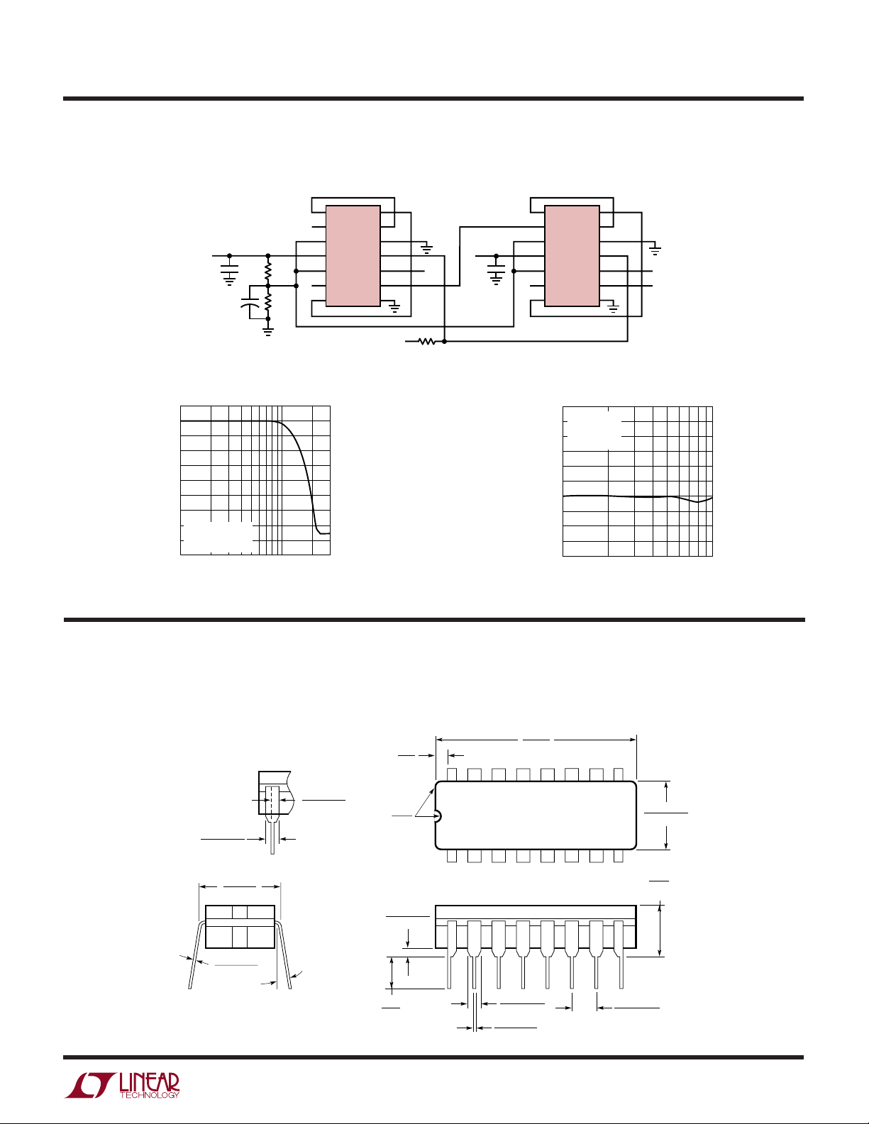
TYPICAL APPLICATIO
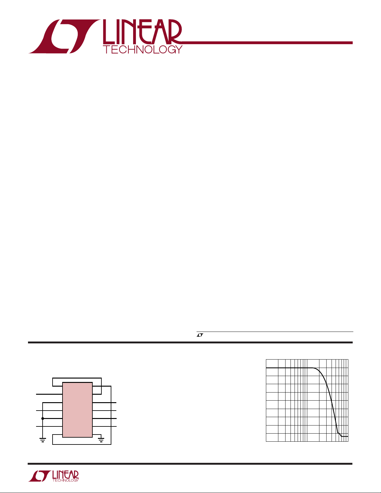
Butterworth 20kHz Anti-Aliasing Filter
1
V
IN
8V
NC
2
3
4
5
6
7
LTC1164-5
14
13
12
11
10
9
8
U
–8V
CLK = 1MHz
+
TO V
V
OUT
1164-5 TA01
WIDEBAND NOISE = 110µV
THD IN PASSBAND < 0.02% AT VIN = 2V
NOTE: THE CONNECTION FROM PIN 7 TO PIN 14
SHOULD BE MADE UNDER THE PACKAGE.
FOR 50:1 OPERATION CONNECT PIN 1 TO PIN 13
AS SHOWN. FOR 100:1 OR 150:1 OPERATION PINS 1
AND 13 SHOULD FLOAT. THE POWER SUPPLIES
SHOULD BE BYPASSED BY A 0.1µF CAPACITOR AS
CLOSE TO THE PACKAGE AS POSSIBLE.
RMS
RMS
0
–10
–20
–30
–40
GAIN (dB)
–50
–60
–70
–80
1
Frequency Response
10 100
FREQUENCY (kHz)
LTC1164-5 TA02
1
Page 2
LTC1164-5
WW
W
ABSOLUTE AXI U RATI GS
U
(Note 1)
Total Supply Voltage (V+ to V–) ............................. 16V
Input Voltage (Note 2) ......... (V++ 0.3V) to (V– – 0.3V)
Output Short Circuit Duration ......................... Indefinite
Power Dissipation............................................. 400mW
Burn-In Voltage ...................................................... 16V
UUW
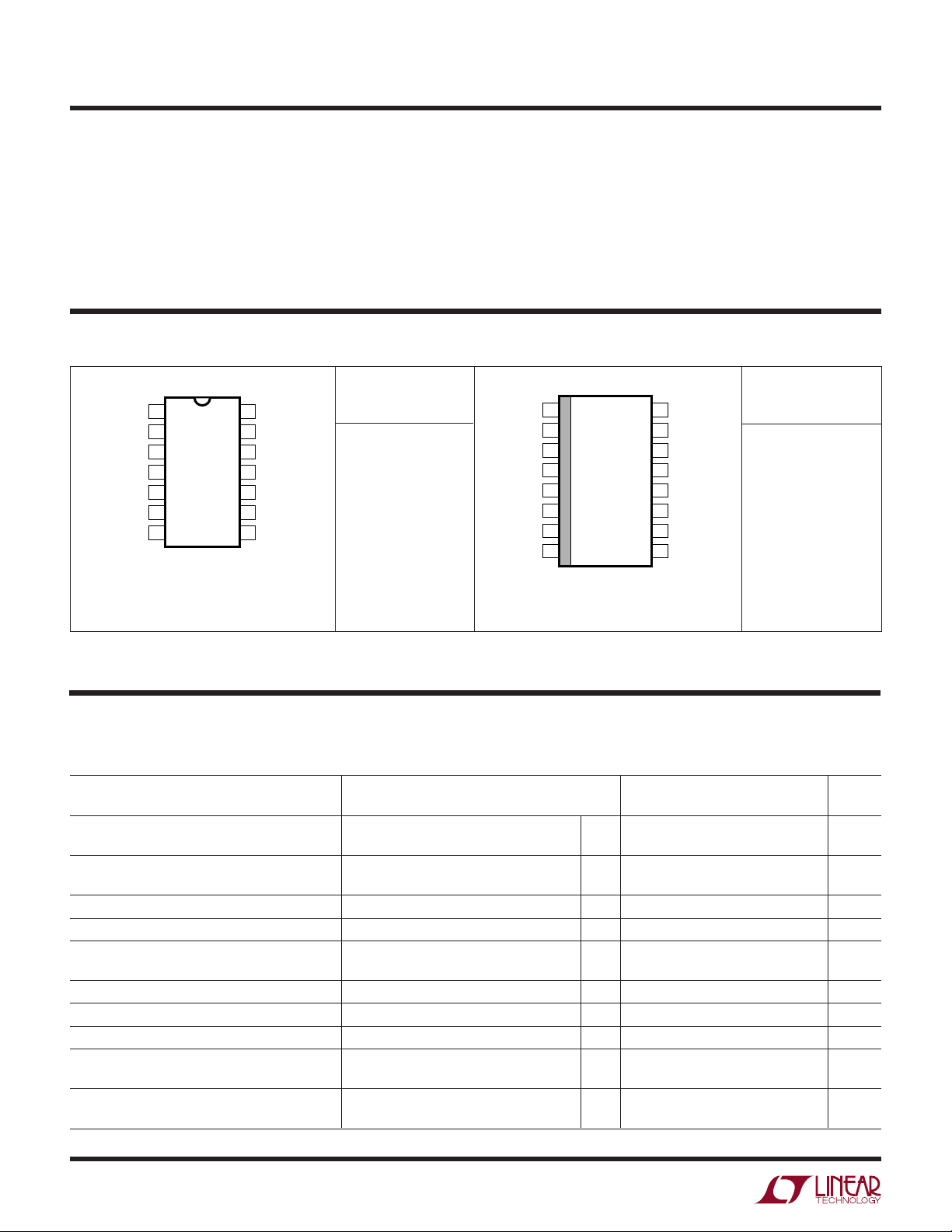
PACKAGE/ORDER I FOR ATIO
50:1 MODE
V
GND
V
GND
LP6
CONNECT 1
J PACKAGE
14-LEAD CERDIP
IN
+
T
T
JMAX
JMAX
1
2
3
4
5
6
7
= 150°C,
= 110°C,
TOP VIEW
θJA = 65°C/W (J)
θJA = 65°C/W (N)
CONNECT 2
14
50:1 MODE
13
–
V
12
CLK
11
BUTT/BESS
10
V
9
OUT
NC
8
N PACKAGE
14-LEAD PDIP
ORDER PART
NUMBER
LTC1164-5CN
LTC1164-5CJ
LTC1164-5MJ
Operating Temperature Range
LTC1164-5C ...................................... – 40°C to 85°C
LTC1164-5M .................................... –55°C to 125°C
Storage Temperature Range ................ –65°C to 150°C
Lead Temperature (Soldering, 10 sec)................. 300°C
50:1 MODE
V
GND
GND
NC
LP6
CONNECT 1
1
2
IN
3
+
4
V
5
6
7
8
16-LEAD PLASTIC SW
T
= 110°C,
JMAX
TOP VIEW
S PACKAGE
θJA = 85°C/W
16
15
14
13
12
11
10
9
CONNECT 2
50:1 MODE
–
V
NC
CLK
BUTT/BESS
NC
V
OUT
ORDER PART
NUMBER
LTC1164-5CS
Consult factory for Industrial grade parts.
ELECTRICAL CHARACTERISTICS
VS = ±7.5V, RL = 10k, f
PARAMETER CONDITIONS MIN TYP MAX UNITS
Passband Gain 0.1Hz at 0.25f
Gain at 0.50f
Gain at 0.90f
Gain at 0.95f
Gain at f
CUTOFF
Gain at 1.44f
Gain at 2.0f
Gain with f
Gain with VS = 2.375V (Note 3) fIN = 400kHz, fIN = 2kHz, (f
Input Frequency Range (f
(Note 3) fIN = 2kHz, (f
CUTOFF
(Note 3) fIN = 3.6kHz, (f
CUTOFF
(Note 3) fIN = 3.8kHz, (f
CUTOFF
(Note 3) fIN = 4kHz, (f
(Note 3) fIN = 5.76kHz, (f
CUTOFF
(Note 3) fIN = 8kHz, (f
CUTOFF
= 20kHz (Note 3) fIN = 200Hz, (f
CLK
= 400kHz, TA = Operating Temperature Range, unless otherwise specified.
CLK
(Note 3) fIN = 1kHz, (f
CUTOFF
f
= 1kHz, (f
IN
f
= 4kHz, (f
IN
= 8kHz, (f
f
IN
= 400kHz, fIN = 4kHz, (f
f
IN
) = 100:1 0 – <f
CLK/fC
) = 50:1 0 – <f
(f
CLK/fC
) = 100:1 ● –0.5 –0.10 0.25 dB
CLK/fC
) = 50:1 ● –0.5 0.10 0.25 dB
CLK/fC
) = 100:1 ● –0.45 –0.20 0.17 dB
CLK/fC
) = 50:1 ● –0.35 –0.10 0.40 dB
CLK/fC
) = 100:1 ● –2.50 –1.90 –1.0 dB
CLK/fC
) = 100:1 –2.60 dB
CLK/fC
) = 100:1 ● –4.10 –3.40 –2.75 dB
CLK/fC
) = 50:1 ● –4.20 –3.80 –2.75 dB
CLK/fC
) = 100:1 ● –20.5 –19.0 –17.0 dB
CLK/fC
) = 100:1 ● –45.0 –43.0 –41.0 dB
CLK/fC
) = 100:1 ● –4.50 –3.40 –2.75 dB
CLK/fC
) = 100:1 –0.50 –0.10 0.35 dB
CLK/fC
) = 100:1 –4.20 –3.40 –2.00 dB
CLK/fC
LTC1164-5C
/2 kHz
CLK
CLK
kHz
2
Page 3
LTC1164-5
ELECTRICAL CHARACTERISTICS
VS = ±7.5V, RL = 10k, f
PARAMETER CONDITIONS MIN TYP MAX UNITS
Maximum f
Clock Feedthrough Input at GND, f = f
Wideband Noise Input at GND, 1Hz ≥ f < f
Input Impedance 70 100 160 kΩ
Output DC Voltage Swing VS = ±2.375V ● ±1.25 ±1.50 V
Output DC Offset VS = ±5V, (f
Output DC Offset TempCo VS = ±5V, (f
Power Supply Current VS = ±2.375V, TA ≥ 25°C 2.5 4.0 mA
Power Supply Range ±2.375 ±8V
The ● denotes specifications which apply over the full operating
temperature range.
Note 1: Absolute Maximum Ratings are those values beyond which life of
the device may be impaired.
CLK
= 400kHz, TA = Operating Temperature Range, unless otherwise specified.
CLK
VS ≥ ±7.5V 1.5 MHz
= ±5.0V 1.0 MHz
V
S
= Single 5V (GND = 2V) 1.0 MHz
V
S
, Square Wave
CLK
±5V, (f
±5V, (f
±5V, (f
±5V, (f
V
= ±5.0V ● ±3.70 ±4.10 V
S
= ±7.5V ● ±5.40 ±5.90 V
V
S
= ±5.0V, TA ≥ 25°C 4.5 7.0 mA
V
S
= ±7.5V, TA ≥ 25°C 7.0 11.0 mA
V
S
) = 100:1 200 µV
CLK/fC
) = 50:1 100 µV
CLK/fC
) = 100:1 100 ±5% µV
CLK/fC
) = 50:1 115 ±5% µV
CLK/fC
CLK/fC
CLK/fC
CLK
) = 100:1 ±50 ±160 mV
) = 100:1 ±100 µV/°C
● 4.5 mA
● 8.0 mA
● 12.5 mA
Note 2: Connecting any pin to voltages greater than V
may cause latchup. It is recommended that no sources operating from
external supplies be applied prior to power-up of the LTC1164-5.
Note 3: All gains are measured relative to passband gain. The filter cutoff
frequency is abbreviated as f
CUTOFF
LTC1164-5C
or fC.
+
or less than V
RMS
RMS
RMS
RMS
–
UW
TYPICAL PERFOR A CE CHARACTERISTICS
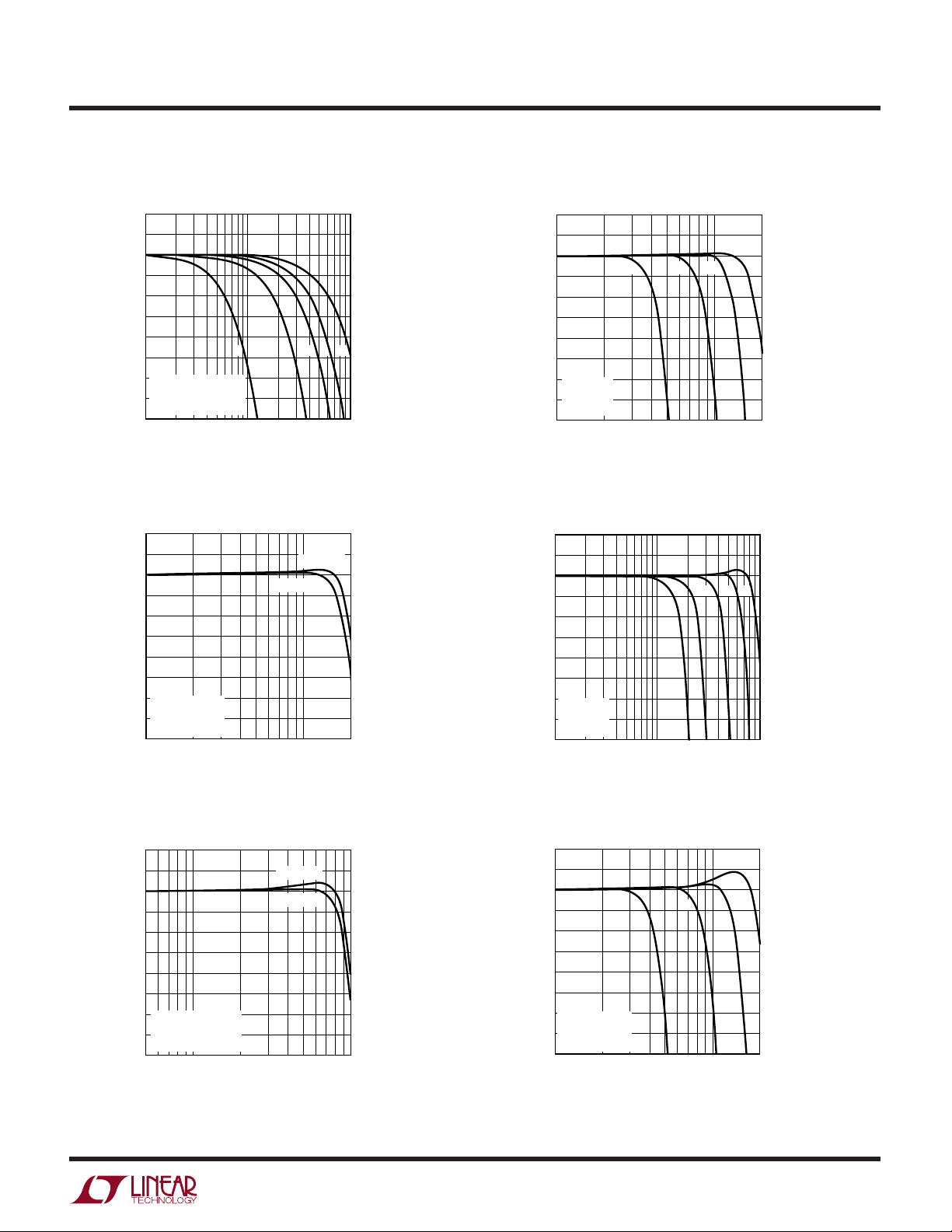
Gain vs Frequency
A. f
= 100kHz
CLK
f
0
–10
–20
–30
–40
GAIN (dB)
–50
–60
–70
–80
0.1
VS = ±5V
= 25°C
T
A
ACB
110
FREQUENCY (kHz)
LTC1164-5 • G01
50
= 1kHz
CUTOFF
(100:1, PIN 10 TO V–)
= 375kHz
B. f
CLK
f
= 2.68kHz
CUTOFF
(140:1, PIN 10 GND)
= 500kHz
C. f
CLK
= 10kHz
f
CUTOFF
(50:1, PIN 10 TO V+,
PINS 1-13 SHORTED)
Passband Gain and Phase
vs Frequency
0
–5
GAIN (dB)
–10
VS = ±5V
= 50kHz
f
CLK
= 1kHz
f
CUTOFF
–15
(50:1, PIN 10 TO V
PINS 1-13 SHORTED)
= 25°C
T
A
0.2
+
0.4
FREQUENCY (kHz)
0
GAIN
PHASE
,
0.8
0.6
1.0
LTC1164-5 • G02
–90
–180
–270
PHASE (DEG)
3
Page 4
LTC1164-5
FREQUENCY (kHz)
0.1
–4.0
GAIN (dB)
–3.5
–2.5
–2.0
–1.5
–0.5
1
10
LTC1164-5 • G06
–3.0
0
0.5
–1.0
AEFB C D
A. f
CLK
= 200kHz
f
CUTOFF
= 4kHz
B. f
CLK
= 300kHz
f
CUTOFF
= 6kHz
C. f
CLK
= 500kHz
f
CUTOFF
= 10kHz
D. f
CLK
= 750kHz
f
CUTOFF
= 15kHz
E. f
CLK
= 1MHz
f
CUTOFF
= 20kHz
F. f
CLK
= 1.5MHz
f
CUTOFF
= 30kHz
VS = ±7.5V
50:1
T
A
= 25°C
30
UW
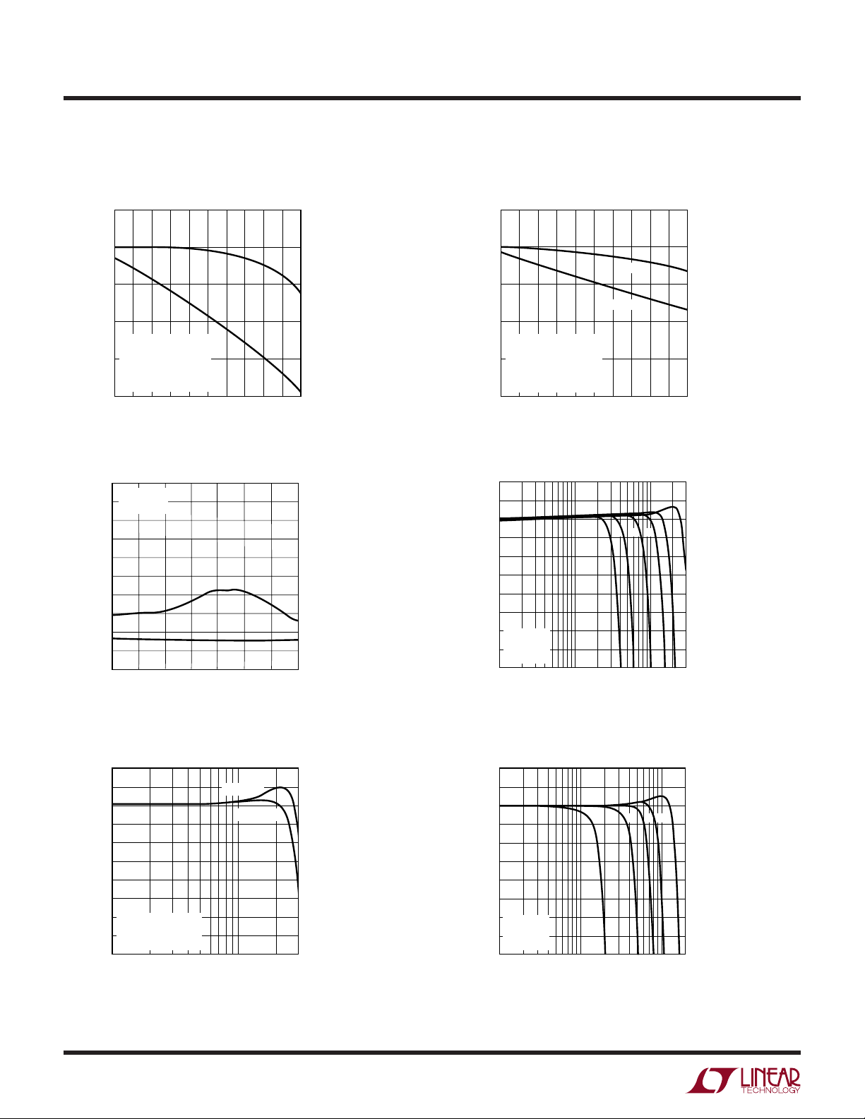
TYPICAL PERFOR A CE CHARACTERISTICS
Passband Gain and Phase
vs Frequency
0
–5
GAIN (dB)
–10
VS = ±5V
f
= 100kHz
CLK
–15
–20
= 1kHz
f
CUTOFF
(100:1, PIN 10 TO V
= 25°C
T
A
0.4
0.2
FREQUENCY (kHz)
Group Delay vs Frequency
500
VS = ±7.5V
450
= 25°C
T
A
400
350
300
250
200
A
GROUP DELAY (µs)
150
100
B
50
0
0.5
1.5
3.5
2.5
FREQUENCY (kHz)
–
0.6
Passband Gain and Phase
vs Frequency
0
PHASE (DEG)
–90
–180
–270
)
4.5
0.8
LTC1164-5 • G03
5.5
LTC1164-5 • G05
6.5
1.0
–360
= 500kHz
A. f
CLK
(BUTTERWORTH 100:1)
f
CUTOFF
= 750kHz
B. f
CLK
(BESSEL 140:1)
f
CUTOFF
7.5
= 5kHz
= 5.36kHz
0
–5
GAIN (dB)
–10
VS = ±5V
= 150kHz
f
CLK
–15
–20
= 1.07kHz
f
CUTOFF
(140:1, PIN 10 TO GND)
= 25°C
T
A
0.4
0.2
0.6
FREQUENCY (kHz)
Passband vs Frequency and f
GAIN
PHASE
0.8
1.0
LTC1164-5 • G04
CLK
0
PHASE (DEG)
–90
–180
–270
–360
4
Maximum Passband over
Temperature for VS = ±7.5V, 50:1 Passband vs Frequency and f
0.5
0
–0.5
–1.0
–1.5
GAIN (dB)
–2.0
–2.5
–3.0
VS = ±7.5V
= 1.5MHz (50:1)
f
CLK
–3.5
f
CUTOFF
–4.0
1
= 30kHz
FREQUENCY (kHz)
TA = 70°C
TA = –40°C
10
LTC1164-5 • G07
30
0.5
0
–0.5
–1.0
–1.5
GAIN (dB)
–2.0
–2.5
–3.0
–3.5
–4.0
0.1
VS = ±7.5V
100:1
= 25°C
T
A
A
1
FREQUENCY (kHz)
B C D
LTC1164-5 • G08
CLK
10
A. f
= 200kHz
CLK
= 2kHz
f
CUTOFF
= 500kHz
B. f
CLK
= 5kHz
f
CUTOFF
E
= 750kHz
C. f
CLK
= 7.5kHz
f
CUTOFF
= 1MHz
D. f
CLK
= 10kHz
f
CUTOFF
= 1.5MHz
E. f
CLK
= 15kHz
f
CUTOFF
20
Page 5
UW
TYPICAL PERFOR A CE CHARACTERISTICS
LTC1164-5
Passband vs Frequency and f
0.5
0
–0.5
–1.0
–1.5
GAIN (dB)
–2.0
–2.5
–3.0
VS = ±7.5V, 140:1
(BESSEL RESPONSE)
–3.5
= 25°C
T
A
–4.0
0.1
110
FREQUENCY (kHz)
Maximum Passband over
Temperature for VS = ±5V, 50:1
0.5
0
–0.5
–1.0
–1.5
GAIN (dB)
–2.0
–2.5
–3.0
VS = ±5V
= 1MHz
f
–3.5
CLK
= 20kHz
f
CUTOFF
–4.0
1
FREQUENCY (kHz)
B DA C E
LTC1164-5 • G09
TA = 70°C
TA = –40°C
10
LTC1164-5 • G011
CLK
Passband vs Frequency and f
A. f
= 150kHz
CLK
= 1.07kHz
f
B. f
C. f
D. f
E. f
CUTOFF
CLK
f
CUTOFF
CLK
f
CUTOFF
CLK
f
CUTOFF
CLK
f
CUTOFF
= 450kHz
= 3.21kHz
= 750kHz
= 5.36kHz
= 1MHz
= 7.14kHz
= 1.5MHz
= 10.71kHz
0.5
0
–0.5
–1.0
–1.5
GAIN (dB)
–2.0
–2.5
–3.0
–3.5
–4.0
1
VS = ±5V
50:1
= 25°C
T
A
A B C D
FREQUENCY (kHz)
Passband vs Frequency and f
0.5
0
–0.5
–1.0
–1.5
GAIN (dB)
–2.0
–2.5
–3.0
VS = ±5V
100:1
–3.5
= 25°C
T
A
20
–4.0
0.1
A
B
110
FREQUENCY (kHz)
CLK
10
LTC1164-5 • G10
CLK
DC E
LTC1164-5 • G12
A. f
= 250kHz
CLK
= 5kHz
f
CUTOFF
= 500kHz
B. f
CLK
= 10kHz
f
CUTOFF
= 750kHz
C. f
CLK
= 15kHz
f
CUTOFF
= 1MHz
D. f
CLK
= 20kHz
f
CUTOFF
20
A. f
= 200kHz
CLK
= 2kHz
f
CUTOFF
= 300kHz
B. f
CLK
= 3kHz
f
CUTOFF
= 500kHz
C. f
CLK
= 5kHz
f
CUTOFF
= 750kHz
D. f
CLK
= 7.5kHz
f
CUTOFF
= 1MHz
E. f
CLK
= 10kHz
f
CUTOFF
Maximum Passband over
Temperature for VS = ±5V, 100:1 Passband vs Frequency and f
0.5
0
–0.5
–1.0
–1.5
GAIN (dB)
–2.0
–2.5
–3.0
–3.5
–4.0
0.5
TA = –40°C
VS = ±5V
= 1MHz (100:1)
f
CLK
= 10kHz
f
CUTOFF
1 10
FREQUENCY (kHz)
TA = 70°C
LTC1164-5 • G13
0.5
0
–0.5
–1.0
–1.5
GAIN (dB)
–2.0
–2.5
–3.0
–3.5
–4.0
1
VS = SINGLE 5V
50:1
= 25°C
T
A
FREQUENCY (kHz)
A
B
CLK
C
10
LTC1164-5 • G14
A. f
= 250kHz
CLK
= 5kHz
f
CUTOFF
= 500kHz
B. f
CLK
= 10kHz
f
CUTOFF
D
= 750kHz
C. f
CLK
= 15kHz
f
CUTOFF
= 1MHz
D. f
CLK
= 20kHz
f
CUTOFF
20
5
Page 6
LTC1164-5
UW
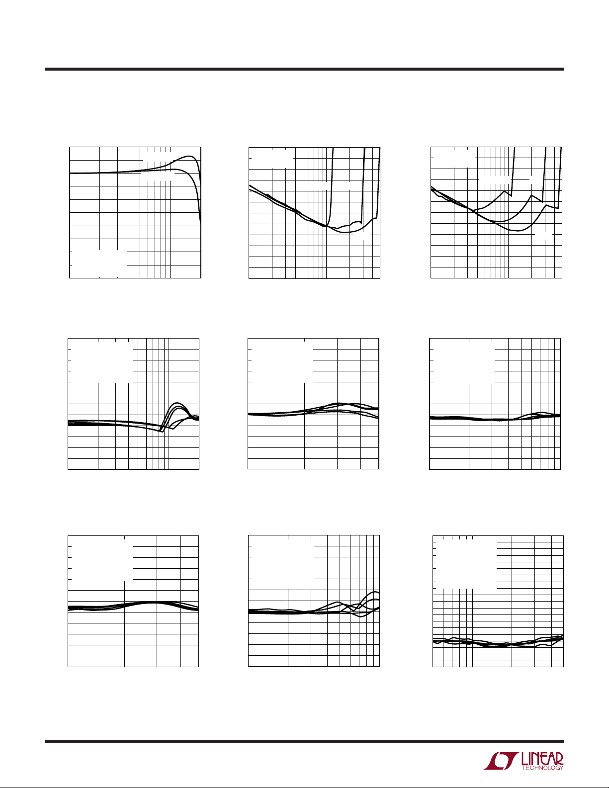
TYPICAL PERFOR A CE CHARACTERISTICS
Maximum Passband over
Temperature for Single 5V, 50:1* THD + Noise vs RMS Input, 100:1THD + Noise vs RMS Input, 50:1
–40
0.5
0
–0.5
–1.0
–1.5
GAIN (dB)
–2.0
–2.5
–3.0
VS = SINGLE 5V
f
CLK
–3.5
f
CUTOFF
–4.0
1
–40
VIN = 2V
±7.5V, 50:1
–50
f
CLK
(5 REPRESENTATIVE
UNITS)
–60
TA = 70°C
TA = –40°C
= 1MHz (50:1)
= 20kHz
10
FREQUENCY (kHz)
LTC1164-5 • G015
RMS
= 1MHz
fIN = 1kHz
= 500kHz
f
CLK
–50
–60
–70
–80
THD + NOISE (dB)
–90
–100
0.1
–40
VIN = 2V
±7.5V, 100:1
–50
–60
= 500kHz
f
CLK
(5 REPRESENTATIVE
UNITS)
SINGLE 5V ±5V
15
FREQUENCY (kHz)
RMS
±7.5V
LTC1164-5 • G16
–40
fIN = 1kHz
= 500kHz
f
CLK
–50
–60
–70
–80
THD + NOISE (dB)
–90
–100
0.1
THD + Noise vs FrequencyTHD + Noise vs Frequency THD + Noise vs Frequency
–40
VIN = 1V
±5V, 50:1
–50
–60
= 500kHz
f
CLK
(5 REPRESENTATIVE
UNITS)
SINGLE 5V ±5V
±7.5V
15
FREQUENCY (kHz)
LTC1164-5 • G17
RMS
–70
–80
THD + NOISE (dB)
–90
–100
1
–40
VIN = 1V
±5V, 100:1
–50
–60
–70
–80
THD + NOISE (dB)
–90
–100
= 500kHz
f
CLK
(5 REPRESENTATIVE
UNITS)
1
FREQUENCY (kHz)
RMS
25
FREQUENCY (kHz)
10 20
LTC1164-5 • G18
34
LTC1164-5 • G21
–70
–80
THD + NOISE (dB)
–90
–100
1
–40
VIN = 0.7V
SINGLE 5V SUPPLY
–50
50:1, f
CLK
= 10kHz
f
C
(5 REPRESENTATIVE
–60
UNITS)
–70
–80
THD + NOISE (dB)
–90
–100
1
25
FREQUENCY (kHz)
RMS
= 500kHz
FREQUENCY (kHz)
34
LTC1164-5 • G19
5
LTC1164-5 • G22
10
–70
–80
THD + NOISE (dB)
–90
–100
1
THD + Noise vs FrequencyTHD + Noise vs Frequency THD + Noise vs Frequency
–50
VIN = 2V
–54
VS = ±7.5V, 140:1
= 750kHz
f
CLK
–58
= 5.36kHz
f
C
–62
(5 REPRESENTATIVE
UNITS)
–66
–70
–74
THD + NOISE (dB)
–78
–82
–86
–90
0.5
FREQUENCY (kHz)
RMS
1
FREQUENCY (kHz)
5
LTC1164-5 • G20
10
5
LTC1164-5 • G23
* See also Passband vs Frequency and f
for Single 5V, 50:1; THD + Noise vs RMS Input for Single 5V, 50:1;
CLK
and Maximum Passband for Single 5V, 50:1, for Two Ground Bias Levels.
6
Page 7
UW
TYPICAL PERFOR A CE CHARACTERISTICS
LTC1164-5
THD + Noise vs Input Voltage
–50
fIN = 1kHz, 140:1
–54
–58
–62
–66
–70
–74
–78
–82
THD + WIDEBAND NOISE (dB)
–86
–90
= 750kHz
f
CLK
VS = ±2.5V
0.1
INPUT VOLTAGE (V
10
MAXIMUM PHASE DIFFERENCE
BETWEEN ANY TWO UNITS
(SAMPLE OF 50 UNITS)
8
V
S
T
A
f
CLK
6
4
2
TOTAL PHASE DIFFERENCE (DEG)
0
0
VS = ±5V
≥ ±5V
≤ 70°C
≤ 500KHz
0.2
FREQUENCY (FREQUENCY/f
VS = ±7.5V
1
)
RMS
LTC1164-5 • G24
0.4 0.6 0.8
5
A
B
CUTOFF
LTC1164-5 • G27
2.0
1.5
1.0
0.5
–0.5
–1.0
PHASE (DEG)
–1.5
–2.0
–2.5
–3.0
1.0 1.2
)
Maximum Passband for Single 5V,
50:1, for Two Ground Bias Levels
TA = 70°C
= 1MHz
f
CLK
GND = 2.5V
0
GND = 2V
6
2
A. BUTTERWORTH
(f
B. BESSEL (f
84
FREQUENCY (kHz)
CLK/fCUTOFF
CLK/fCUTOFF
10
= 100:1 OR 50:1)
= 140:1)
16
LTC1164-5 • TPC25
18
201412
PSRR (dB)
THD + Noise vs RMS Input for
Single 5V, 50:1
–40
f
= 1MHz
CLK
–45
=25°C
T
A
–50
–55
–60
–65
–70
THD + NOISE (dB)
–75
–80
–85
22
–90
0.50
0.75 1.00
Power Supply Rejection Ratio
vs FrequencyPhase Matching vs Frequency
10
f
= 1kHz
CUTOFF
0
–10
–20
–30
–40
–50
–60
–70
–80
–90
20
100
1k
FREQUENCY (Hz)
GND = 2V
GND = 2.5V
INPUT (V
V
V
10k
LTC1164-5 • G28
RMS
+
–
1.25
)
50k
1.50
LTC1164-5 G26
Power Supply Current vs Power
Supply Voltage
12
11
10
9
8
7
6
5
CURRENT (mA)
4
3
2
1
0
13 68
0
POWER SUPPLY (V+ OR V–)
–55°C
25°C
125°C
LTC1164-5 • G29
1024579
Transient Response
VIN = ±3V, 500Hz Square Wave
2V/DIV
500µs/DIV
BUTTERWORTH RATIO = 100:1
f
= 500kHz
CLK
f
= 5kHz
C
V
= ±7.5V
S
1164-5 G30
Transient Response
VIN = ±3V, 500Hz Square Wave
2V/DIV
500µs/DIV
BESSEL RATIO = 140:1
= 700kHz
f
CLK
f
= 5kHz
C
V
= ±7.5V
S
1164-5 G31
7
Page 8

LTC1164-5
UUU
PI FU CTIO S
Power Supply (Pins 4, 12)
The V+ (Pin 4) and the V– (Pin 12) should be bypassed with
a 0.1µF capacitor to an adequate analog ground. The
filter’s power supplies should be isolated from other
digital or high voltage analog supplies. A low noise linear
supply is recommended. Using a switching power supply
will lower the signal-to-noise ratio of the filter. The supply
during power-up should have a slew rate less than 1V/µs.
When V+ is applied before V–, and V– can be more positive
than ground, a signal diode must be used to clamp V–.
Figures 1 and 2 show typical connections for dual and
single supply operation.
–
V
*
1k
V
OUT
CLK/fCUTOFF
CLOCK SOURCE
GND
DIGITAL SUPPLY
+
1164-5 F01
= 100:1
V
IN
+
V
0.1µF
* OPTIONAL (SEE TEXT)
1
2
3
4
5
6
7
LTC1164-5
14
13
0.1µF
12
11
10
9
8
Figure 1. Dual Supply Operation for f
Clock Input (Pin 11)
Any TTL or CMOS clock source with a square-wave output
and 50% duty cycle (±10%) is an adequate clock source
for the device. The power supply for the clock source
should not be the filter’s power supply. The analog ground
for the filter should be connected to clock’s ground at a
single point only. Table 1 shows the clock’s low and high
level threshold value for a dual or single supply operation.
A pulse generator can be used as a clock source provided
the high level ON time is greater than 0.5µs. Sine waves are
not recommended for clock input frequencies less than
100kHz, since excessively slow clock rise or fall times
generate internal clock jitter (maximum clock rise or fall
time ≤1µs). The clock signal should be routed from the
right side of the IC package to avoid coupling into any input
or output analog signal path. A 1k resistor between clock
source and Pin 11 will slow down the rise and fall times of
the clock to further reduce charge coupling, Figures 1
and 2.
Table 1. Clock Source High and Low Threshold Levels
POWER SUPPLY HIGH LEVEL LOW LEVEL
Dual Supply > ±3.4V ≥ V+/3 ≤ 0.5V
Dual Supply ≤ ±3.4V ≥ V+/3 ≤ V– + 0.5V
Single Supply V+ > 6.8V, V– = 0V ≥ V+• 0.65 ≤ 0.5V + 1/2V
Single Supply V+ < 6.8V, V– = 0V ≥ V+/3 ≤ 0.5V
+
1
V
5V ≤ V+ ≤ 16V
IN
0.1µF
10k
10k
2
3
4
LTC1164-5
5
6
7
+
1µF
Figure 2. Single Supply Operation for f
8
14
13
12
1k
11
10
9
8
CLK/fCUTOFF
CLOCK SOURCE
GND
DIGITAL SUPPLY
+
V
OUT
1164-5 F02
= 100:1
Analog Ground (Pins 3, 5)
The filter performance depends on the quality of the
analog signal ground. For either dual or single supply
operation, an analog ground plane surrounding the package is recommended. The analog ground plane should be
connected to any digital ground at a single point. For dual
supply operation, Pins 3 and 5 should be connected to the
analog ground plane. For single supply operation Pins 3
and 5 should be biased at 1/2 supply and they should be
bypassed to the analog ground plane with at least a 1µF
capacitor (Figure 2). For single 5V operation at the highest
f
of 1MHz, Pins 3 and 5 should be biased at 2V. This
CLK
minimizes passband gain and phase variations (see Typical Performance Characteristics curves: Maximum Passband for Single 5V, 50:1; and THD + Noise vs RMS Input
for Single 5V, 50:1).
Page 9

1k
1164-5 F03
–
+
LT1056
UUU
PI FU CTIO S
LTC1164-5
Butterworth/Bessel (Pin 10)
The DC level at Pin 10 determines the ratio of the clock
frequency to the cutoff frequency of the filter. Pin 10 at V
+
gives a 50:1 ratio and a Butterworth response (pins 1 to 13
are shorted for 50:1 only). Pin 10 at V– gives a 100:1
Butterworth response. Pin 10 at ground gives a Bessel
response and a ratio of 140:1. For single supply operation
the ratio is 50:1 when Pin 10 is at V+ (pins 1 to 13 shorted),
100:1 when Pin 10 is at ground, and 140:1 when at 1/2
supply. When Pin 10 is not tied to ground, it should be
bypassed to analog ground with a 0.1µF capacitor. If the
DC level at Pin 10 is switched mechanically or electrically
at slew rates greater than 1V/µs while the device is
operating, a 10k resistor should be connected between
Pin␣ 10 and the DC source.
Filter Input (Pin 2)
The input pin is connected internally through a 100k
resistor tied to the inverting input of an op amp.
Filter Output (Pins 9, 6)
Pin 9 is the specified output of the filter; it can typically
source or sink 1mA. Driving coaxial cables or resistive
loads less than 20k will degrade the total harmonic distortion of the filter. When evaluating the device’s distortion an
output buffer is required. A noninverting buffer, Figure 3,
can be used provided that its input common mode range
is well within the filter’s output swing. Pin 6 is an intermediate filter output providing an unspecified 6th order
lowpass filter. Pin 6 should not be loaded.
Figure 3. Buffer for Filter Output
External Connection (Pins 7, 14 and 1, 13)
Pins 7 and 14 should be connected together. In a printed
circuit board the connection should be done under the IC
package through a short trace surrounded by the analog
ground plane. When the clock to cutoff frequency ratio is
set at 50:1, Pin 1 should be shorted to Pin 13; if not, the
passband will exhibit 1dB of gain peaking and it will deviate
from a Butterworth response. Pin 1 is the inverting input
of an internal op amp and it should preferably be 0.2 inches
away from any other circuit trace.
NC (Pin 8)
Pin 8 is not connected to any internal circuit point on the
device and should be preferably tied to analog ground.
U
WUU
APPLICATIO S I FOR ATIO
Clock Feedthrough
Clock feedthrough is defined as, the RMS value of the
clock frequency and its harmonics that are present at the
filter’s output pin (Pin 9). The clock feedthrough is tested
with the input pin (Pin 2) grounded and, it depends on PC
board layout and on the value of the power supplies. With
proper layout techniques the values of the clock feedthrough
are shown in Table 2.
Table 2. Output Clock Feedthrough
V
S
±2.5V 60µV
±5V 100µV
±7.5V 150µV
Note: The clock feedthrough at ±2.5V supplies is imbedded in the
wideband noise of the filter. The clock waveform is a square wave.
50:1 100:1
RMS
RMS
RMS
60µV
200µV
500µV
RMS
RMS
RMS
9
Page 10
LTC1164-5
U
WUU
APPLICATIO S I FOR ATIO
Any parasitic switching transients during the rise and fall
edges of the incoming clock are not part of the clock
feedthrough specifications. Switching transients have frequency contents much higher than the applied clock; their
amplitude strongly depends on scope probing techniques
as well as grounding and power supply bypassing. The
clock feedthrough, if bothersome, can be greatly reduced
by adding a simple R/C lowpass network at the output of
the filter pin (Pin 9). This R/C will completely eliminate any
switching transient.
Wideband Noise
The wideband noise of the filter is the total RMS value of
the device’s noise spectral density and it is used to
determine the operating signal-to-noise ratio. Most of its
frequency contents lie within the filter passband and it
cannot be reduced with post filtering. For instance, the
LTC1164-5 wideband noise at ±2.5V supply is 100µV
95µV
of which have frequency contents from DC up to
RMS
the filter’s cutoff frequency. The total wideband noise
(µRMS) is nearly independent of the value of the clock. The
clock feedthrough specifications are not part of the wideband noise.
Speed Limitations
The LTC1164-5 optimizes AC performance versus power
consumption. To avoid op amp slew rate limiting at
maximum clock frequencies, the signal amplitude should
be kept below a specified level as shown in Table 3.
Table 3. Maximum VIN vs VS and f
POWER SUPPLY MAXIMUM f
VS = ±7.5V 1.5MHz 1V
VS = ±7.5V 1.0MHz 3V
VS = ±5.0V 1.0MHz 2.5V
Single 5V 1.0MHz 0.7V
CLK
CLK
MAXIMUM V
RMS
0.5V
RMS
RMS
0.7V
RMS
RMS
0.5V
RMS
RMS
0.5V
RMS
IN
(fIN > 35kHz)
(fIN > 250kHz)
(fIN > 25kHz)
(fIN > 250kHz)
(fIN > 25kHz)
(fIN > 100kHz)
(fIN > 25kHz)
(fIN > 100kHz)
RMS
,
Aliasing
Aliasing is an inherent phenomenon of sampled data
systems and it occurs when input frequencies close to the
sampling frequency are applied. For the LTC1164-5 case
at 100:1, an input signal whose frequency is in the range
of f
±2.5% will be aliased back into the filter’s pass-
CLK
band. If, for instance, an LTC1164-5 operating with a
100kHz clock and 1kHz cutoff frequency receives a 98kHz
10mV input signal, a 2kHz 56µV alias signal will appear at
its output. When the LTC1164-5 operates with a clock-tocutoff frequency of 50:1, aliasing occurs at twice the clock
frequency. Table 4 shows details.
Table 4. Aliasing Data (f
INPUT FREQUENCY OUTPUT LEVEL OUTPUT FREQUENCY
= 1V
(V
IN
(f
CLK/fC
97.0kHz –102.0dB 3.0kHz
97.5kHz –65.0dB 2.5kHz
98.0kHz –45.0dB 2.0kHz
98.5kHz –23.0dB 1.5kHz
99.0kHz –4.0dB 1.0kHz
99.5kHz –0.3dB 0.5kHz
(f
CLK/fC
197.0kHz –23.0dB 3.0kHz
197.5kHz –12.0dB 2.5kHz
198.0kHz –5.0dB 2.0kHz
198.5kHz –1.8dB 1.5kHz
199.0kHz –1.0dB 1.0kHz
199.5kHz –0.8dB 0.5kHz
) (Relative to Input) (Aliased Frequency)
RMS
) = 100:1, f
) = 50:1, f
CUTOFF
CUTOFF
Table 5. Transient Response of LTC Lowpass Filters
LOWPASS FILTER (SEC) (SEC) (SEC) (%)
LTC1064-3 Bessel 0.50/f
LTC1164-5 Bessel 0.43/f
LTC1164-6 Bessel 0.43/f
LTC1264-7 Linear Phase 1.15/fC0.36/f
LTC1164-7 Linear Phase 1.20/f
LTC1064-7 Linear Phase 1.20/f
LTC1164-5 Butterworth 0.80/fC0.48/f
LTC1164-6 Elliptic 0.85/f
LTC1064-4 Elliptic 0.90/fC0.54/f
LTC1064-1 Elliptic 0.85/f
* To 50% ±5%, ** 10% to 90% ±5%, *** To 1% ±0.5%
= 100kHz, VS = ±5V)
CLK
= 1kHz
= 2kHz
DELAY RISE SETTLING OVER-
TIME* TIME** TIME*** SHOOT
0.34/f
C
0.34/f
C
0.34/f
C
0.39/f
C
0.39/f
C
0.54/f
C
0.54/f
C
0.80/f
C
0.85/f
C
1.15/f
C
2.05/f
C
2.20/f
C
2.20/f
C
2.40/f
C
4.30/f
C
4.50/f
C
6.50/f
C
0.5
C
C
C
C
C
C
C
C
C
C
0
1
5
5
5
11
18
20
20
10
Page 11
U
TYPICAL APPLICATIO S
Single 5V, IS = 5.2mA, 16th Order Clock-Tunable Lowpass Filter,
f
CLK/fCUTOFF
= 60:1, –75dB Attenuation at 2.3 f
LTC1164-5
CUTOFF
5V
Gain vs Frequency
10
0
–10
–20
–30
–40
GAIN (dB)
–50
–60
–70
VS = SINGLE 5V
= 600kHz
f
CLK
–80
f
= 10kHz
CUTOFF
–90
1
0.1µF
15k
+
1µF
FREQUENCY (kHz)
10k
10
V
IN
LTC1164-5 • TA03
1
2
3
4
5
6
7
LTC1164-5
30
14
13
12
11
IC1
10
9
8
1k
f
CLK
5V
0.1µF
5V
1
2
3
4
5
6
7
LTC1164-5
IC2
14
13
12
11
10
9
8
5V
V
1164-5 F04
OUT
THD + Noise vs Frequency
–40
VS = SINGLE 5V
–45
= 0.5V
V
IN
RMS
f
= 600kHz
–50
CLK
= 10kHz
f
C
–55
–60
–65
–70
THD + NOISE (dB)
–75
–80
–85
–90
1
FREQUENCY (kHz)
5
LTC1164-5 • TA04
10
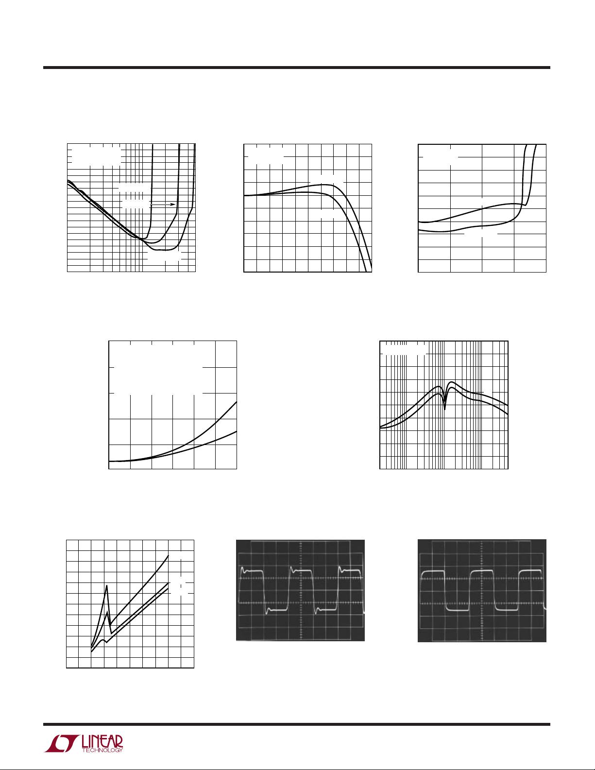
PACKAGE DESCRIPTIO
CORNER LEADS OPTION
(4 PLCS)
0.045 – 0.068
(1.143 – 1.727)
FULL LEAD
OPTION
0.300 BSC
(0.762 BSC)
0.008 – 0.018
(0.203 – 0.457)
NOTE: LEAD DIMENSIONS APPLY TO SOLDER DIP/PLATE
OR TIN PLATE LEADS
U
Dimensions in inches (millimeters) unless otherwise noted.
J Package
14-Lead CERDIP (Narrow 0.300, Hermetic)
(LTC DWG # 05-08-1110)
0.840
(21.336)
13
0.045 – 0.068
(1.143 – 1.727)
0.014 – 0.026
(0.360 – 0.660)
MAX
11121415
6
0.023 – 0.045
(0.584 – 1.143)
HALF LEAD
OPTION
0° – 15°
0.005
(0.127)
MIN
0.025
(0.635)
RAD TYP
0.015 – 0.060
(0.380 – 1.520)
0.125
(3.175)
MIN
16
2345
1
10
9
78
0.100 ± 0.010
(2.540 ± 0.254)
0.220 – 0.310
(5.588 – 7.874)
0.200
(5.080)
MAX
J16 1197
Information furnished by Linear Technology Corporation is believed to be accurate and reliable.
However, no responsibility is assumed for its use. Linear Technology Corporation makes no representation that the interconnection of its circuits as described herein will not infringe on existing patent rights.
11
Page 12
LTC1164-5
U
TYPICAL APPLICATIO S
8th Order Butterworth Lowpass Filter
f
= 50:1
CLK/fC
0.1µF
1
2
V
IN
3
+
V
4
5
6
7
LTC1164-5
+
14
13
12
11
f
CLK
10
V
9
V
8
+
OUT
–
V
0.1µF
1164-5 TA05
PACKAGE DESCRIPTIO
0.300 – 0.325
(7.620 – 8.255)
0.009 – 0.015
(0.229 – 0.381)
+0.035
0.325
–0.015
+0.889
8.255
()
–0.381
*THESE DIMENSIONS DO NOT INCLUDE MOLD FLASH OR PROTRUSIONS.
MOLD FLASH OR PROTRUSIONS SHALL NOT EXCEED 0.010 INCH (0.254mm)
0.291 – 0.299**
(7.391 – 7.595)
0.010 – 0.029
(0.254 – 0.737)
0.020
(0.508)
× 45°
MIN
0.130 ± 0.005
(3.302 ± 0.127)
0.125
(3.175)
MIN
8th Order Butterworth Lowpass Filter
f
= 100:1
CLK/fC
0.1µF
1
2
V
IN
3
+
V
+
4
5
6
7
LTC1164-5
14
13
12
11
f
CLK
10
9
V
OUT
8
–
V
0.1µF
1164-5 TA06
8th Order Linear Phase Lowpass Filter
U
Dimensions in inches (millimeters) unless otherwise noted.
N Package
14-Lead PDIP (Narrow 0.300)
(LTC DWG # 05-08-1510)
0.045 – 0.065
(1.143 – 1.651)
0.255 ± 0.015*
0.065
(6.477 ± 0.381)
(1.651)
TYP
0.005
(0.125)
MIN
0.100 ± 0.010
(2.540 ± 0.254)
0.018 ± 0.003
(0.457 ± 0.076)
SW Package
16-Lead Plastic Small Outline (Wide 0.300)
(LTC DWG # 05-08-1620)
0.093 – 0.104
(2.362 – 2.642)
0.037 – 0.045
(0.940 – 1.143)
14
15 1413121110 9
16
V
IN
0.1µF
+
V
1213
31
2
0.398 – 0.413*
(10.109 – 10.490)
f
CLK/fC
1
2
3
4
5
6
7
0.770*
(19.558)
MAX
11
4
= 140:1
LTC1164-5
5
14
13
12
11
f
CLK
10
9
8
6
N14 1197
–
V
0.1µF
V
OUT
1164-5 TA07
8910
7
° – 8° TYP
0
0.050
0.009 – 0.013
(0.229 – 0.330)
NOTE:
1. PIN 1 IDENT, NOTCH ON TOP AND CAVITIES ON THE BOTTOM OF PACKAGES ARE THE MANUFACTURING OPTIONS.
THE PART MAY BE SUPPLIED WITH OR WITHOUT ANY OF THE OPTIONS
DIMENSION DOES NOT INCLUDE MOLD FLASH. MOLD FLASH SHALL NOT EXCEED 0.006" (0.152mm) PER SIDE
*
DIMENSION DOES NOT INCLUDE INTERLEAD FLASH. INTERLEAD FLASH SHALL NOT EXCEED 0.010" (0.254mm) PER SIDE
**
NOTE 1
0.016 – 0.050
(0.406 – 1.270)
(1.270)
TYP
0.014 – 0.019
(0.356 – 0.482)
TYP
0.004 – 0.012
(0.102 – 0.305)
NOTE 1
2345
1
6
78
0.394 – 0.419
(10.007 – 10.643)
S16 (WIDE) 0396
RELATED PARTS
PART NUMBER DESCRIPTION COMMENTS
LTC1069-1 Low Power, 8th Order Elliptic Lowpass Filter Operates from a Single 3.3V to ±5V Supply
LTC1069-6 Very Low Power, 8th Order Elliptic Lowpass Filter Optimized for 3V/5V Single Supply Operation, Consumes 1mA at 3V
11645as, sn11645 LT/TP 1098 2K REV A • PRINTED IN USA
LINEAR TECHNOLOGY CORPORAT ION 1993
12
Linear Technology Corporation
1630 McCarthy Blvd., Milpitas, CA 95035-7417
(408) 432-1900 ● FAX: (408) 434-0507
●
www.linear-tech.com
 Loading...