

Datasheet LTC1159IS-5, LTC1159IS-3.3, LTC1159IS, LTC1159CS-5, LTC1159CS-3.3 Datasheet (Linear Technology)
...Page 1
FEATURES
■
Operation from 4V to 40V Input Voltage
■
Ultrahigh Efficiency: Up to 95%
■
20µA Supply Current in Shutdown
■
High Efficiency Maintained Over Wide Current Range
■
Current Mode Operation for Excellent Line and Load
Transient Response
■
Very Low Dropout Operation: 100% Duty Cycle
■
Short-Circuit Protection
■
Synchronous FET Switching for High Efficiency
■
Adaptive Non-Overlap Gate Drives
■
Available in SSOP and SO Packages
U
APPLICATIO S
■
Step-Down and Inverting Regulators
■
Notebook and Palmtop Computers
■
Portable Instruments
■
Battery-Operated Digital Devices
■
Industrial Power Distribution
■
Avionics Systems
■
Telecom Power Supplies
LTC1159
LTC1159-3.3/LTC1159- 5
High Efficiency Synchronous
Step-Down Switching Regulators
U
DESCRIPTIO
The LTC®1159 series is a family of synchronous step-down
switching regulator controllers featuring automatic Burst
ModeTM operation to maintain high efficiencies at low
output currents. These devices drive external complementary power MOSFETs at switching frequencies up to 250kHz
using a constant off-time current-mode architecture.
A separate pin and on-board switch allow the MOSFET
driver power to be derived from the regulated output
voltage providing significant efficiency improvement when
operating at high input voltages. The constant off-time
current-mode architecture maintains constant ripple current in the inductor and provides excellent line and load
transient response. The output current level is user programmable via an external current sense resistor.
The LTC1159 automatically switches to power saving
Burst Mode operation when load current drops below
approximately 15% of maximum current. Standby current
is only 300µA while still regulating the output and shut-
down current is a low 20µA.
, LTC and LT are registered trademarks of Linear Technology Corporation.
Burst Mode is a trademark of Linear Technology Corporation.
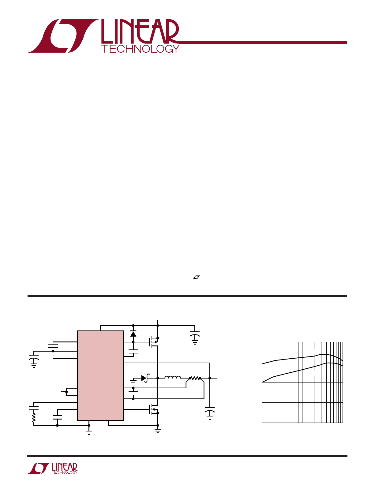
TYPICAL APPLICATIO
V
IN
+
3.3µF
0V = NORMAL
>2V = SHUTDOWN
3300pF
1k
C
T
300pF
CAP
V
CC
V
CC
SHDN1
SHDN2
I
TH
C
T
S-GND
0.15µF
Figure 1. High Efficiency Step-Down Regulator
P-GATE
P-DRIVE
EXTV
LTC1159-5
SENSE
SENSE
N-GATE
P-GND
U
V
IN
+
C
R
SENSE
0.05Ω
IN
100µF
100V
21
4
+
V
OUT
5V/2A
C
OUT
220µF
100
FIGURE 1 CIRCUIT
90
80
EFFICIENCY (%)
70
60
0.02
LTC1159-5 Efficiency
VIN = 10V
VIN = 20V
0.2 2
LOAD CURRENT (A)
LTC1159 • TA01
1N4148
Si9435DY
0.1µF
CC
+
–
D1
MBRS140T3
0.01µF
LTC1159 • F01
L*
33µH
3
Si9410DY
*COILTRONICS CTX33-4-MP
1
Page 2
LTC1159
LTC1159-3.3/LTC1159-5
A
W
O
LUTEXI TIS
S
A
WUW
U
ARB
G
(Note 1)
Input Supply Voltage (Pin 2) ..................... –15V to 60V
VCC Output Current (Pin 3) .................................. 50mA
Continuous Pin Currents (Any Pin)...................... 50mA
Sense Voltages ......................................... –0.3V to 13V
Shutdown Voltages................................................... 7V
EXTVCC Input Voltage ............................................. 15V
Junction Temperature (Note 2)............................ 125°C
WU
/
PACKAGE
P-GATE
V
IN
V
CC
P-DRIVE
P-DRIVE
V
CC
V
CC
C
T
I
TH
–
SENSE
T
O
RDER I FOR ATIO
TOP VIEW
1
2
3
4
5
6
7
8
9
10
G PACKAGE
20-LEAD PLASTIC SSOP
JMAX
= 125°C, θ
= 135°C/W
JA
20
19
18
17
16
15
14
13
12
11
CAP
SHDN2
EXTV
PGND
N-GATE
PGND
SGND
SHDN1
V
FB
SENSE
ORDER PART
NUMBER
CC
LTC1159CG
LTC1159CG-3.3
LTC1159CG-5
+
Operating Temperature Range
LTC1159C .............................................. 0°C to 70°C
LTC1159I........................................... –40°C to 85°C
Extended Commercial
Temperature Range ............................... – 40°C to 85°C
Storage Temperature Range ................ –65°C to 150°C
Lead Temperature (Soldering, 10 sec)................. 300°C
U
ORDER PART
NUMBER
LTC1159CN
LTC1159CN-3.3
LTC1159CN-5
LTC1159CS
LTC1159CS-3.3
LTC1159CS-5
LTC1159IS
LTC1159IS-3.3
LTC1159IS-5
1
P-GATE
2
V
IN
3
V
CC
P-DRIVE
SENSE
4
5
V
CC
6
C
T
7
I
TH
–
8
N PACKAGE
16-LEAD PDIP
*FIXED OUTPUT VERSIONS
T
= 125°C, θ
JMAX
T
= 125°C, θ
JMAX
TOP VIEW
S PACKAGE
16-LEAD PLASTIC SO
= 80°C/ W (N)
JA
= 110°C/ W (S)
JA
16
15
14
13
12
11
10
9
CAP
SHDN2
EXTV
N-GATE
PGND
SGND
V
(SHDN1)*
FB
SENSE
CC
+
Consult LTC Marketing for parts specified with wider operating temperature ranges.
LECTRICAL C CHARA TERIST
E
ICS
temperature range, otherwise specifications are at TA = 25°C. VIN = 12V, V
SYMBOL PARAMETER CONDITIONS MIN TYP MAX UNITS
V
FB
I
FB
V
OUT
∆V
OUT
I
IN
I
EXTVCC
Feedback Voltage (LTC1159 Only) ● 1.21 1.25 1.29 V
Feedback Current (LTC1159 Only) ● 0.2 µA
Regulated Output Voltage VIN = 9V
LTC1159-3.3 I
LTC1159-5 I
Output Voltage Line Regulation VIN = 9V to 40V –40 0 40 mV
Output Voltage Load Regulation
LTC1159-3.3 5mA < I
LTC1159-5 5mA < I
Burst Mode Output Ripple I
VIN Pin Current (Note 4)
Normal Mode V
Shutdown VIN = 12V, V
EXTVCC Pin Current (Note 4) EXTVCC = 5V, Sleep Mode 250 µA
LOAD
LOAD
LOAD
IN
V
IN
V
IN
The ● denotes specifications which apply over the full operating
= 0V (Note 3), unless otherwise noted.
SHDN1
= 700mA ● 3.23 3.33 3.43 V
= 700mA ● 4.90 5.05 5.20 V
< 2A ● 40 65 mV
LOAD
< 2A ● 60 100 mV
LOAD
= 0A 50 mV
= 12V, EXTVCC = 5V 200 µA
= 40V, EXTVCC = 5V 300 µA
= 2V 15 µA
= 40V, V
SHDN2
= 2V 25 µA
SHDN2
P-P
2
Page 3
LTC1159
LTC1159-3.3/LTC1159- 5
LECTRICAL C CHARA TERIST
E
ICS
temperature range, otherwise specifications are at TA = 25°C. VIN = 12V, V
The ● denotes specifications which apply over the full operating
= 0V (Note 3), unless otherwise noted.
SHDN1
SYMBOL PARAMETER CONDITIONS MIN TYP MAX UNITS
V
CC
VIN – V
V
– V
EXT
V
P-GATE
Internal Regulator Voltage VIN = 12V to 40V, EXTVCC = 0V, ICC = 10mA ● 4.25 4.5 4.75 V
VCC Dropout Voltage VIN = 4V, EXTVCC = Open, ICC = 10mA 300 400 mV
CC
EXTVCC Switch Drop VIN = 12V, EXTVCC = 5V, I
CC
= 10mA 250 350 mV
SWITCH
– VINP-Gate to Source Voltage (Off) VIN = 12V –0.2 0 V
VIN = 40V –0.2 0 V
+
V
– Current Sense Threshold Voltage
SENSE
V
SENSE
V
SNDN1
–
LTC1159 V
LTC1159-3.3 V
LTC1159-5 V
SHDN1 Threshold
–
= 5V, VFB = 1.32V (Forced) 25 mV
SENSE
–
V
= 5V, VFB = 1.15V (Forced) ● 130 150 170 mV
SENSE
–
= 3.4V (Forced) 25 mV
SENSE
–
= 3.1V (Forced) ● 130 150 170 mV
V
SENSE
–
= 5.2V (Forced) 25 mV
SENSE
–
= 4.7V (Forced) ● 130 150 170 mV
V
SENSE
LTC1159CG, LTC1159-3.3, LTC1159-5 0.5 0.8 2 V
V
SHDN2
I
SHDN2
I
CT
t
OFF
tr, t
f
SHDN2 Threshold 0.8 1.4 2 V
Shutdown 2 Input Current V
CT Pin Discharge Current V
Off-Time (Note 5) CT = 390pF, I
= 5V 12 20 µA
SHDN2
in Regulation 50 70 90 µA
OUT
= 0V 2 10 µA
V
OUT
= 700mA, VIN = 10V 4 5 6 µs
LOAD
Driver Output Transition Times CL = 3000pF (Pins P-Drive and N-Gate), VIN = 6V 100 200 ns
–40°C ≤ TA ≤ 85°C (Note 6)
SYMBOL PARAMETER CONDITIONS MIN TYP MAX UNITS
V
FB
V
OUT
I
IN
I
EXTVCC
V
CC
+
V
SENSE
–
V
SENSE
V
SHDN2
t
OFF
Note 1: Absolute Maximum Ratings are those values beyond which the life
of a device may be impaired.
Note 2: T
dissipation P
LTC1159CG, LTC1159CG-3.3, LTC1159CG-5: T
LTC1159CN, LTC1159CN-3.3, LTC1159CN-5: T
LTC1159CS, LTC1159CS-3.3, LTC1159CS-5: T
Feedback Voltage (LTC1159 Only) 1.2 1.25 1.3 V
Regulated Output Voltage VIN = 9V
LTC1159-3.3 I
LTC1159-5 I
= 700mA 3.17 3.30 3.43 V
LOAD
= 700mA 4.85 5.05 5.25 V
LOAD
VIN Pin Current (Note 4)
Normal V
= 12V, EXTVCC = 5V 200 µA
IN
VIN = 40V, EXTVCC = 5V 300 µA
Shutdown VIN = 12V, V
VIN = 40V, V
= 2V 15 µA
SHDN2
= 2V 25 µA
SHDN2
EXTVCC Pin Current (Note 4) EXTVCC = 5V, Sleep Mode 250 µA
Internal Regulator Voltage VIN = 12V to 40V, EXTVCC = 0V, ICC = 10mA 4.5 V
– Current Sense Threshold Voltage Low Threshold (Forced) 25 mV
High Threshold (Forced) 125 150 175 mV
SHDN2 Threshold 0.8 1.4 2 V
Off-Time (Note 5) CT = 390pF, I
= 700mA, VIN = 10V 3.5 5 6.5 µs
LOAD
Note 3: On LTC1159 versions which have a SHDN1 pin, it must be at
ground potential for testing.
is calculated from the ambient temperature TA and power
J
according to the following formulas:
D
= TA + (PD • 135°C/W)
J
= TA + (PD • 80°C/W)
J
= TA + (PD • 110°C/W)
J
Note 4: The LTC1159 V
MOSFET driver currents. When V
, the input current increases by (I
EXTV
CC
and EXTVCC current measurements exclude
IN
power is derived from the output via
CC
• Duty Cycle)/(Efficiency).
GATECHG
See Typical Performance Characteristics and Applications Information.
Note 5: In applications where R
is placed at ground potential, the off-
SENSE
time increases approximately 40%.
3
Page 4
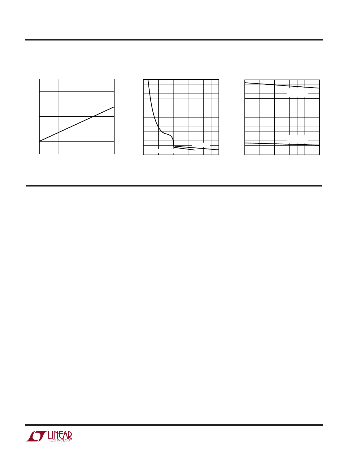
LTC1159
LOAD CURRENT (A)
0
–100
∆V
OUT
(mV)
–80
–60
–40
–20
0
20
0.5 1.0 1.5 2.0
LTC1159 • TPC03
2.5
FIGURE 1 CIRCUIT
V
IN
= 24V
LTC1159-3.3/LTC1159-5
LECTRICAL C CHARA TERIST
E
ICS
Note 6: The LTC1159C, LTC1159C-3.3, and LTC1159C-5 are not tested
and not quality assurance sampled at –40°C and 85°C. These
specifications are guaranteed by design and/or correlation. The LTC1159I,
LTC1159I-3.3 and LTC1159I-5 are guaranteed and tested over the –40°C
Note 7: The logic-level power MOSFETs shown in Figure 1 are rated for
V
= 30V. For operation at VIN > 30V, use standard threshold
DS(MAX)
MOSFETs with EXTV
Information.
to 85°C operating temperature range.
UW
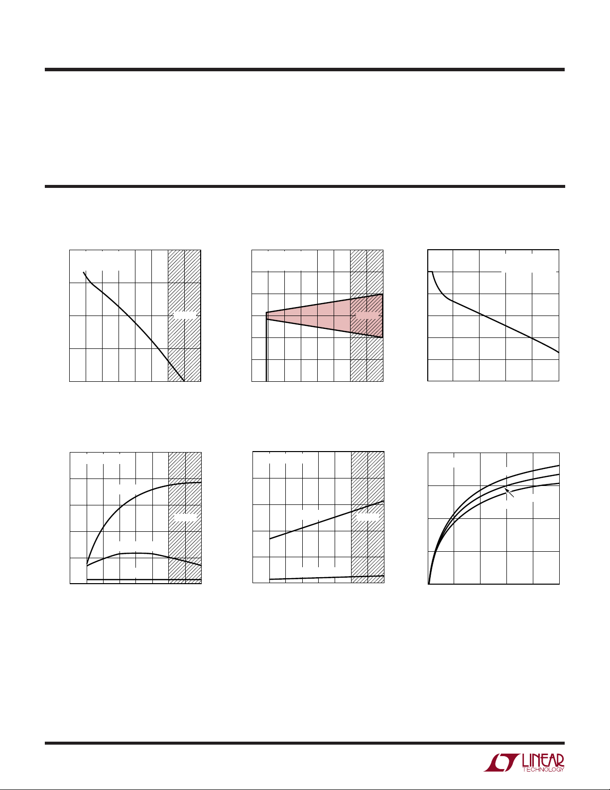
TYPICAL PERFOR A CE CHARACTERISTICS
Efficiency vs Input Voltage
100
FIGURE 1 CIRCUIT
I
= 1A
LOAD
95
90
EFFICIENCY (%)
85
80
0
5101520
INPUT VOLTAGE (V)
NOTE 6
25 30 35 40
LTC1159 • TPC01
Line Regulation
60
FIGURE 1 CIRCUIT
= 1A
I
LOAD
40
20
(mV)
0
OUT
∆V
–20
–40
–60
0
515
10 20
INPUT VOLTAGE (V)
30
25
NOTE 6
35
LT1159 • TPC02
powered from a 12V supply. See Applications
CC
Load Regulation
40
Operating Frequency
EXTVCC Pin Current
10
FIGURE 1 CIRCUIT
8
I
= 1A
LOAD
6
CURRENT (mA)
4
CC
I
= 100mA
EXTV
2
0
0
510
LOAD
I
= 0
LOAD
20
15 25 40
INPUT VOLTAGE (V)
NOTE 6
30 35
LTC1159 • TPC04
VIN Pin Current
500
FIGURE 1 CIRCUIT
400
300
200
SUPPLY CURRENT (µA)
100
0
0
510
INPUT VOLTAGE (V)
NORMAL
V
= 2V
SHDN2
20
15 25 40
NOTE 6
30 35
LTC1159 • TPC05
vs (VIN – V
2.0
V
= 5V
OUT
1.5
1.0
0.5
NORMALIZED FREQUENCY
0
0
5
(VIN – V
OUT
10
OUT
)
T = 0°C
T = 70°C
15
) VOLTAGE (V)
T = 25°C
20
25
LTC1159 • TPC06
4
Page 5
UW
TYPICAL PERFOR A CE CHARACTERISTICS
LTC1159
LTC1159-3.3/LTC1159- 5
EXTVCC Switch Drop Current Sense Threshold Voltage
600
500
400
(mV)
CC
300
– V
CC
200
EXTV
100
0
0
5101520
SWITCH CURRENT (mA)
LTC1159 • TPC07
U
UU
Off-Time vs V
80
70
60
50
40
30
OFF-TIME (µs)
20
10
0
0
OUT
LTC1159-3.3
1
2
OUTPUT VOLTAGE (V)
LTC1159-5
34
LTC1159 • TPC08
5
160
140
120
100
80
60
SENSE VOLTAGE (mV)
40
20
0
0
20
MAXIMUM
THRESHOLD
THRESHOLD
60 80
40
TEMPERATURE (°C)
PI FU CTIO S
VIN: Main Supply Input Pin.
SGND: Small-Signal Ground. Must be routed separately
from other grounds to the (–) terminal of C
OUT
.
PGND: Driver Power Grounds. Connect to source of Nchannel MOSFET and the (–) terminal of CIN.
VCC: Outputs of internal 4.5V linear regulator, EXTV
switch, and supply inputs for driver and control circuits.
The driver and control circuits are powered from the higher
of the 4.5V regulator or EXTVCC voltage. Must be closely
decoupled to power ground.
SENSE+: The (+) Input for the Current Comparator. A builtin offset between the SENSE+ and SENSE– pins, in conjunction with R
, sets the current trip threshold.
SENSE
N-Gate: High Current Drive for the Bottom N-Channel
MOSFET. The N-Gate pin swings from ground to VCC.
P-Gate: Level-Shifted Gate Drive Signal for the Top
CC
P-Channel MOSFET. The voltage swing at the P-gate pin is
from VIN to VIN – VCC.
P-Drive: High Current Gate Drive for the Top P-Channel
MOSFET. The P-drive pin(s) swing(s) from VCC to ground.
MINIMUM
100
LTC1159 • TPC09
CT: External capacitor CT from this pin to ground sets the
operating frequency. (The frequency is also dependent on
the ratio V
OUT/VIN
.)
ITH: Gain Amplifier Decoupling Point. The current comparator threshold increases with the I
pin voltage.
TH
VFB: For the LTC1159 adjustable version, the VFB pin
receives the feedback voltage from an external resistive
divider used to set the output voltage.
SENSE–: Connects to internal resistive divider which sets
the output voltage in fixed output versions. The SENSE– pin
is also the (–) input of the current comparator.
CAP: Charge Compensation Pin. A capacitor to VCC pro-
vides charge required by the P-gate level-shift capacitor
during supply transitions.
pacitor must be larger than the gate drive capacitor
SHDN1: This pin shuts down the control circuitry only (V
The charge compensation ca-
.
CC
is not affected). Taking SHDN1 pin high turns off the
control circuitry and holds both MOSFETs off. This pin
must be at ground potential for normal operation.
SHDN2: Master Shutdown Pin. Taking SHDN2 high shuts
down VCC and all control circuitry.
5
Page 6
LTC1159
LTC1159-3.3/LTC1159-5
U
U
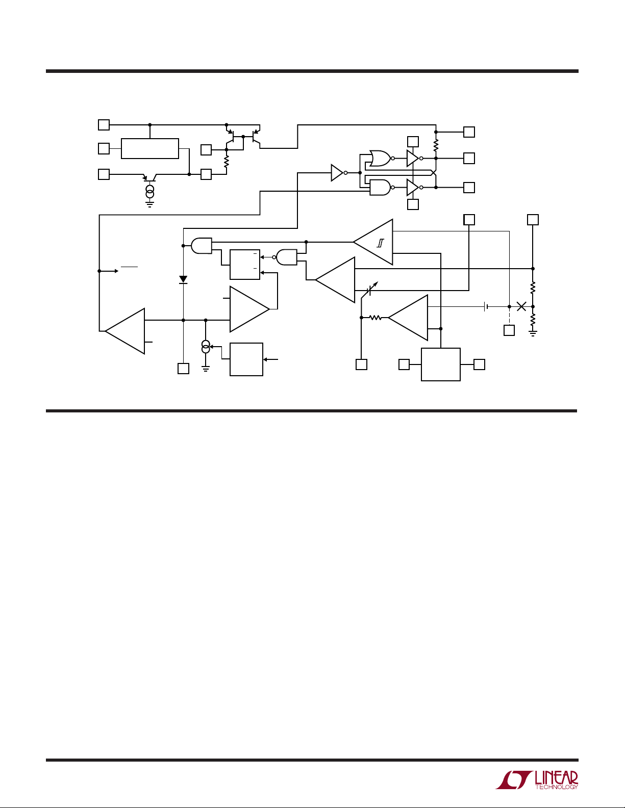
W
FU CTIO AL DIAGRA
V
IN
SHDN2
EXTV
LOW DROPOUT
4.5V REGULATOR
CC
LOW DROP SWITCH
SLEEP
+
S
V
–
TH2
CAP
V
CC
V
C
T
Internal divider broken at VFB for adjustable versions.
550k
PGND
–
V
+
25mV TO 150mV
13k
SGND
TH
TH1
Q
–
T
+
OFF-TIME
CONTROL
R
S
–
SENSE
–
C
+
I
V
CC
G
550k
–
+
1.25V
REFERENCE
SENSE
P-GATE
P-DRIVE
N-GATE
+
V
OS
SHDN1
–
SENSE
100k
LTC1159 • FD
V
FB
U
OPERATIO
The LTC1159 uses a current mode, constant off-time
architecture to synchronously switch an external pair of
complementary power MOSFETs. Operating frequency is
set by an external capacitor at the CT pin.
The output voltage is sensed either by an internal voltage
divider connected to the SENSE– pin (LTC1159-3.3 and
LTC1159-5) or an external divider returned to the VFB pin
(LTC1159). A voltage comparator V, and a gain block G,
compare the divided output voltage with a reference voltage of 1.25V. To optimize efficiency, the LTC1159 automatically switches between two modes of operation, burst
and continuous.
A low dropout 4.5V regulator provides the operating voltage VCC for the MOSFET drivers and control circuitry during
start-up. During normal operation, the LTC1159 family
powers the drivers and control from the output via the
EXTVCC pin to improve efficiency. The N-GATE pin is
referenced to ground and drives the N-channel MOSFET
gate directly. The P-channel gate drive must be referenced
to the main supply input VIN, which is accomplished by
(Refer to Functional Diagram)
level-shifting the P-drive signal via an internal 550k resistor
and external capacitor.
During the switch “ON” cycle in continuous mode, current
comparator C monitors the voltage between the SENSE
+
and SENSE– pins connected across an external shunt in
series with the inductor. When the voltage across the shunt
reaches its threshold value, the P-gate output is switched
to VIN, turning off the P-channel MOSFET. The timing
capacitor CT is now allowed to discharge at a rate determined by the off-time controller. The discharge current is
made proportional to the output voltage to model the
inductor current, which decays at a rate which is also
proportional to the output voltage. While the timing
capacitor is discharging, the N-gate output is high, turning
on the N-channel MOSFET.
When the voltage on CT has discharged past V
, compara-
TH1
tor T trips, setting the flip-flop. This causes the N-gate output
to go low (turning off the N-channel MOSFET) and the Pgate output to also go low (turning the P-channel MOSFET
back on). The cycle then repeats. As the load current
6
Page 7

OPERATIO
LTC1159
LTC1159-3.3/LTC1159- 5
U
(Refer to Functional Diagram)
increases, the output voltage decreases slightly. This causes
the output of the gain stage to increase the current comparator threshold, thus tracking the load current.
The sequence of events for Burst Mode operation is very
similar to continuous operation with the cycle interrupted
by the voltage comparator. When the output voltage is at or
above the desired regulated value, the P-channel MOSFET
is held off by comparator V and the timing capacitor continues to discharge below V
discharges past V
the internal SLEEP line to go low and the N-channel MOSFET
to turn off.
The circuit now enters sleep mode with both power
MOSFETs turned off. In sleep mode, much of the circuitry
, voltage comparator S trips, causing
TH2
. When the timing capacitor
TH1
WUUU
APPLICATIO S I FOR ATIO
The LTC1159 Compared to the LTC1148/LTC1149
Families
The LTC1159 family is closest in operation to the LTC1149
and shares much of the applications information. In addition to reduced quiescent and shutdown currents, the
LTC1159 adds an internal switch which allows the driver
and control sections to be powered from an external
source for higher efficiency. This change affects Power
MOSFET Selection, EXTVCC Pin Connection, Important
Information About LTC1159 Adjustable Applications, and
Efficiency Considerations found in this section.
The basic LTC1159 application circuit shown in Figure 1
is limited to a maximum input voltage of 30V due to
MOSFET breakdown. If the application does not require
greater than 18V operation, then the LTC1148 or
LTC1148HV should be used. For higher input voltages
where quiescent and shutdown current are not critical, the
LTC1149 may be a better choice since it is set up to drive
standard threshold MOSFETs.
R
R
LTC1159 current comparator has a threshold range that
extends from a minimum of 0.025V/R
Selection for Output Current
SENSE
is chosen based on the required output current. The
SENSE
to a maximum
SENSE
is turned off, dropping the supply current from several
milliamps (with the MOSFETs switching) to 300µA. When
the output capacitor has discharged by the amount of
hysteresis in comparator V, the P-channel MOSFET is
again turned on and this process repeats. To avoid the
operation of the current loop interfering with Burst Mode
operation, a built-in offset is incorporated in the gain stage.
To prevent both the external MOSFETs from being turned
on at the same time, feedback is incorporated to sense the
state of the driver output pins. Before the N-gate output can
go high, the P-drive output must also be high. Likewise, the
P-drive output is prevented from going low when the
N-gate output is high.
of 0.15V/R
the peak of the inductor ripple current, yielding a maximum
output current I
peak-to-peak ripple current.
tion, I
RIPPLE(P-P)
. The current comparator threshold sets
SENSE
equal to the peak value less half the
MAX
For proper Burst Mode opera-
must be less than or equal to the minimum
current comparator threshold.
Since efficiency generally increases with ripple current,
the maximum allowable ripple current is assumed, i.e.,
I
RIPPLE(P-P)
Operating Frequency). Solving for R
a margin for variations in the LTC1159 and external
component values yields:
R
SENSE
A graph for selecting R
current is given in Figure 2. The LTC1159 series works well
with values of R
The load current below which Burst Mode operation commences, I
both track I
I
SC(PK)
= 0.025V/R
100
= mΩ
I
MAX
from 0.02Ω to 0.2Ω.
SENSE
, and the peak short-circuit current, I
BURST
. Once R
MAX
can be predicted from the following equations:
(see CT and L Selection for
SENSE
SENSE
versus maximum output
SENSE
has been chosen, I
SENSE
and allowing
SC(PK)
and
BURST
,
7
Page 8

LTC1159
LTC1159-3.3/LTC1159-5
WUUU
APPLICATIO S I FOR ATIO
0.20
0.18
0.16
0.14
0.12
(Ω)
0.10
SENSE
R
0.08
0.06
0.04
0.02
0
1
0
MAXIMUM OUTPUT CURRENT (A)
2
3
4
5
LTC1159 • F02
1400
1200
1000
800
600
CAPACITANCE (pF)
T
400
C
200
0
50
0
VIN = 48V
150
100
FREQUENCY (kHz)
V
OUT
= 24V
V
IN
VIN = 12V
200
= 5V
250
LTC1159 • F03
Figure 2. R
I
BURST
I
SC(PK)
≈
=
15mV
R
SENSE
150mV
R
SENSE
The LTC1159 automatically extends t
vs Maximum Output Current
SENSE
during a short
OFF
circuit to allow sufficient time for the inductor current to
decay between switch cycles. The resulting ripple current
causes the average short-circuit current I
reduced to approximately I
MAX
.
SC(AVG)
to be
L and CT Selection for Operating Frequency
The LTC1159 uses a constant off-time architecture with
t
determined by an external timing capacitor CT. The
OFF
value of CT is calculated from the desired continuous mode
operating frequency, f:
CT =
7.8 • 10
f
–5
1 –
)
V
OUT
V
IN
)
A graph for selecting CT versus frequency including the
effects of input voltage is given in Figure 3.
As the operating frequency is increased the gate charge
losses will be higher, reducing efficiency (see Efficiency
Considerations). The complete expression for operating
frequency is given by:
f =
t
OFF
1
1 –
)
V
OUT
V
IN
)
Figure 3. Timing Capacitor Selection
where t
= 1.3 • 104 • C
OFF
T
Once the frequency has been set by CT, the inductor L
must be chosen to provide no more than 0.025V/R
SENSE
of peak-to-peak inductor ripple current. This results in a
minimum required inductor value of:
L
= 5.1 • 105 • R
MIN
SENSE
• CT • V
REG
As the inductor value is increased from the minimum value,
the ESR requirements for the output capacitor are eased at
the expense of efficiency. If too small an inductor is used,
the LTC1159 may not enter Burst Mode operation and
efficiency will be severely degraded at low currents.
Inductor Core Selection
Once the minimum value for L is known, the type of
inductor must be selected. High efficiency converters
generally cannot afford the core loss found in low cost
powdered iron cores, forcing the use of more expensive
ferrite, molypermalloy or Kool Mµ® cores. Actual core loss
is independent of core size for a fixed inductor value, but
it is very dependent on the inductance selected. As induc
tance increases, core losses go down but copper (I2R)
losses will increase.
Ferrite designs have very low core loss, so design goals can
concentrate on copper loss and preventing saturation.
Ferrite core material saturates “hard,” which means that
inductance collapses abruptly when the peak design current is exceeded. This results in an abrupt increase in
Kool Mµ is a registered trademark of Magnetics, Inc.
8
Page 9

V
V
WUUU
APPLICATIO S I FOR ATIO
LTC1159
LTC1159-3.3/LTC1159- 5
inductor ripple current and consequent output voltage
ripple which can cause Burst Mode operation to be falsely
triggered in the LTC1159. Do not allow the core to saturate!
Molypermalloy (from Magnetics, Inc.) is a low loss core
material for toroids, but it is more expensive than ferrite.
A reasonable compromise from the same manufacturer is
Kool Mµ. Toroids are very space efficient, especially when
you can use several layers of wire. Because they generally
lack a bobbin, mounting is more difficult. However, new
surface mount designs available from Coiltronics do not
increase the height significantly.
Power MOSFET Selection
Two external power MOSFETs must be selected for use
with the LTC1159: a P-channel MOSFET for the main
switch and an N-channel MOSFET for the synchronous
switch.
The peak-to-peak drive levels are set by the VCC voltage on
the LTC1159. This voltage is typically 4.5V during start-up
and 5V to 7V during normal operation (see EXTVCC Pin
Connection). Consequently,
logic-level threshold
MOSFETs must be used in most LTC1159 family applications
. The only exception is applications in which EXTV
CC
is powered from an external supply greater than 8V, in
which standard threshold MOSFETs (V
used. Pay close attention to the BV
DSS
< 4V) may be
GS(TH)
specification for the
MOSFETs as well; many of the logic-level MOSFETs are
limited to 30V.
Selection criteria for the power MOSFETs include the “ON”
resistance R
, reverse transfer capacitance C
DS(ON)
RSS
,
input voltage and maximum output current. When the
LTC1159 is operating in continuous mode, the duty cycle
for the P-channel MOSFET is given by:
P-Ch Duty Cycle =
N-Ch Duty Cycle =
OUT
V
IN
V
IN – VOUT
V
IN
The MOSFET dissipations at maximum output current are
given by:
P-Ch PD =
N-Ch PD =
where ∂ is the temperature dependency of R
OUT
V
IN
k(V
)2 (I
IN
V
IN – VOUT
V
IN
(I
MAX
MAX
(I
)2 (1 + ∂P) R
) (C
MAX
) (f)
RSS
)2 (1 + ∂N) R
DS(ON)
DS(ON)
+
DS(ON)
and k
is a constant inversely related to the gate drive current.
Both MOSFETs have I2R losses while the P-channel
equation includes an additional term for transition losses,
which are highest at high input voltages. For VIN < 20V the
high current efficiency generally improves with larger
MOSFETs, while for VIN > 20V the transition losses rapidly
increase to the point that the use of a higher R
device with lower C
actually provides higher effi-
RSS
DS(ON)
ciency. The N-channel MOSFET losses are the greatest at
high input voltage or during a short circuit when the
N-channel duty cycle is nearly 100%.
The term (1 + ∂) is generally given for a MOSFET in the form
of a normalized R
vs Temperature curve, but
DS(ON)
∂ = 0.007/°C can be used as an approximation for low
voltage MOSFETs. C
is usually specified in the MOSFET
RSS
electrical characteristics. The constant k = 5 can be used for
the LTC1159 to estimate the relative contributions of the
two terms in the P-channel dissipation equation.
The Schottky diode D1 shown in Figure 1 only conducts
during the dead time between the conduction of the two
power MOSFETs. D1 prevents the body diode of the
N-channel MOSFET from turning on and storing charge
during the dead time, which could cost as much as 1% in
efficiency (although there are no other harmful effects if
D1 is omitted). Therefore, D1 should be selected for a
forward voltage of less than 0.6V when conducting I
MAX
.
9
Page 10

LTC1159
LTC1159-3.3/LTC1159-5
WUUU
APPLICATIO S I FOR ATIO
CIN and C
Selection
OUT
In continuous mode, the source current of the P-channel
MOSFET is a square wave of duty cycle V
OUT/VIN
.
To prevent large voltage transients, a low ESR input
capacitor sized for the
maximum RMS current must be
used. The maximum RMS capacitor current is given by:
OUT
1/2
)]
, where
CIN Required I
RMS
≈
MAX
OUT(VIN – VOUT
V
IN
[V
I
This formula has a maximum at VIN = 2V
I
RMS
= I
/2. This simple worst-case condition is com-
MAX
monly used for design because even significant deviations
do not offer much relief. Note that capacitor manufacturer’s
ripple current ratings are often based on only 2000 hours
of life. This makes it advisable to further derate the
capacitor, or to choose a capacitor rated at a higher
temperature than required. Several capacitors may be
paralleled to meet size or height requirements in the
design. An additional 0.1µF ceramic capacitor may also be
required on VIN for high frequency decoupling.
The selection of C
series resistance (ESR). The ESR of C
twice the value of R
is driven by the required effective
OUT
must be less than
OUT
for proper operation of the
SENSE
LTC1159:
C
Required ESR < 2R
OUT
SENSE
Optimum efficiency is obtained by making the ESR equal to
R
. Manufacturers such as Nichicon, Chemicon, and
SENSE
Sprague should be considered for high performance capacitors. The OS-CON semiconductor dielectric capacitor
available from Sanyo has the lowest ESR for its size at a
somewhat higher price. Once the ESR requirement for
C
has been met, the RMS current rating generally far
OUT
exceeds the I
RIPPLE(P-P)
requirement.
In surface mount applications, multiple capacitors may
have to be paralleled to meet the capacitance, ESR or RMS
current handling requirements of the application. Aluminum electrolytic and dry tantalum capacitors are both
available in surface mount configurations. In the case of
tantalum, it is critical that the capacitors are surge tested
for use in switching power supplies. An excellent choice is
the AVX TPS series of surface mount tantalums, available
in case heights ranging from 2mm to 4mm. For example,
if 200µF/10V is called for in an application requiring 3mm
height, two AVX 100µF/10V (P/N TPSD107K010) could be
used. Consult the manufacturer for other specific recommendations.
At low supply voltages, a minimum value of C
OUT
is
suggested to prevent an abnormal low frequency operating
mode (see Figure 4). When C
is too small, the output
OUT
ripple at low frequencies will be large enough to trip the
voltage comparator. This causes the Burst Mode operation
to be activated when the LTC1159 would normally be in
continuous operation. The effect is most pronounced with
low values of R
and can be improved by operating at
SENSE
higher frequencies with lower values of L. The output
remains in regulation at all times.
1000
800
600
(µF)
OUT
C
400
R
SENSE
200
0
0
Figure 4. Minimum Suggested C
L = 50µH
= 0.05Ω
1
(VIN – V
L = 50µH
R
SENSE
L = 25µH
R
SENSE
2
) VOLTAGE (V)
OUT
= 0.02Ω
= 0.02Ω
3
4
LTC1159 • TPC04
OUT
5
Load Transient Response
Switching regulators take several cycles to respond to a
step in DC (resistive) load current. When a load step
occurs, V
where ESR is the effective series resistance of C
also begins to charge or discharge C
loop adapts to the current change and returns V
steady-state value. During this recovery time V
shifts by an amount equal to ∆I
OUT
OUT
• ESR,
LOAD
. ∆I
OUT
LOAD
until the regulator
to its
OUT
can be
OUT
monitored for overshoot or ringing which would indicate a
stability problem. The ITH external components shown in
the Figure 1 circuit will provide adequate compensation for
most applications.
A second, more severe transient is caused by switching in
loads with large (>1µF) supply bypass capacitors. The
10
Page 11

WUUU
APPLICATIO S I FOR ATIO
LTC1159
LTC1159-3.3/LTC1159- 5
discharged bypass capacitors are effectively put in parallel
with C
, causing a rapid drop in V
OUT
. No regulator can
OUT
deliver enough current to prevent this problem if the load
switch resistance is low and it is driven quickly. The only
solution is to limit the rise time of the switch drive so that
the load rise time is limited to approximately 25 • C
LOAD
.
Thus a 10µF capacitor would require a 250µs rise time,
limiting the charging current to about 200mA.
Line Transient Response
The LTC1159 has better than 60dB line rejection and is
generally impervious to large positive or negative line
voltage transients. However, one rarely occurring condition can cause the output voltage to overshoot if the proper
precautions are not observed. This condition is a negative
VIN transition of several volts followed within 100µs by a
positive transition of greater than 0.5V/µs slew rate.
The reason this condition rarely occurs is because it takes
tens of amps to slew the regulator input capacitor at this
rate! The solution is to add a diode between the cap and V
IN
pins of the LTC1159 as shown in several of the typical
application circuits. If you think your system could have
this problem, add the diode. Note that in surface mount
applications it can be combined with the P-gate diode by
using a low cost common cathode dual diode.
EXTVCC Pin Connection
The LTC1159 contains an internal PNP switch connected
between the EXTVCC and VCC pins. The switch closes and
supplies the VCC power whenever the EXTVCC pin is higher
in voltage than the 4.5V internal regulator. This allows the
V
IN
V
IN
P-DRIVE
LTC1159-3.3
P-GATE
N-GATE
P-GND
EXTV
+
C
P-CH
N-CH
CC
BAT85
IN
R
SENSE
C
1µF
OUT
+
21
4
+
LTC1159 • F05a
V
OUT
L
1:1
•
•
3
MOSFET driver and control power to be derived from the
output during normal operation and from the internal
regulator when the output is out of regulation (start-up,
short circuit).
Significant efficiency gains can be realized by powering V
CC
from the output, since the VIN current resulting from the
driver and control currents will be scaled by a factor of
(Duty Cycle)/(Efficiency). For 5V regulators this simply
means connecting the EXTVCC pin directly to V
OUT
. However, for 3.3V and other low voltage regulators, additional
circuitry is required to derive VCC power from the output.
The following list summarizes the four possible connections for EXTVCC:
1. EXTVCC Left Open. This will cause VCC to be powered
only from the internal 4.5V regulator resulting in reduced
MOSFET gate drive levels and an efficiency penalty of up to
10% at high input voltages.
2. EXTVCC Connected Directly to V
. This is the normal
OUT
connection for a 5V regulator and provides the highest
efficiency.
3. EXTVCC Connected to an Output-Derived Boost Network. For 3.3V and other low voltage regulators, efficiency
gains can still be realized by connecting EXTVCC to an
output-derived voltage which has been boosted to greater
than 4.5V. This can be done either with the inductive boost
winding shown in Figure 5a or the capacitive charge pump
shown in Figure 5b. The charge pump has the advantage of
simple magnetics and generally provides the highest efficiency at the expense of a slightly higher parts count.
V
IN
+
C
BAT85
IN
VN2222LL
L
0.22µF
LTC1159 • F05b
R
SENSE
BAT85
BAT85
V
OUT
+
C
OUT
V
IN
P-DRIVE
LTC1159-3.3
P-GATE
N-GATE
P-GND
EXTV
P-CH
N-CH
CC
+
1µF
Figure 5a. Inductive Boost Circuit for EXTV
CC
Figure 5b. Capacitive Charge Pump for EXTV
CC
11
Page 12

LTC1159
LTC1159-3.3/LTC1159-5
WUUU
APPLICATIO S I FOR ATIO
4. EXTVCC Connected to an External Supply. If an external
supply is available in the 5V to 12V range, it may be used
to power EXTVCC providing it is compatible with the
MOSFET gate drive requirements. There are no restrictions
on the EXTVCC voltage relative to VIN. EXTVCC may be
higher than VIN providing EXTV
does not exceed the 15V
CC
absolute maximum rating.
When driving standard threshold MOSFETs, the external supply must always be present during operation to
prevent MOSFET failure due to insufficient gate drive
. The
LTC1149 family should also be considered for applications
which require the use of standard threshold MOSFETs.
Important Information About LTC1159 Adjustable
Applications
When an output voltage other than 3.3V or 5V is required,
the LTC1159 adjustable version is used with an external
resistive divider from V
to the VFB pin (Figure 6). The
OUT
regulated voltage is determined by:
V
= 1.25V
OUT
1 +
)
R2
R1
)
The VFB pin is extremely sensitive to pickup from the
inductor switching node
. Care should be taken to isolate
the feedback network from the inductor, and the 100pF
capacitor should be connected between the VFB and SGND
pins next to the package.
In LTC1159N and LTC1159S applications with V
OUT
>
5.5V, the VCC pin may self-power through the SENSE pins
when SHDN2 is taken high, preventing shutdown. In these
applications, a pull-down must be added to the SENSE– pin
as shown in Figure 6. This pull-down effectively takes the
place of the SHDN1 pin, ensuring complete shutdown.
Note: For versions in which both the SHDN1 and SHDN2
pins are available (LTC1159G and all fixed output versions), the two pins are simply connected to each other and
driven together to guarantee complete shutdown.
The Figure 6 circuit cannot be used to regulate a V
OUT
which
is greater than the maximum voltage allowed on the
LTC1159 SENSE pins (13V). In applications with V
13V, R
must be moved to the ground side of the
SENSE
OUT
>
output capacitor and load. This operates the current sense
comparator at 0V common mode, increasing the off-time
approximately 40% and requiring the use of a smaller
timing capacitor CT.
Inverting Regular Applications
The LTC1159 can also be used to obtain negative output
voltages from positive inputs. In these inverting applications, the current sense resistor connects to ground while
the LTC1159 and N-channel MOSFET connections, which
would normally go to ground, instead ride on the negative
output. This allows the negative output voltage to be set by
V
IN
12
+
1µF
3300pF
1k
0V = NORMAL
>3V = SHUTDOWN
+
Si4401DY
Si4840DY
=
V
OUT
VALUES SHOWN FOR V
0.15µF
C
T
390pF
CAP
V
CC
V
CC
I
TH
C
T
SHDN2
V
IN
LTC1159
P-GATE
P-DRIVE
N-GATE
PGND
EXTV
V
SGND
SENSE
SENSE
1N4148
0.1µF
5M
CC
FB
+
–
100pF
0.01µF
VN2222LL
100Ω
100Ω
Figure 6. High Efficiency Adjustable Regulator with 5.5V < V
100µF
50V
100µH
1N5819
R2
1 +
()
R1
1.25
3
OUT
OUT
R
SENSE
0.039Ω
LTC1159 • F06
= 12V/2.5A
< 13V
21
4
R2
215k
R1
24.9k
V
OUT
+
150µF
16V
OS-CON
Page 13

WUUU
APPLICATIO S I FOR ATIO
LTC1159
LTC1159-3.3/LTC1159- 5
the same process as in conventional applications, using
either the internal divider (LTC1159-3.3, LTC1159-5) or an
external divider with the adjustable version.
Figure 15 in the Typical Applications shows a synchronous
12V to –12V converter that can supply up to 1A with better
than 85% efficiency. By grounding the EXTVCC pin in the
Figure 15 circuit, the entire 12V output voltage is placed
across the driver and control circuits since the LTC1159
ground pins are at –12V. During start-up or short-circuit
conditions, operating power is supplied by the internal
4.5V regulator. The shutdown signal is level-shifted to the
negative output rail by Q3, and Q4 ensures that Q1 and Q2
remain off during the entire shutdown sequence.
Efficiency Considerations
The percent efficiency of a switching regulator is equal to
the output power divided by the input power times 100%.
It is often useful to analyze individual losses to determine
what is limiting the efficiency and which change would
produce the most improvement. Percent efficiency can be
expressed as:
%Efficiency = 100 – (L1 + L2 + L3 + ...)
where L1, L2, etc., are the individual losses as a percentage
of input power.
Although all dissipative elements in the circuit produce
losses, four main sources usually account for most of the
losses in LTC1159 circuits: 1) LTC1159 VIN current, 2)
LTC1159 VCC current, 3) I2R losses and 4) P-channel
transition losses.
1. LTC1159 VIN current is the DC supply current given in
the electrical characteristics which excludes MOSFET driver
and control currents. VIN current results in a small (<1%)
loss which increases with VIN.
2. LTC1159 VCC current is the sum of the MOSFET driver
and control circuit currents. The MOSFET driver current
results from switching the gate capacitance of the power
MOSFETs. Each time a MOSFET gate is switched from low
to high to low again, a packet of charge dQ moves from V
to ground. The resulting dQ/dt is a current out of VCC which
is typically much larger than the control circuit current. In
continuous mode, I
are the gate charges of the two MOSFETs.
GATECHG
≈ f (QP + QN), where QP and Q
CC
N
By powering EXTVCC from an output-derived source, the
additional VIN current resulting from the driver and control
currents will be scaled by a factor of (Duty Cycle)/(Efficiency). For example in a 20V to 5V application, 10mA of
VCC current results in approximately 3mA of VIN current.
This reduces the mid-current loss from 10% or more (if the
driver was powered directly from VIN) to only a few percent.
3. I2R losses are easily predicted from the DC resistances
of the MOSFET, inductor and current shunt. In continuous
mode all of the output current flows through L and
R
N-channel MOSFETs. If the two MOSFETs have approximately the same R
MOSFET can simply be summed with the resistances of L
and R
R
the total resistance is 0.3Ω. This results in losses ranging
from 3% to 12% as the output current increases from
0.5A to 2A. I2R losses cause the efficiency to roll-off at
high output currents.
4. Transition losses apply only to the P-channel MOSFET,
and only when operating at high input voltages (typically
20V or greater). Transition losses can be estimated from:
Other losses including CIN and C
Schottky conduction losses during dead time, and inductor
core losses, generally account for less than 2% total
additional loss.
Auxiliary Windings—Suppressing Burst Mode
Operation
The LTC1159 synchronous switch removes the normal
limitation that power must be drawn from the inductor
primary winding in order to extract power from auxiliary
windings. With synchronous switching, auxiliary outputs may be loaded without regard to the primary output
load, providing that the loop remains in continuous
mode operation.
Burst Mode operation can be suppressed at low output
currents with a simple external network that cancels the
0.025V minimum current comparator threshold. This technique is also useful for eliminating audible noise from
, but is “chopped” between the P-channel and
SENSE
, then the resistance of one
DS(ON)
to obtain I2R losses. For example, if each
SENSE
= 0.1Ω, RL = 0.15Ω, and R
DS(ON)
Transition Loss ≈ 5(VIN)2(I
)(C
MAX
ESR dissipative losses,
OUT
= 0.05Ω, then
SENSE
)(f)
RSS
13
Page 14

LTC1159
LTC1159-3.3/LTC1159-5
WUUU
APPLICATIO S I FOR ATIO
certain types of inductors in high current (I
OUT
> 5A)
applications when they are lightly loaded.
An external offset is put in series with the SENSE– pin to
subtract from the built-in 0.025V offset. An example of this
technique is shown in Figure 7. Two 100Ω resistors are
inserted in series with the leads from the sense resistor.
With the addition of R3, a current is generated through R1
causing an offset of:
V
OFFSET
LTC1159
= V
SENSE
SENSE
OUT
9
+
8
–
R1
)
R1 + R3
1000pF
)
R
3
SENSE
LTC1159 • F07
21
4
+
C
OUT
L
R2
100Ω
R1
100Ω
R3
If V
> 0.025V, the minimum threshold will be
OFFSET
cancelled and Burst Mode operation is prevented from
occurring. Since V
is constant, the maximum load
OFFSET
current is also decreased by the same offset. Thus, to get
back to the same I
, the value of the sense resistor must
MAX
be reduced:
R
SENSE
75
≈ mΩ
I
MAX
To prevent noise spikes from erroneously tripping the
current comparator, a 1000pF capacitor is needed across
the SENSE– and SENSE+ pins.
Board Layout Checklist
When laying out the printed circuit board, the following
checklist should be used to ensure proper operation of the
LTC1159. These items are also illustrated graphically in
the layout diagram of Figure 8. Check the following in your
layout:
Figure 7. Suppressing Burst Mode Operation
BOLD LINES INDICATE HIGH CURRENT PATHS
1N4148
0.15µF
1µF
+
1
P-GATE
2
V
IN
3
4
5
6
7
8
V
CC
P-DRIVE
V
CC
C
T
I
TH
SENSE
–
0.1 µF
3300pFC
T
1k
CAP
SHDN2
EXTV
N-GATE
PGND
SGND
V
(SHDN1)
SENSE
1000pF
CC
FB
+
16
15
14
13
12
11
10
9
SHUTDOWN
100pF
P-CHANNEL
5V EXTV
CONNECTION
R1
R2
+
C
IN
+
D1
N-CHANNEL
V
IN
–
L
CC
OUTPUT DIVIDER
REQUIRED WITH
ADJUSTABLE
VERSION ONLY
–
3
C
OUT
+
1
V
OUT
R
SENSE
2
4
+
14
LTC1159 • F08
Figure 8. LTC1159 Layout Diagram (N and S Packages)
Page 15

WUUU
APPLICATIO S I FOR ATIO
LTC1159
LTC1159-3.3/LTC1159- 5
1) Are the signal and power grounds segregated? The
LTC1159 signal ground must connect separately to the
(–) plate of C
. The other ground pin(s) should return to
OUT
the source of the N-channel MOSFET, anode of the Schottky diode and (–) plate of CIN, which should have as short
lead lengths as possible.
2) Does the LTC1159 SENSE– pin connect to a point close
to R
and the (+) plate of C
SENSE
? In adjustable applica-
OUT
tions, the resistive divider R1, R2 must be connected
between the (+) plate of C
3
) Are the SENSE– and SENSE+ leads routed together
and signal ground.
OUT
with minimum PC trace spacing? The differential
decoupling capacitor between the two SENSE pins should
be as close as possible to the LTC1159. Up to 100Ω may
be placed in series with each sense lead to help decouple
the SENSE pins. However, when these resistors are used,
the capacitor should be no larger than 1000pF.
4) Does the (+) plate of CIN connect to the source of the
P-channel MOSFET as closely as possible? An additional
0.1µF ceramic capacitor between VIN and power ground
may be required in some applications.
5) Is the VCC decoupling capacitor connected closely between the VCC pins of the LTC1159 and power ground?
This capacitor carries the MOSFET driver peak currents.
6) In adjustable versions, the feedback pin is very sensitive
to pickup from the switch node. Care must be taken to
isolate VFB from possible capacitive coupling of the inductor switch signal.
7) Is the SHDN1 pin actively pulled to ground during
normal operation? SHDN1 is a high impedance pin and
must not be allowed to float.
Troubleshooting Hints
Since efficiency is critical to LTC1159 applications it is very
important to verify that the circuit is functioning correctly
in both continuous and Burst Mode operation. The waveform to monitor is the voltage on the CT pin .
In continuous mode (I
a sawtooth with a 0.9V
> I
LOAD
swing. This voltage should never
P-P
) the voltage should be
BURST
dip below 2V as shown in Figure 9a. When the load current
is low (I
LOAD
< I
), Burst Mode operation should occur
BURST
with the CT waveform periodically falling to ground as
shown in Figure 9b.
If the CT pin is observed falling to ground at high output
currents, it indicates poor decoupling or improper grounding. Refer to the Board Layout Checklist.
3.3V
(a) CONTINUOUS MODE OPERATION
(b) Burst Mode OPERATION
Figure 9. CT Pin 6 Waveforms
0V
3.3V
0V
LTC1159 • F09
15
Page 16

LTC1159
LTC1159-3.3/LTC1159-5
U
TYPICAL APPLICATIO S
1N4148
1N4148
V
IN
8V TO 20V5V
+
IRF7205
47µF
25V × 2
OS-CON
1µF
WIMA
1
0.15µF
0.1µF
+
3.3µF
1000pF
0.047µF
2k 10k
2
3
4
5
6
7
8
*MAGNETICS 77120-A7 CORE, 16T 18GA. WIRE
**KRL SL-1-R020J
Figure 10. High Efficiency 8V to 20V Input 2.5/5A Output Regulator
1N4148 1N4148
1
P-GATE
0.15µF
0.1µF
+
1µF
270pF
3300pF
1k
2
V
IN
3
V
CC
4
P-DRIVE
LTC1159-3.3
5
V
CC
6
C
T
7
I
TH
8
–
SENSE
*COILTRONICS CTX20-4
**KRL SL-1/2-R040J
P-GATE
V
IN
V
CC
P-DRIVE
V
CC
C
T
I
TH
SENSE
CAP
SHDN2
EXTV
N-GATE
PGND
SGND
SHDN1
SENSE
LTC1159
–
16
15
14
CC
13
12
11
10
9
+
CAP
SHDN2
EXTV
N-GATE
PGND
SGND
V
SENSE
16
15
14
CC
13
12
11
10
FB
9
+
V
IN
4V TO 20V
SHUTDOWN
100pF
1000pF
+
Si9435DY
Si9410DY MBRS130LT3
SHUTDOWN
0.01µF
47µF
25V
OS-CON
IRF7201IRF7201 MBRS330
10k
1%
100Ω
100Ω
10k
1%
0.1µF
BAT85
L*
15µH
L*
20µH
VN2222LL
0.22µF
**
R
SENSE
0.02Ω
3
BAT85
BAT85
3
R
21
4
LTC1159 • F10
SENSE
0.04Ω
V
OUT
2.5V/5A
+
330µF
6.3V × 3
AVX
**
21
V
OUT
3.3V/2.5A
4
+
330µF
6.3V × 2
AVX
+
1µF
LTC1159 • F11
16
Figure 11. 5:1 Input Range (4V to 20V) High Efficiency 3.3V/2.5A Regulator
Page 17

TYPICAL APPLICATIO S
U
12V
LTC1159
LTC1159-3.3/LTC1159- 5
V
IN
15V TO 40V
+
MPSA06
MPSA56
10µF
0.33µF
0.1µF
750pF
1N4148 1N4148
1
P-GATE
0.15µF
0.047µF
470Ω
2
V
IN
3
V
CC
4
P-DRIVE
LTC1159-5
5
V
CC
6
C
T
7
I
TH
8
–
SENSE
*HURRICANE LAB HL-KK122T/BB
**DALE LVR-3-0.01
CAP
SHDN2
EXTV
N-GATE
PGND
SGND
SHDN1
SENSE
16
15
14
CC
13
12
11
10
9
+
1N4148
MPSA56
SHUTDOWN
1000pF
18k
SMP40P06
HEAT SINK
MTP75N05HD
100Ω
100Ω
L*
22µH
MBR350
Figure 12. High Current, High Efficiency 15V to 40V Input 5V/10A Output Regulator
+
3
R
1200µF
50V × 2
LXF
SENSE
0.01Ω
**
21
4
LTC1159 • F12
1µF
WIMA
V
OUT
5V/10A
220µF
+
10V × 3
OS-CON
1N4148 1N4148
1
P-GATE
0.15µF
0.1µF
+
3.3µF
390pF
3300pF
470Ω
2
3
4
5
6
7
8
V
IN
V
CC
P-DRIVE
V
CC
C
T
I
TH
SENSE
LTC1159
–
CAP
SHDN2
EXTV
N-GATE
PGND
SGND
V
SENSE
CC
FB
+
VN2222LL
Figure 13. High Efficiency 15V to 40V Input 12V/5A Output Regulator
V
IN
15V TO 40V
+
100µF
63V × 2
Si4401DY
5M
16
15
14
13
12
11
10
9
100pF
1000pF
Si4840DY
10.5k
90.9k
1%
0V = NORMAL
>3V = SHUTDOWN
1%
100Ω
100Ω
SXC
L*
50µH
R
0.02Ω
3
MBR350
*COILTRONICS CTX50-5-KM
**IRC LO-3-0.02 ±5%
SENSE
**
21
1µF
WIMA
4
+
LTC1159 • F13
V
OUT
12V/5A
150µF
16V × 2
OS-CON
17
Page 18

LTC1159
LTC1159-3.3/LTC1159-5
U
TYPICAL APPLICATIO S
V
IN
5.5V TO 24V
BAS16 BAS16
0.22µF
+
2.2µF
1000pF
1k
0.33µF
2200pF
1
2
3
4
5
6
7
8
P-GATE
V
IN
V
CC
P-DRIVE
V
CC
C
T
I
TH
SENSE
LTC1159
–
1000pF
CAP
SHDN2
EXTV
N-GATE
PGND
SGND
SENSE
CC
V
FB
+
16
15
0V = NORMAL
>2V = SHUTDOWN
14
Si9410DY
13
12
11
10
9
56pF
BAS16
+
10µF
100Ω
100Ω
24.9k
1%
Si9435DYSi9435DY
MBRS140T3
1µF
124k
1%
47µF
+
25V × 2
OS-CON
T*
•
•
•
BAS16
+
0.01µF
102k
1%
3
1
**
R
SENSE
0.02Ω
2
4
*HURRICANE LAB HL-8700
**KRL SL-1-R020J
100k
1µF
WIMA
5V
OUTPUT
+
Si9410DY
1k
BAS16
LTC1159 • F14
220µF
10V × 4
+
AVX
220µF
10V × 2
AVX
3.3V
OUTPUT
Figure 14. 17W Dual Output High Efficiency 5V and 3.3V Regulator
PACKAGE DESCRIPTIO
5.20 – 5.38**
(.205 – .212)
.13 – .22
(.005 – .009)
NOTE:
1. CONTROLLING DIMENSION: MILLIMETERS
2. DIMENSIONS ARE IN
3. DRAWING NOT TO SCALE
*
DIMENSIONS DO NOT INCLUDE MOLD FLASH. MOLD FLASH
SHALL NOT EXCEED .152mm (.006") PER SIDE
**
DIMENSIONS DO NOT INCLUDE INTERLEAD FLASH. INTERLEAD
FLASH SHALL NOT EXCEED .254mm (.010") PER SIDE
.55 – .95
(.022 – .037)
MILLIMETERS
(INCHES)
° – 8°
0
U
G Package
20-Lead Plastic SSOP (5.3mm)
(Reference LTC DWG # 05-08-1640)
.65
(.0256)
BSC
.25 – .38
(.010 – .015)
1.73 – 1.99
(.068 – .078)
.05 – .21
(.002 – .008)
7.07 – 7.33*
(.278 – .289)
1718 14 13 12 1115161920
12345678910
7.65 – 7.90
(.301 – .311)
G20 SSOP 0501
18
Page 19

PACKAGE DESCRIPTIO
U
N Package
16-Lead PDIP (Narrow .300 Inch)
(Reference LTC DWG # 05-08-1510)
15
16
0.255 ± 0.015*
(6.477 ± 0.381)
2
1
LTC1159
LTC1159-3.3/LTC1159- 5
0.770*
(19.558)
MAX
14
3
12
13
4
11
6
5
910
8
7
0.300 – 0.325
(7.620 – 8.255)
0.009 – 0.015
(0.229 – 0.381)
+0.035
0.325
–0.015
+0.889
8.255
()
–0.381
*THESE DIMENSIONS DO NOT INCLUDE MOLD FLASH OR PROTRUSIONS.
MOLD FLASH OR PROTRUSIONS SHALL NOT EXCEED 0.010 INCH (0.254mm)
0.020
(0.508)
MIN
0.130 ± 0.005
(3.302 ± 0.127)
0.125
(3.175)
MIN
S Package
16-Lead Plastic Small Outline (Narrow .150 Inch)
(Reference LTC DWG # 05-08-1610)
16
0.228 – 0.244
(5.791 – 6.197)
0.100
(2.54)
BSC
15
0.045 – 0.065
(1.143 – 1.651)
0.386 – 0.394*
(9.804 – 10.008)
13
14
0.065
(1.651)
TYP
0.018 ± 0.003
(0.457 ± 0.076)
N16 1098
12
11
10
9
0.150 – 0.157**
(3.810 – 3.988)
0.010 – 0.020
(0.254 – 0.508)
0.008 – 0.010
(0.203 – 0.254)
*
DIMENSION DOES NOT INCLUDE MOLD FLASH. MOLD FLASH
SHALL NOT EXCEED 0.006" (0.152mm) PER SIDE
**
DIMENSION DOES NOT INCLUDE INTERLEAD FLASH. INTERLEAD
FLASH SHALL NOT EXCEED 0.010" (0.254mm) PER SIDE
× 45°
0° – 8° TYP
0.016 – 0.050
(0.406 – 1.270)
Information furnished by Linear Technology Corporation is believed to be accurate and reliable.
However, no responsibility is assumed for its use. Linear Technology Corporation makes no representation that the interconnection of its circuits as described herein will not infringe on existing patent rights.
0.053 – 0.069
(1.346 – 1.752)
0.014 – 0.019
(0.355 – 0.483)
TYP
4
5
0.050
(1.270)
BSC
3
2
1
7
6
8
0.004 – 0.010
(0.101 – 0.254)
S16 1098
19
Page 20

LTC1159
LTC1159-3.3/LTC1159-5
U
TYPICAL APPLICATIO
1N4148
0.15µF
Q1
Si9435
V
IN
= 12V
0.1
+
330
µ
µ
F
F
35V
NICHICON
SHUTDOWN
5V OR 3.3V
Q3
TP0610L
20k
510k
*
DALE TJ4-100-1
IRC LR2512-01-R050-J
**
C
390pF
5.1V
1N5993
µ
10.5k
90.5k
Q2
Si9410
150µF
16V × 2
+
OS-CON
MBRS140
L*
µ
H
100
OUTPUT
–12V/1A
3
1
R
**
SENSE
0.05Ω
2
4
1159 F15
1
P-GATE
2
V
IN
3
4
5
6
7
8
100Ω
V
CC
P-DRIVE
V
CC
C
T
I
TH
SENSE
0.1µF
1N5818
T
6800pF
1k
LTC1159
3.3
µ
+
–
1000pF
EXTV
N-GATE
F
(SHDN1)
SENSE
CAP
SHDN2
PGND
SGND
V
16
15
14
CC
13
12
11
10
FB
9
+
100Ω
200pF
Q4
2N7002
Figure 15. High Efficiency 12V to –12V 1A Converter
RELATED PARTS
PART NUMBER DESCRIPTION COMMENTS
LTC1628 2-Phase, Dual Step-Down Controller VIN ≤ 36V, Minimum CIN, Current Mode
LTC1702 550kHz Dual, 2-Phase Step-Down Controller Minimum CIN, No Sense Resistor Required, VIN ≤ 7V
LTC1735 Synchronous Step-Down Controller 3.5V ≤ VIN ≤ 36V, 0.8V ≤ V
LTC1773 550kHz Synchronous Step-Down Controller 2.65V ≤ VIN ≤ 8.5V, 0.8V ≤ V
LTC1778 No R
TM
Step-Down Controller No Sense Resistor Required, t
SENSE
LTC1876 Triple Output, 2-Phase Controller Two, 2-Phase Step-Down Controllers and Step-Up DC/DC Converter in One IC
No R
is a trademark of Linear Technology Corporation.
SENSE
Linear Technology Corporation
20
1630 McCarthy Blvd., Milpitas, CA 95035-7417
(408) 432-1900 ● FAX: (408) 434-0507
●
www.linear.com
≤ 6V, Synchronizable
OUT
≤ VIN, Synchronizable to 750kHz, MS10
OUT
≤ 100ns, Current Mode, GN16
ON(MIN)
1159fa LT/TP 0801 2K REV A • PRINTED IN USA
LINEAR TECHNOLOGY CORPORATION 1994
 Loading...