

Page 1
LTC1151
Dual ±15V Zero-Drift
Operational Amplifier
EATU
F
■
Maximum Offset Voltage Drift: 0.05µV/°C
■
High Voltage Operation: ±18V
■
No External Components Required
■
Maximum Offset Voltage: 5µV
■
Low Noise: 1.5µV
■
Minimum Voltage Gain: 125dB
■
Minimum CMRR: 106dB
■
Minimum PSRR: 110dB
■
Low Supply Current: 0.9mA/Amplifier
■
Single Supply Operation: 4.75V to 36V
■
Input Common-Mode Range Includes Ground
■
Typical Overload Recovery Time: 20ms
PPLICATI
A
■
Strain Gauge Amplifiers
■
Instrumentation Amplifiers
■
Electronic Scales
■
Medical Instrumentation
■
Thermocouple Amplifiers
■
High Resolution Data Acquisition
RE
S
(0.1Hz to 10Hz)
P-P
U
O
S
DUESCRIPTIO
The LTC1151 is a high voltage, high performance dual
zero-drift operational amplifier. The two sample-and-hold
capacitors per amplifier required externally by other chopper amplifiers are integrated on-chip. The LTC1151 also
incorporates proprietary high voltage CMOS structures
which allow operation at up to 36V total supply voltage.
The LTC1151 has a typical offset voltage of 0.5µV,
drift of 0.01µV/°C, 0.1Hz to 10Hz input noise voltage of
1.5µV
rate of 3V/µs and a gain-bandwidth product of 2.5MHz
with a supply current of 0.9mA per amplifier. Overload
recovery times from positive and negative saturation are
3ms and 20ms, respectively.
The LTC1151 is available in a standard 8-lead plastic DIP
package as well as a 16-lead wide body SO. The LTC1151
is pin compatible with industry-standard dual op amps
and runs from standard ±15V supplies, allowing it to plug
in to most standard bipolar op amp sockets while offering
significant improvement in DC performance.
, and a typical voltage gain of 140dB. It has a slew
P-P
A
PPLICATITYPICAL
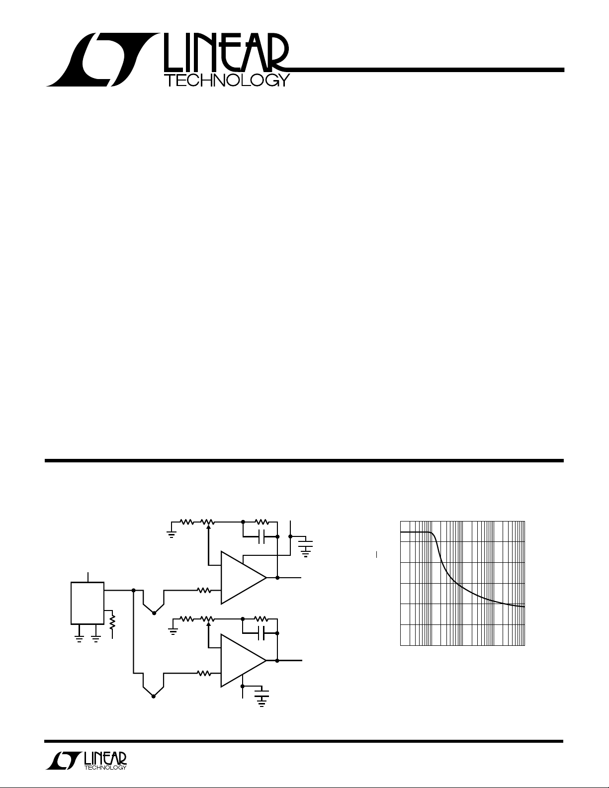
±15V Dual Thermocouple Amplifier
15V
7
V
IN
K
LT1025
GND
* FULL SCALE TRIM: TRIM FOR 10.0V OUTPUT
WITH THERMOCOUPLE AT 100°C
3
V
O
–
R
4
470k
5
–15V
–
–
+
51Ω 100Ω*
TYPE K
+
TYPE K
O
2k
2k
U
6
5
2
3
–
1/2
LTC1151
+
–
1/2
LTC1151
+
–15V
Noise Spectrum
7
1
0.1µF
15V
0.1µF
OUTPUT A
100mV/°C
OUTPUT B
100mV/°C
1151 TA01
60
50
40
30
20
NOISE VOLTAGE (nV/√Hz)
10
0
10
1 100 1k 10k
FREQUENCY (Hz)
1151 TA02
240k51Ω 100Ω*
0.1µF
8
240k
0.1µF
4
1
Page 2
LTC1151
A
W
O
LUTEXI T
S
A
WUW
ARB
U
G
I
S
(Note 1)
Total Supply Voltage (V+ to V–) ............................. 36V
Input Voltage (Note 2) ..........(V+ + 0.3V) to (V– – 0.3V)
Output Short Circuit Duration ......................... Indefinite
Burn-In Voltage ...................................................... 36V
WU
/
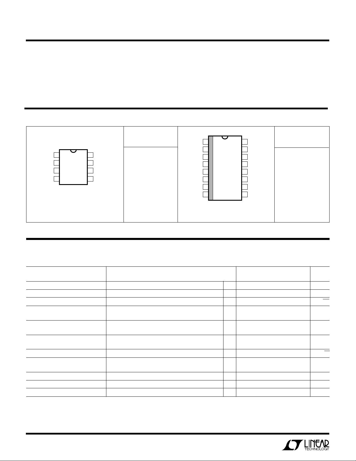
PACKAGE
OUT A
–IN A
+IN A
–
V
T
JMAX
O
RDER I FOR ATIO
TOP VIEW
1
2
3
4
N8 PACKAGE
8-LEAD PLASTIC DIP
= 110°C, θJA = 130°C/W
ORDER PART
NUMBER
V+
8
OUT B
7
–IN B
6
+IN B
5
LTC1151CN8
Operating Temperature Range
LTC1151C............................................... 0°C to 70°C
Storage Temperature Range ................ –65°C to 150°C
Lead Temperature (Soldering, 10 sec)................. 300°C
U
NC
NC
OUT A
–IN A
+IN A
NC
NC
1
2
3
4
5
–
V
6
7
8
T
JMAX
TOP VIEW
S PACKAGE
16-LEAD PLASTIC SOL
= 110°C, θJA = 200°C/W
NC
16
NC
15
+
V
14
OUT B
13
–IN B
12
+IN B
11
NC
10
NC
9
ORDER PART
NUMBER
LTC1151CS
LECTRICAL C CHARA TERIST
E
ICS
VS = ±15V, TA = Operating Temperature Range, unless otherwise specified.
LTC1151C
PARAMETER CONDITIONS MIN TYP MAX UNITS
Input Offset Voltage TA = 25°C (Note 3) ±0.5 ±5 µV
Average Input Offset Drift (Note 3) ● ±0.01 ±0.05 µV/°C
Long Term Offset Voltage Drift 50 nV/√mo
Input Offset Current T
Input Bias Current T
Input Noise Voltage R
Input Noise Current f = 10Hz (Note 4) 2.2 fA/√Hz
Input Voltage Range Positive
Common-Mode Rejection Ratio VCM = V– to 12V ● 106 130 dB
Power Supply Rejection Ratio VS = ±2.375V to ±16V ● 110 130 dB
Large-Signal Voltage Gain RL = 10k, V
= 25°C ±20 ±200 pA
A
= 25°C ±15 ±100 pA
A
= 100Ω, 0.1Hz to 10Hz 1.5 µV
S
RS = 100Ω, 0.1Hz to 1Hz 0.5 µV
Negative ● –15 –15.3 V
= ±10V ● 125 140 dB
OUT
● ±0.5 nA
● ±0.5 nA
P-P
P-P
● 12 13.2 V
2
Page 3

LTC1151
LECTRICAL C CHARA TERIST
E
VS = ±15V, TA = Operating Temperature Range, unless otherwise specified.
PARAMETER CONDITIONS MIN TYP MAX UNITS
Maximum Output Voltage Swing R
Slew Rate RL = 10k, CL = 50pF 2.5 V/µs
Gain-Bandwidth Product 2 MHz
Supply Current per Amplifier No Load, T
Internal Sampling Frequency 1000 Hz
VS = 5V, TA = Operating Temperature Range, unless otherwise specified.
Input Offset Voltage TA = 25°C (Note 3) ±0.05 ±5 µV
Average Input Offset Drift (Note 3) ● ±0.01 ±0.05 µV/°C
Long Term Offset Voltage Drift 50 nV/√mo
Input Offset Current TA = 25°C ±10 100 pA
Input Bias Current TA = 25°C ±550 pA
Input Noise Voltage R
Input Noise Current f = 10Hz (Note 4) 1.3 fA/√Hz
Input Voltage Range Positive 2.7 3.2 V
Common-Mode Rejection Ratio VCM = 0V to 2.7V 110 dB
Power Supply Rejection Ratio VS = ±2.375V to ±16V ● 110 130 dB
Large-Signal Voltage Gain RL = 10k, V
Maximum Output Voltage Swing R
Slew Rate RL = 10k, CL = 50pF 1.5 V/µs
Gain Bandwidth Product 1.5 MHz
Supply Current per Amplifier No Load, T
Internal Sampling Frequency 750 Hz
= 10k, TA = 25°C ±13.5 ±14.50 V
L
= 10k ● +10.5/–13.5 V
R
L
RL = 100k ±14.95 V
No Load ● 2.0 mA
= 100Ω, 0.1Hz to 10Hz 2.0 µV
S
RS = 100Ω, 0.1Hz to 1Hz 0.7 µV
Negative 0 – 0.3 V
= 10k to GND 4.85 V
L
RL = 100k to GND 4.97 V
ICS
LTC1151C
= 25°C 0.9 1.5 mA
A
= 0.3V to 4.5V ● 115 140 dB
OUT
= 25°C 0.5 1.0 mA
A
● 1.5 mA
P-P
P-P
The • denotes the specifications which apply over the full operating
temperature range.
Note 1: Absolute Maximum Ratings are those values beyond which life of
the device may be impaired.
Note 2: Connecting any terminal to voltages greater than V
–
may cause destructive latch-up. It is recommended that no sources
V
operating from external supplies be applied prior to power-up of the
LTC1151.
+
or less than
Note 3: These parameters are guaranteed by design. Thermocouple
effects preclude measurement of these voltage levels in high speed
automatic test systems. V
equipment capability.
Note 4: Current Noise is calculated from the formula:
IN = √(2q • Ib)
where q = 1.6 × 10
–19
is measured to a limit determined by test
OS
Coulomb.
3
Page 4

LTC1151
FREQUENCY (Hz)
40
CMRR (dB)
60
100
140
160
1 10k 100k
1k
1151 G06
0
10
120
80
20
100
VS = ±15V
LPER
Supply Current vs Supply Voltage
2.5
TA = 25°C
2.0
F
O
R
ATYPICA
UW
CCHARA TERIST
E
C
Supply Current vs Temperature
2.00
ICS
VS = ±15V
Common-Mode Input Voltage
Range vs Supply Voltage
15
TA = 25°C
10
1.5
1.0
0.5
TOTAL SUPPLY CURRENT (mA)
0
4
816
12
TOTAL SUPPLY VOLTAGE (V)
20
24
Output Short-Circuit Current vs
Supply Voltage
6
T
= 25°C
A
4
2
0
–3
–6
–9
–12
SHORT-CIRCUIT OUTPUT CURRENT (mA)
–15
12 20 28 36
8162432
4
TOTAL SUPPLY VOLTAGE, V+ TO V– (V)
V
OUT
I
SOURCE
V
OUT
I
SINK
= V–
= V+
1.75
1.50
TOTAL SUPPLY CURRENT (mA)
32
28
36
1151 G01
1.25
10 30 70
0
20
TEMPERATURE (˚C)
40
50
60
1151 G02
5
0
–5
COMMON-MODE RANGE (V)
–10
–15
0
±2.5 ±5.0 ±10.0±7.5
SUPPLY VOLTAGE (V)
±12.5
±15.0
1151 G03
Undistorted Output Swing vs
CMRR vs Frequency
1151 G04
Frequency
30
25
)
P-P
20
15
10
OUTPUT VOLTAGE (V
5
VS = ±15V
= 10k
R
L
0
100 10k 100k 1M
1k
FREQUENCY (Hz)
1151 G05
Gain and Phase vs Frequency PSRR vs Frequency
100
80
60
40
GAIN (dB)
20
0
10
100 1k 10k 100k
FREQUENCY (Hz)
4
PHASE
GAIN
VS = ±15V
= 100pF
C
L
1M 10M
1151 G07
135
90
PHASE (DEG)
45
0
–45
Gain and Phase vs Frequency
100
80
60
40
GAIN (dB)
20
0
10
100 1k 10k 100k
PHASE
GAIN
FREQUENCY (Hz)
VS = ±2.5V
= 100pF
C
L
1M 10M
1151 G08
135
90
PHASE (DEG)
45
0
–45
160
140
120
100
80
PSRR (dB)
60
40
20
0
10
1 100 1k 10k
POSITIVE
SUPPLY
NEGATIVE
SUPPLY
FREQUENCY (Hz)
VS = ±15V
100k
1151 G09
Page 5

LPER
F
O
R
ATYPICA
UW
CCHARA TERIST
E
C
LTC1151
ICS
Input Bias Current Magnitude vs
Temperature
1000
VCM = 0
= ±15V
V
S
100
10
INPUT BIAS CURRENT (pA)
1
–50
–25 0 125
25 50 75
TEMPERATURE (°C)
0.1Hz to 10Hz Noise
VS = ±15V
= 25°C
T
A
100
1151 G10
Input Bias Current Magnitude vs
Supply Voltage
18
TA = 25°C
= 0V
V
CM
15
12
9
6
INPUT BIAS CURRENT (pA)
3
0
0
±2 ±4 ±6 ±8
SUPPLY VOLTAGE (V)
±10 ±12
±14
1151 G11
±16
Input Bias Current vs
Input Common-Mode Voltage
60
45
30
15
0
–15
–30
INPUT BIAS CURRENT (pA)
–45
–60
–15
–I
B
+I
B
–5 5
–10 0
INPUT COMMON-MODE VOLTAGE (V)
VS = 15V
= 25°C
T
A
10
15
1151 G12
1µV
1s
Small-Signal Transient Response
50mV/DIV
1151 G14
VS = ±15V, AV = 1
C
= 100pF, RL = 10k
L
2ms/DIV
Large-Signal Transient Response
2V/DIV
1151 G15
V
= ±15V, AV = 1
S
C
= 100pF, RL = 10k
L
2ms/DIV 2ms/DIV
10s
1151 G13
Negative Overload Recovery
5
5V/DIV
0
0
2V/DIV
V
= ±15V, AV = –100
S
NOTE: POSITIVE OVERLOAD RECOVERY IS
TYPICALLY 3ms.
1151 G16
5
Page 6

LTC1151
100pF
100k
OUTPUT
1151 TC02
–
+
5V
7
6
4
3
2
–5V
LTC1151
10Ω
–
+
7
5
6
0.02µF
800k
–
+
3
2
800k 800k
0.04µF
0.01µF
1/2
LT1057
5V
8
1
4
–5V
1/2
LT1057
TEST CIRCUITS
Offset Voltage Test Circuit
1M
+
1k
PPLICATI
A
V
27
–
LTC1151
3
+
4
–
V
O
6
OUTPUT
R
L
1151 TC01
U
S
I FOR ATIO
WU
ACHIEVING PICOAMPERE/MICROVOLT PERFORMANCE
Picoamperes
In order to realize the picoampere level of accuracy of the
LTC1151 proper care must be exercised. Leakage currents
in circuitry external to the amplifier can significantly degrade performance. High quality insulation should be used
(e.g., Teflon); cleaning of all insulating surfaces to remove
fluxes and other residues will probably be necessary,
particularly for high temperature performance. Surface
coating may be necessary to provide a moisture barrier in
high humidity environments.
Board leakage can be minimized by encircling the input
connections with a guard ring operated at a potential close
to that of the inputs: in inverting configurations the guard
ring should be tied to ground; in noninverting connections
to the inverting input. Guarding both sides of the printed
circuit board is required. Bulk leakage reduction depends
on the guard ring width.
Microvolts
Thermocouple effects must be considered if the LTC1151’s
ultra low drift is to be fully utilized. Any connection of
dissimilar metals forms a thermoelectric junction producing an electric potential which varies with temperature
(Seebeck effect). As temperature sensors, thermocouples
exploit this phenomenon to produce useful information. In
low drift amplifier circuits the effect is a primary source of
error.
6
U
DC-10Hz Noise Test Circuit
Connectors, switches, relay contacts, sockets, resistors,
solder, and even copper wire are all candidates for thermal
EMF generation. Junctions of copper wire from different
manufacturers can generate thermal EMFs of 200nV/°C;
four times the maximum drift specification of the LTC1151.
Minimizing thermal EMF-induced errors is possible if
judicious attention is given to circuit board layout and
component selection. It is good practice to minimize the
number of junctions in the amplifier’s input signal path.
Avoid connectors, sockets, switches, and relays where
possible. In instances where this is not possible, attempt
to balance the number and type of junctions so that
differential cancellation occurs. Doing this may involve
deliberately introducing junctions to offset unavoidable
junctions.
Figure 1 is an example of the introduction of an unnecessary resistor to promote differential thermal balance.
Maintaining compensating junctions in close physical
proximity will keep them at the same temperature and
reduce thermal EMF errors.
When connectors, switches, relays and/or sockets are
necessary they should be selected for low thermal EMF
activity. The same techniques of thermally balancing and
coupling the matching junctions are effective in reducing
the thermal EMF errors of these components.
Page 7

LTC1151
PPLICATI
A
NOMINALLY UNNECESSARY
RESISTOR USED TO
THERMALLY BALANCE
OTHER INPUT RESISTOR
RESISTOR LEAD, SOLDER,
COPPER TRACE JUNCTION
Figure 1. Extra Resistors Cancel Thermal EMF
U
O
S
I FOR ATIO
LEAD WIRE/SOLDER
COPPER TRACE JUNCTION
+
LTC1151
–
WU
U
OUTPUT
1151 F01
Resistors are another source of thermal EMF errors. Table
1 shows the thermal EMF generated for different resistors.
The temperature gradient across the resistor is important,
not the ambient temperature. There are two junctions
formed at each end of the resistor and if these junctions are
at the same temperature, their thermal EMFs will cancel
each other. The thermal EMF numbers are approximate
and vary with resistor value. High values give higher
thermal EMF.
Table 1. Resistor Thermal EMF
RESISTOR TYPE THERMAL EMF/°C GRADIENT
Tin Oxide >1mV/°C
Carbon Composition ∼450µV/°C
Metal Film ∼20µV/°C
Wire Wound
Evenohm, Manganin ∼2µV/°C
PACKAGE-INDUCED OFFSET VOLTAGE
Package-induced thermal EMF effects are another important source of errors. They arise at the junctions formed
when wire or printed circuit traces contact a package lead.
Like all the previously mentioned thermal EMF effects,
they are outside the LTC1151’s offset nulling loop and
cannot be cancelled. The input offset voltage specification
of the LTC1151 is actually set by the package-induced
warm-up drift rather than by the circuit itself. The thermal
time constant ranges from 0.5 to 3 minutes, depending on
package type.
ALIASING
Like all sampled data systems, the LTC1151 exhibits
aliasing behavior at input frequencies near the sampling
frequency. The LTC1151 includes a high frequency correction loop which minimizes this effect. As a result,
aliasing is not a problem for many applications.
For a complete discussion of the correction circuitry and
aliasing behavior, please refer to the LTC1051/LTC1053
data sheet.
LOW SUPPLY OPERATION
The minimum supply for proper operation of the LTC1151
is typically 4.0V (±2.0V). In single supply applications,
PSRR is guaranteed down to 4.7V (±2.35V) to ensure
proper operation at minimum TTL supply voltage of 4.75V.
U
O
1M
SA
High Voltage Instrumentation Amplifier
1k
+
–IN
2
3
–
1/2
LTC1151
+
V
0.1µF
8
1
1k
+IN
6
5
1M
–
1/2
LTC1151
+
7
GAIN = 1000V/V
4
OUTPUT OFFSET < 5mA
0.1µF
–
V
V
OUT
1151 TA03
7
PPLICATITYPICAL
Information furnished by Linear Technology Corporation is believed to be accurate and reliable.
However, no responsibility is assumed for its use. Linear Technology Corporation makes no representation that the interconnection of circuits as described herein will not infringe on existing patent rights.
Page 8

LTC1151
U
O
PPLICATITYPICAL
SA
Bridge Amplifier with Active Common-Mode Suppression
PACKAGEDESCRIPTI
0.300 – 0.320
(7.620 – 8.128)
15V
1/2
LTC1151
–15V
O
15V
499Ω
49.9k
–
LTC1151
+
1/2
350Ω TRIM TO SET
BRIDGE OPERATING
0.1µF
–
CURRENT
350Ω
STRAIN
GAUGE
+
0.1µF
390Ω
–15V
U
Dimensions in inches (millimeters) unless otherwise noted.
N8 Package, 8-Lead Plastic DIP
0.045 – 0.065
(1.143 – 1.651)
0.130 ± 0.005
(3.302 ± 0.127)
0.400
(10.160)
MAX
876
V
OUT
A
V
1151 TA04
= 100
5
0.065
(1.651)
0.009 – 0.015
(0.229 – 0.381)
+0.025
0.325
–0.015
+0.635
8.255
()
–0.381
TYP
0.045 ± 0.015
(1.143 ± 0.381)
0.100 ± 0.010
(2.540 ± 0.254)
(0.457 ± 0.076)
S Package, 16-Lead SOL
0.291 – 0.299
(7.391 – 7.595)
0.005
(0.127)
RAD MIN
0.009 – 0.013
(0.229 – 0.330)
NOTE:
PIN 1 IDENT, NOTCH ON TOP AND CAVITIES ON THE BOTTOM OF PACKAGES ARE THE MANUFACTURING OPTIONS.
THE PART MAY BE SUPPLIED WITH OR WITHOUT ANY OF THE OPTIONS.
0.010 – 0.029
(0.254 – 0.737)
SEE NOTE
0.016 – 0.050
(0.406 – 1.270)
× 45°
0° – 8° TYP
0.093 – 0.104
(2.362 – 2.642)
0.050
(1.270)
TYP
0.014 – 0.019
(0.356 – 0.482)
TYP
Linear Technology Corporation
8
1630 McCarthy Blvd., Milpitas, CA 95035-7487
(408) 432-1900
●
FAX
: (408) 434-0507
●
TELEX
: 499-3977
0.125
(3.175)
MIN
0.018 ± 0.003
0.037 – 0.045
(0.940 – 1.143)
0.020
(0.508)
MIN
0.004 – 0.012
(0.102 – 0.305)
SEE NOTE
0.250 ± 0.010
(6.350 ± 0.254)
1234
0.398 – 0.413
(10.109 – 10.490)
15 1413121110 9
16
2345678
1
LINEAR TECHNOLOGY CORPORATION 1993
0.394 – 0.419
(10.007 – 10.643)
LT/GP 0193 10K REV 0
 Loading...