

Datasheet LTC1098LIS8, LTC1098LCS8, LTC1098IS8, LTC1096LCS8, LTC1096IN8 Datasheet (Linear Technology)
...Page 1
LTC1096/LTC1096L
SAMPLE FREQUENCY, f
SMPL
(kHz)
0.1
1
SUPPLY CURRENT, I
CC
(µA)
10
100
1000
1 10 100
LTC1096/98 • TPC03
TA = 25°C
V
CC
= V
REF
= 5V
LTC1098/LTC1098L
Micropower Sampling
8-Bit Serial I/O A/D Converters
EATU
F
■
80µA Maximum Supply Current
■
1nA Typical Supply Current in Shutdown
■
8-Pin SO Plastic Package
■
5V Operation (LTC1096/LTC1098)
■
3V Operation (LTC1096L/LTC1098L)(2.65V Min)
■
Sample-and-Hold
■
16µs Conversion Time
■
33kHz Sample Rate
■
±0.5LSB Total Unadjusted Error Over Temp
■
Direct 3-Wire Interface to Most MPU Serial Ports and
RE
S
All MPU Parallel I/O Ports
U
O
PPLICATI
A
■
Battery-Operated Systems
■
Remote Data Acquisition
■
Battery Monitoring
■
Battery Gas Gauges
■
Temperature Measurement
■
Isolated Data Acquisition
, LTC and LT are registered trademarks of Linear Technology Corporation.
S
DUESCRIPTIO
The LTC®1096/LTC1096L/LTC1098/LTC1098L are
micropower, 8-bit A/D converters that draw only 80µ A of
supply current when converting. They automatically power
down to 1nA typical supply current whenever they are not
performing conversions. They are packaged in 8-pin SO
packages and have both 3V (L) and 5V versions. These
8-bit, switched-capacitor, successive approximation ADCs
include sample-and-hold. The LTC1096/LTC1096L have a
single differential analog input. The LTC1098/LTC1098L
offer a software selectable 2-channel MUX.
On-chip serial ports allow efficient data transfer to a wide
range of microprocessors and microcontrollers over three
wires. This, coupled with micropower consumption, makes
remote location possible and facilitates transmitting data
through isolation barriers.
These circuits can be used in ratiometric applications or
with an external reference. The high impedance analog
inputs and the ability to operate with reduced spans
(below 1V full scale) allow direct connection to sensors
and transducers in many applications, eliminating the
need for gain stages.
ANALOG INPUT
0V TO 5V RANGE
U
O
A
PPLICATITYPICAL
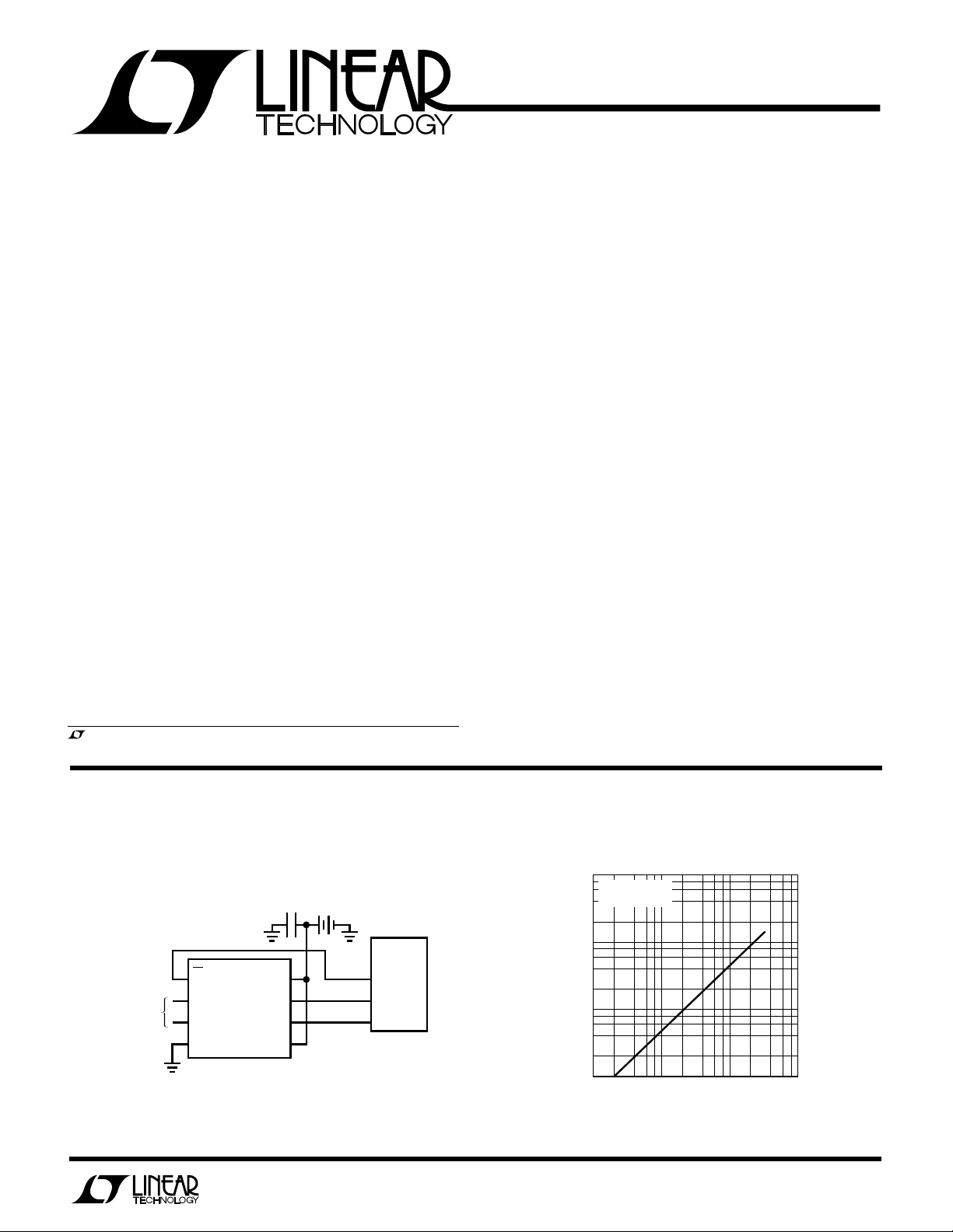
10µW, S8 Package, 8-Bit A/D
Samples at 200Hz and Runs Off a 5V Battery
5V1µF
CS/
SHUTDOWN
+IN
–IN
GND
LTC1096
V
CC
CLK
D
OUT
V
REF
MPU
(e.g., 8051)
P1.4
P1.3
P1.2
LTC1096/8 • TA01
Supply Current vs Sample Rate
1
Page 2
LTC1096/LTC1096L
LTC1098/LTC1098L
A
W
O
LUTEXI T
S
A
WUW
ARB
U
G
I
S
(Notes 1 and 2)
Supply Voltage (VCC) to GND................................... 12V
Voltage
Analog and Reference ................ –0.3V to V
CC
+ 0.3V
Digital Inputs......................................... –0.3V to 12V
Digital Outputs ........................... –0.3V to V
CC
+ 0.3V
Power Dissipation.............................................. 500mW
Storage Temperature Range ................. –65°C to 150°C
WU
/
PACKAGE
CS/
SHUTDOWN
1096
1096A
+IN
–IN
GND
N8 PACKAGE
8-LEAD PLASTIC DIP
T
JMAX
T
JMAX
S8 PART MARKING
O
RDER I FOR ATIO
TOP VIEW
1
2
3
4
8-LEAD PLASTIC SOIC
= 150°C, θJA = 130°C/W (N8)
= 150°C, θJA = 175°C/W (S8)
1096I
1096IA
V
8
CLK
7
D
6
V
5
S8 PACKAGE
1096L
1096LI
CC
OUT
REF
ORDER PART
NUMBER
LTC1096ACN8
LTC1096ACS8
LTC1096AIN8
LTC1096AIS8
LTC1096CN8
LTC1096CS8
LTC1096IN8
LTC1096IS8
LTC1096LCS8
LTC1096LIS8
Operating Temperature
LTC1096AC/LTC1096C/LTC1096LC/
LTC1098AC/LTC1098C/LTC1098LC ....... 0°C to 70°C
LTC1096AI/LTC1096I/LTC1096LI/
LTC1098AI/LTC1098I/LTC1098LI ..... –40°C to 85°C
Lead Temperature (Soldering, 10 sec.)................ 300°C
U
(Notes 3)
TOP VIEW
CS/
SHUTDOWN
8-LEAD PLASTIC DIP
1
2
CH0
3
CH1
4
GND
N8 PACKAGE
T
= 150°C, θJA = 130°C/W (N8)
JMAX
= 150°C, θJA = 175°C/W (S8)
T
JMAX
S8 PART MARKING
1098
1098A
1098I
1098IA
V
8
CC(VREF)
CLK
7
D
6
OUT
D
5
IN
S8 PACKAGE
8-LEAD PLASTIC SOIC
1098L
1098LI
ORDER PART
LTC1098ACN8
LTC1098ACS8
LTC1098AIN8
LTC1098AIS8
LTC1098CN8
LTC1098CS8
LTC1098IN8
LTC1098IS8
LTC1098LCS8
LTC1098LIS8
NUMBER
Consult factory for Military grade parts.
WUW
UUU
RECO E DED OPERATI G CO DITIO S
LTC1096/LTC1098
SYMBOL PARAMETER CONDITIONS MIN TYP MAX UNITS
V
CC
VCC = 5V Operation
f
CLK
t
CYC
t
hDI
t
suCS
t
WAKEUP
t
suDI
t
WHCLK
Supply Voltage LTC1096 3.0 9 V
Clock Frequency VCC = 5V 25 500 kHz
Total Cycle Time LTC1096, f
Hold Time, DIN After CLK↑ VCC = 5V 150 ns
Setup Time CS↓ Before First CLK↑ (See Operating Sequence) VCC = 5V, LTC1096 500 ns
Wake-Up Time CS↓ Before First CLK↓ After First CLK↑ VCC = 5V, LTC1096 10 µs
(See Figure 1 LTC1096 Operating Sequence)
Wake-Up Time CS↓ Before MSBF Bit CLK↓ VCC = 5V, LTC1098 10 µs
(See Figure 2 LTC1098 Operating Sequence)
Setup Time, DIN Stable Before CLK↑ VCC = 5V 400 ns
CLK High Time VCC = 5V 0.8 µs
LTC1098 3.0 6 V
= 500kHz 29 µs
LTC1098, f
VCC = 5V, LTC1098 500 ns
CLK
= 500kHz 29 µs
CLK
2
Page 3
LTC1096/LTC1096L
LTC1098/LTC1098L
WUW
UUU
RECO E DED OPERATI G CO DITIO S
LTC1096/LTC1098
SYMBOL PARAMETER CONDITIONS MIN TYP MAX UNITS
t
WLCLK
t
WHCS
t
WLCS
VCC = 3V Operation
f
CLK
t
CYC
t
hDI
t
suCS
t
WAKEUP
t
suDI
t
WHCLK
t
WLCLK
t
WHCS
t
WLCS
CLK Low Time VCC = 5V 0.8 µs
CS High Time Between Data Transfer Cycles VCC = 5V 1 µs
CS Low Time During Data Transfer LTC1096, f
LTC1098, f
Clock Frequency VCC = 3V 25 250 kHz
Total Cycle Time LTC1096, f
LTC1098, f
Hold Time, DIN After CLK↑ VCC = 3V 450 ns
Setup Time CS↓ Before First CLK↑ (See Operating Sequence) VCC = 3V, LTC1096 1 µs
VCC = 3V, LTC1098 1 µs
Wake-Up Time CS↓ Before First CLK↓ After First CLK↑ VCC = 3V, LTC1096 10 µs
(See Figure 1 LTC1096 Operating Sequence)
Wake-Up Time CS↓ Before MSBF Bit CLK↓ VCC = 3V, LTC1098 10 µs
(See Figure 2 LTC1098 Operating Sequence)
Setup Time, DIN Stable Before CLK↑ VCC = 3V 1 µs
CLK High Time VCC = 3V 1.6 µs
CLK Low Time VCC = 3V 1.6 µs
CS High Time Between Data Transfer Cycles VCC = 3V 2 µs
CS Low Time During Data Transfer LTC1096, f
LTC1098, f
= 500kHz 28 µs
CLK
= 500kHz 28 µs
CLK
= 250kHz 58 µs
CLK
= 250kHz 58 µs
CLK
= 250kHz 56 µs
CLK
= 250kHz 56 µs
CLK
LTC1096L/LTC1098L
SYMBOL PARAMETER CONDITIONS MIN TYP MAX UNITS
V
CC
f
CLK
t
CYC
t
hDI
t
suCS
t
WAKEUP
t
suDI
t
WHCLK
t
WLCLK
t
WHCS
t
WLCS
Supply Voltage 2.65 4.0 V
Clock Frequency VCC = 2.65V 25 250 kHz
Total Cycle Time LTC1096L, f
Hold Time, DIN After CLK↑ VCC = 2.65V 450 ns
Setup Time CS↓ Before First CLK↑ (See Operating Sequence) VCC = 2.65V, LTC1096L 1 µs
Wake-Up Time CS↓ Before First CLK↓ After First CLK↑ VCC = 2.65V, LTC1096L 10 µs
(See Figure 1, LTC1096L Operating Sequence)
Wake-Up Time CS↓ Before MSBF Bit CLK↓ VCC = 2.65V, LTC1098L 10 µs
(See Figure 2, LTC1098L Operating Sequence)
Setup Time, DIN Stable Before CLK↑ VCC = 2.65V 1 µs
CLK High Time VCC = 2.65V 1.6 µs
CLK Low Time VCC = 2.65V 1.6 µs
CS High Time Between Data Transfer Cycles VCC = 2.65V 2 µs
CS Low Time During Data Transfer LTC1096L, f
LTC1098L, f
V
= 2.65V, LTC1098L 1 µs
CC
LTC1098L, f
= 250kHz 58 µs
CLK
= 250kHz 58 µs
CLK
= 250kHz 56 µs
CLK
= 250kHz 56 µs
CLK
3
Page 4
LTC1096/LTC1096L
LTC1098/LTC1098L
UU W
CO VERTER A D ULTIPLEXER CHARACTERISTICS
LTC1096/LTC1098
VCC = 5V, V
PARAMETER CONDITIONS MIN TYP MAX MIN TYP MAX UNITS
Resolution (No Missing Code) ● 8 8 Bits
Offset Error ● ±0.5 ±0.5 LSB
Linearity Error (Note 4) ● ±0.5 ±0.5 LSB
Full Scale Error ● ±0.5 ±1.0 LSB
Total Unadjusted Error (Note 5) V
Analog Input Range (Notes 6, 7) V
REF Input Range (Notes 6, 7) 4.5 ≤ VCC ≤ 6V V
Analog Input Leakage Current (Note 8) ● ±1.0 ±1.0 µA
LTC1096/LTC1098
VCC = 3V, V
PARAMETER CONDITIONS MIN TYP MAX MIN TYP MAX UNITS
Resolution (No Missing Code) ● 8 8 Bits
Offset Error ● ±0.75 ±1.0 LSB
Linearity Error (Notes 4, 9) ● ±0.5 ±1.0 LSB
Full-Scale Error ● ±1.0 ±1.0 LSB
Total Unadjusted Error
Analog Input Range (Notes 6, 7) V
REF Input Range (Notes 6, 7, 9) 3V ≤ VCC ≤ 6V V
Analog Input Leakage Current (
= 5V, f
REF
= 2.5V, f
REF
= 500kHz, unless otherwise noted.
CLK
= 5.000V ● ±0.5 ±1.0 LSB
REF
6V < VCC ≤ 9V, LTC1096 V
= 250kHz, unless otherwise noted.
CLK
(Notes 5, 9)
V
= 2.500V ● ±1.0 ±1.5 LSB
REF
Notes 8, 9
)
LTC1096A/LTC1098A
–0.05V to VCC + 0.05V
–0.05V to V
–0.05V to 6V
–0.05V to VCC + 0.05V
–0.05V to V
● ±1.0 ±1.0 µ A
LTC1096/LTC1098
+ 0.05V
CC
LTC1096/LTC1098LTC1096A/LTC1098A
+ 0.05V
CC
LTC1096L/LTC1098L
VCC = 2.65V, V
PARAMETER CONDITIONS MIN TYP MAX UNITS
Resolution (No Missing Code) ● 8 Bits
Offset Error ● ±1.0 LSB
Linearity Error (Note 4) ● ±1.0 LSB
Full-Scale Error ● ±1.0 LSB
Total Unadjusted Error
Analog Input Range (Notes 6, 7) –0.05V to VCC + 0.05V V
REF Input Range (Note 6) 2.65V ≤ VCC ≤ 4.0V –0.05V to VCC + 0.05V V
Analog Input Leakage Current (Note 8) ● ±1.0 µA
= 2.5V, f
REF
(Notes 5)
= 250kHz, unless otherwise noted.
CLK
V
= 2.5V ● ±1.5 LSB
REF
LTC1096L/LTC1098L
4
Page 5
LTC1096/LTC1096L
LTC1098/LTC1098L
U
DIGITAL AND DC ELECTRICAL CHARACTERISTICS
LTC1096/LTC1098
VCC = 5V, V
SYMBOL PARAMETER CONDITIONS MIN TYP MAX UNITS
V
IH
V
IL
I
IH
I
IL
V
OH
V
OL
I
OZ
I
SOURCE
I
SINK
I
REF
I
CC
= 5V, unless otherwise noted.
REF
High Level Input Voltage VCC = 5.25V ● 2.0 V
Low Level Input Voltage VCC = 4.75V ● 0.8 V
High Level Input Current VIN = V
CC
● 2.5 µA
Low Level Input Current VIN = 0V ● –2.5 µA
High Level Output Voltage VCC = 4.75V, IO = 10µA ● 4.5 4.74 V
VCC = 4.75V, IO = 360µA ● 2.4 4.72 V
Low Level Output Voltage VCC = 4.75V, IO = 1.6mA ● 0.4 V
Hi-Z Output Leakage CS ≥ V
Output Source Current V
Output Sink Current V
= 0V –25 mA
OUT
= V
OUT
Reference Current CS = V
≥ 200µs, f
t
CYC
t
= 29µs, f
CYC
Supply Current CS = V
LTC1096, t
LTC1096, t
LTC1098, t
LTC1098, t
IH
CC
CC
CC
≤ 50kHz ● 3.500 7.5 µA
CLK
= 500kHz ● 35.000 50.0 µA
CLK
≥ 200µs, f
CYC
= 29µs, f
CYC
≥ 200µs, f
CYC
= 29µs, f
CYC
≤ 50kHz ● 40 80 µA
CLK
= 500kHz ● 120 180 µA
CLK
≤ 50kHz ● 44 88 µA
CLK
= 500kHz ● 155 230 µA
CLK
● ±3.0 µA
45 mA
● 0.001 2.5 µA
● 0.001 3.0 µA
LTC1096/LTC1098
VCC = 3V, V
SYMBOL PARAMETER CONDITIONS MIN TYP MAX UNITS
V
IH
V
IL
I
IH
I
IL
V
OH
V
OL
I
OZ
I
SOURCE
I
SINK
I
REF
I
CC
= 2.5V, unless otherwise noted.
REF
High Level Input Voltage VCC = 3.6V ● 1.9 V
Low Level Input Voltage VCC = 3V ● 0.45 V
High Level Input Current (Note 9) VIN = V
CC
● 2.5 µA
Low Level Input Current (Note 9) VIN = 0V ● –2.5 µA
High Level Output Voltage VCC = 3V, IO = 10µA ● 2.3 2.69 V
VCC = 3V, IO = 360µA ● 2.1 2.64 V
Low Level Output Voltage VCC = 3V, IO = 400µA ● 0.3 V
Hi-Z Output Leakage (Note 9) CS ≥ V
Output Source Current (Note 9) V
Output Sink Current (Note 9) V
= 0V –10 mA
OUT
= V
OUT
Reference Current (Note 9) CS = V
t
≥ 200µs, f
CYC
= 58µs, f
t
CYC
Supply Current (Note 9) CS = V
LTC1096, t
LTC1096, t
LTC1098, t
LTC1098, t
IH
CC
CC
CC
≤ 50kHz ● 3.500 7.5 µA
CLK
= 250kHz ● 35.000 50.0 µA
CLK
≥ 200µs, f
CYC
= 58µs, f
CYC
≥ 200µs, f
CYC
= 58µs, f
CYC
≤ 50kHz ● 40 80 µA
CLK
= 250kHz ● 120 180 µA
CLK
≤ 50kHz ● 44 88 µA
CLK
= 250kHz ● 155 230 µA
CLK
● ±3.0 µA
15 mA
● 0.001 2.5 µA
● 0.001 3.0 µA
5
Page 6
LTC1096/LTC1096L
LTC1098/LTC1098L
U
DIGITAL AND DC ELECTRICAL CHARACTERISTICS
LTC1096L/LTC1098L
VCC = 2.65V, V
SYMBOL PARAMETER CONDITIONS MIN TYP MAX UNITS
V
IH
V
IL
I
IH
I
IL
V
OH
V
OL
I
OZ
I
SOURCE
I
SINK
I
REF
I
CC
= 2.5V, f
REF
= 250kHz, unless otherwise noted.
CLK
High Level Input Voltage VCC = 3.6V ● 1.9 V
Low Level Input Voltage VCC = 2.65V ● 0.45 V
High Level Input Current VIN = V
CC
● 2.5 µA
Low Level Input Current VIN = 0V ● –2.5 µA
High Level Output Voltage VCC = 2.65V, IO = 10µA ● 2.3 2.64 V
= 2.65V, IO = 360µA ● 2.1 2.50 V
V
CC
Low Level Output Voltage VCC = 2.65V, IO = 400µA ● 0.3 V
Hi-Z Output Leakage CS = High ● ±3.0 µA
Output Source Current V
Output Sink Current V
Reference Current CS = V
Supply Current CS = V
= 0V –10 mA
OUT
= V
OUT
CC
CC
≥ 200µs, f
t
CYC
= 58µs, f
t
CYC
CC
LTC1096L, t
LTC1096L, t
LTC1098L, t
LTC1098L, t
● 0.001 2.5 µA
≤ 50kHz ● 3.500 7.5 µA
CLK
= 250kHz ● 35.000 50.0 µ A
CLK
● 0.001 3.0 µA
≥ 200µs, f
CYC
= 58µs, f
CYC
≥ 200µs, f
CYC
= 58µs, f
CYC
≤ 50kHz ● 40 80 µA
CLK
= 250kHz ● 120 180 µA
CLK
≤ 50kHz ● 44 88 µA
CLK
= 250kHz ● 155 230 µA
CLK
15 mA
AC CHARACTERISTICS
LTC1096/LTC1098
VCC = 5V, V
SYMBOL PARAMETER CONDITIONS MIN TYP MAX UNITS
t
SMPL
f
SMPL
(MAX)
t
CONV
t
dDO
t
dis
t
en
t
hDO
t
f
t
r
C
IN
REF
= 5V, f
= 500kHz, unless otherwise noted.
CLK
Analog Input Sample Time See Operating Sequence 1.5 CLK Cycles
Maximum Sampling Frequency ● 33 kHz
Conversion Time See Operating Sequence 8 CLK Cycles
Delay Time, CLK↓ to D
Delay Time, CS↑ to D
Delay Time, CLK↓ to D
Time Output Data Remains Valid After CLK↓ C
D
Fall Time See Test Circuits ● 70 250 ns
OUT
D
Rise Time See Test Circuits ● 25 100 ns
OUT
Data Valid See Test Circuits ● 200 450 ns
OUT
Hi-Z See Test Circuits ● 170 450 ns
OUT
Enable See Test Circuits ● 60 250 ns
OUT
= 100pF 180 ns
LOAD
Input Capacitance Analog Inputs On Channel 25 pF
Analog Inputs Off Channel 5 pF
Digital Input 5 pF
6
Page 7
LTC1096/LTC1096L
LTC1098/LTC1098L
AC CHARACTERISTICS
LTC1096/LTC1098
VCC = 3V, V
SYMBOL PARAMETER CONDITIONS MIN TYP MAX UNITS
t
SMPL
f
SMPL(MAX)
t
CONV
t
dDO
t
dis
t
en
t
hDO
t
f
t
r
C
IN
= 2.5V, f
REF
= 250kHz, unless otherwise noted.
CLK
Analog Input Sample Time See Operating Sequence 1.5 CLK Cycles
Maximum Sampling Frequency ● 16.5 kHz
Conversion Time See Operating Sequence 8 CLK Cycles
Delay Time, CLK↓ to D
Delay Time, CS↑ to D
Delay Time, CLK↓ to D
Time Output Data Remains Valid After CLK↓ C
D
Fall Time See Test Circuits (Note 9) ● 70 250 ns
OUT
D
Rise Time See Test Circuits (Note 9) ● 50 150 ns
OUT
Data Valid See Test Circuits (Note 9) ● 500 1000 ns
OUT
Hi-Z See Test Circuits (Note 9) ● 220 800 ns
OUT
Enable See Test Circuits (Note 9) ● 160 480 ns
OUT
= 100pF 400 ns
LOAD
Input Capacitance Analog Inputs On Channel 25 pF
Analog Inputs Off Channel 5 pF
Digital Input 5 pF
LTC1096L/LTC1098L
VCC = 2.65V, V
SYMBOL PARAMETER CONDITIONS MIN TYP MAX UNITS
t
SMPL
f
SMPL(MAX)
t
CONV
t
dDO
t
dis
t
en
t
hDO
t
f
t
r
C
IN
The ● denotes specifications which apply over the operating temperature
range.
Note 1: Absolute Maximum Ratings are those values beyond which the life
of a device may be impaired.
Note 2: All voltage values are with respect to GND.
Note 3: For the 8-lead PDIP, consult the factory.
Note 4: Linearity error is specified between the actual and points of the
A/D transfer curve.
Note 5: Total unadjusted error includes offset, full scale, linearity,
multiplexer and hold step errors.
Note 6: Two on-chip diodes are tied to each reference and analog input
which will conduct for reference or analog input voltages one diode drop
below GND or one diode drop above V
bias of either diode. This means that as long as the reference or analog
= 2.5V, f
REF
= 250kHz, unless otherwise noted.
CLK
Analog Input Sample Time See Operating Sequence 1.5 CLK Cycles
Maximum Sampling Frequency ● 16.5 kHz
Conversion Time See Operating Sequence 8 CLK Cycles
Delay Time, CLK↓ to D
Delay Time, CS↑ to D
Delay Time, CLK↓ to D
Time Output Data Remains Valid After CLK↓ C
D
Fall Time See Test Circuits ● 70 250 ns
OUT
D
Rise Time See Test Circuits ● 50 200 ns
OUT
Data Valid See Test Circuits ● 500 1000 ns
OUT
Hi-Z See Test Circuits ● 220 800 ns
OUT
Enable See Test Circuits ● 160 480 ns
OUT
= 100pF 400 ns
LOAD
Input Capacitance Analog Inputs On Channel 25 pF
Analog Inputs Off Channel 5 pF
Digital Input 5 pF
input does not exceed the supply voltage by more than 50mV, the output
code will be correct. To achieve an absolute 0V to 5V input voltage range
will therefore require a minimum supply voltage of 4.950V over initial
tolerance, temperature variations and loading. For 5.5V < V
CC
≤ 9V,
reference and analog input range cannot exceed 5.55V. If reference and
analog input range are greater than 5.55V, the output code will not be
guaranteed to be correct.
Note 7: The supply voltage range for the LTC1096L/LTC1098L is from
2.65V to 4V. The supply voltage range for the LTC1096 is from 3V to 9V,
but the supply voltage range for the LTC1098 is only from 3V to 6V.
Note 8: Channel leakage current is measured after the channel selection.
Note 9: These specifications are either correlated from 5V specifications or
. This spec allows 50mV forward
CC
guaranteed by design.
7
Page 8
LTC1096/LTC1096L
REFERENCE VOLTAGE (V)
0
CHANGE IN LINEARITY (LSB)
0
0.25
4
LTC1096/98 • TPC06
–0.25
–O.50
1
2
3
5
0.50
TA = 25°C
V
CC
= 5V
F
CLK
= 500kHz
VOLTAGE REFERENCE (V)
0
CHANGE IN GAIN (LSB)
0
0.25
4
LTC1096/98 • TPC09
–0.25
–O.50
1
2
3
5
0.50
TA = 25°C
V
CC
= 5V
F
CLK
= 500kHz
LTC1098/LTC1098L
LPER
F
O
R
ATYPICA
UW
CCHARA TERIST
E
C
ICS
Supply Current vs Clock Rate
for Active and Shutdown Modes
250
TA = 25°C
CS = 0V
200
150
(µA)
CC
100
50
10
SUPPLY CURRENT, I
0.002
0
1
CS = V
10 100 1000
FREQUENCY (kHz)
Change in Offset vs
Reference Voltage LTC1096
)
REF
0.50
0.25
0
–0.25
–0.50
MAGNITUDE OF OFFSET CHANGE (LSB = 1/256 × V
1
0
2
REFERENCE VOLTAGE (V)
Change in Linearity vs
Supply Voltage
0.5
0.4
0.3
0.2
0.1
0
–0.1
–0.2
CHANGE IN LINEARTY (LSB)
–0.3
–0.4
–0.5
19
0
3
2
SUPPLY VOLTAGE, VCC (V)
5
4
100
VCC = 9V
(µA)
VCC = 5V
CC
LTC1096/98 • TPC01
TA = 25°C
= 5V
V
CC
= 500kHz
F
CLK
3
4
5
LTC1096/98 • TPC04
T
= 25°C
A
= 2.5V
V
REF
= 100kHz
F
CLK
7
6
8
10
LTC1096/98 • TPC07
CC
SUPPLY CURRENT, I
0.001
–0.1
–0.2
–0.3
–0.4
MAGNITUDE OF OFFSET CHANGE (LSB)
–0.5
–0.1
–0.2
CHANGE IN GAIN (LSB)
–0.3
–0.4
–0.5
Supply Current vs Supply Voltage
Active and Shutdown Modes
T
= 25°C
A
V
REF
80
60
40
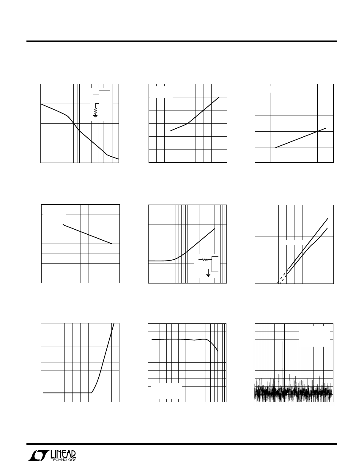
20
0
13
0
= 2.5V
“ACTIVE” MODE CS = 0
“SHUTDOWN” MODE CS = V
2
SUPPLY VOLTAGE,VCC (V)
59
4
7
6
LTC1096/98 • TPC02
CC
8
1000
(µA)
100
CC
SUPPLY CURRENT, I
Change in Offset vs
Supply Voltage
0.5
0.4
0.3
0.2
0.1
0
3
2
19
0
4
SUPPLY VOLTAGE, VCC (V)
T
= 25°C
A
= 2.5V
V
REF
= 100kHz
F
CLK
7
6
8
5
LTC1096/98 • TPC05
10
Change in Gain vs Supply Voltage
0.5
0.4
0.3
0.2
0.1
0
3
2
19
0
4
SUPPLY VOLTAGE, VCC (V)
T
= 25°C
A
= 2.5V
V
REF
= 100kHz
F
CLK
7
6
8
5
10
LTC1096/98 • TPC08
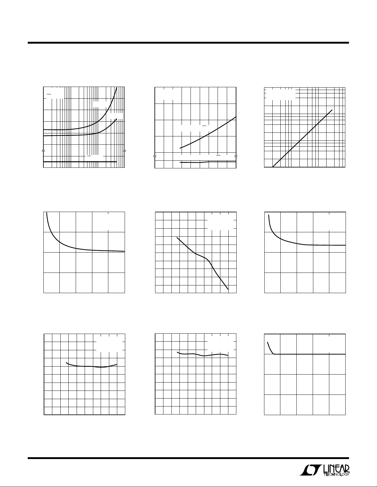
Supply Current vs Sample
Frequency LTC1096
TA = 25°C
= V
V
10
1
0.1
= 5V
CC
REF
1 10 100
SAMPLE FREQUENCY, f
SMPL
Change in Linearity vs
Reference Voltage LTC1096
Change in Gain vs
Reference Voltage LTC1096
(kHz)
LTC1096/98 • TPC03
8
Page 9
TEMPERATURE (°C)
–60
LEAKAGE CURRENT (nA)
10
100
1000
100
LTC1096/98 • TPC15
1
0.1
0.01
–20
20
60
140
–40 0
40
80 120
V
REF
= 5V
V
CC
= 5V
ON CHANNEL
OFF CHANNEL
FREQUENCY (kHz)
0
–100
AMPLITUDE (dB)
–90
–70
–60
–50
0
–30
2
4
LTC1096/98 • TPC18
–80
–20
–10
–40
6
8
10 12
14 16
TA = 25°C
V
CC
= V
REF
= 5V
f
SMPL
= 31.25kHz
f
IN
= 5.8kHz
LPER
F
O
R
ATYPICA
UW
CCHARA TERIST
E
C
LTC1096/LTC1096L
LTC1098/LTC1098L
ICS
Maximum Clock Frequency vs
Source Resistance
1
TA = 25°C
= V
V
0.75
0.50
0.25
MAXIMUM CLOCK FREQUENCY* (MHz)
0
1
= 5V
CC
REF
R
SOURCE
V
IN
10 100
–
(kΩ)
Wake-Up Time vs Supply Voltage
4
TA = 25°C
= 2.5V
V
REF
3
+ INPUT
– INPUT
–
R
SOURCE
LTC1096/98 • TPC10
Maximum Clock Frequency vs
Supply Voltage
1.5
TA = 25°C
= 2.5V
V
REF
1.25
1.0
0.75
0.5
0.25
MAXIMUM CLOCK FREQUENCY (MHz)
0
0
2468
SUPPLY VOLTAGE (V)
Minimum Wake-Up Time
vs Source Resistance
10
TA = 25°C
= 5V
V
REF
7.5
LTC1096/98 • TPC11
Digital Input Logic Threshold
vs Supply Voltage
5
TA = 25°C
4
3
2
LOGIC THRESH0LD (V)
1
10
0
2
0
SUPPLY VOLTAGE, VCC (V)
6
8
4
10
LTC1096/98 • TPC12
Input Channel Leakage Current
vs Temperature
2
WAKE-UP TIME (µs)
1
0
0
Minimum Clock Frequency for
0.1LSB Error† vs Temperature
200
180
160
140
120
100
80
60
40
MINIMUM CLOCK FREQUENCY (kHz)
20
0
–60
* Maximum CLK frequency represents the clock frequency at which a 0.1LSB shift in the error at any code
transition from its 0.75MHz value is first detected.
†
As the CLK frequency is decreased from 500kHz, minimum CLK frequency (∆error ≤ 0.1LSB) represents
the frequency at which a 0.1LSB shift in any code transition from its 500kHz value is first detected.
2
SUPPLY VOLTAGE, VCC (V)
V
= 5V
REF
= 5V
V
CC
–20
–40 0
20
TEMPERATURE (°C)
4
40
6
60
80 120
8
LTC1096/98 • TPC13
100
•
10
140
5.0
2.5
MINIMUM WAKE-UP TIME (µs)
0
1
ENOBs vs Frequency
10
9
8
7
6
5
ENOBs
4
3
2
TA = 25°C
= V
V
CC
1
f
SMPL
REF
= 31.25kHz
1
0
V
10 100
R
(kΩ)
SOURCE
= 5V
10 100
FREQUENCY (kHz)
R
SOURCE
IN
LTC1096/98 • TPC17
+
+
–
LTC1096/98 • TPC14
FFT Plot
9
Page 10

LTC1096/LTC1096L
LTC1098/LTC1098L
U
UU
PI FU CTIO S
LTC1096/LTC1096L
CS/SHDN (Pin 1): Chip Select Input. A logic low on this
input enables the LTC1096/LTC1096L. A logic high on this
input disables the LTC1096/LTC1096L and disconnects
the power to the LTC1096/LTC1096L.
IN+ (Pin 2): Analog Input. This input must be free of noise
with respect to GND.
IN– (Pin 3): Analog Input. This input must be free of noise
with respect to GND.
GND (Pin 4): Analog Ground. GND should be tied directly
to an analog ground plane.
V
(Pin 5): Reference Input. The reference input defines
REF
the span of the A/D converter and must be kept free of
noise with respect to GND.
D
(Pin 6): Digital Data Output. The A/D conversion
OUT
result is shifted out of this output.
CLK (Pin 7): Shift Clock. This clock synchronizes the serial
data transfer.
VCC (Pin 8): Power Supply Voltage. This pin provides
power to the A/D converter. It must be free of noise and
ripple by bypassing directly to the analog ground plane.
LTC1098/LTC1098L
CS/SHDN (Pin 1): Chip Select Input. A logic low on this
input enables the LTC1098/LTC1098L. A logic high on this
input disables the LTC1098/LTC1098L and disconnects
the power to the LTC1098/LTC1098L.
CH0 (Pin 2): Analog Input. This input must be free of noise
with respect to GND.
CH1 (Pin 3): Analog Input. This input must be free of noise
with respect to GND.
GND (Pin 4): Analog Ground. GND should be tied directly
to an analog ground plane.
DIN (Pin 5): Digital Data Input. The multiplexer address is
shifted into this pin.
D
(Pin 6): Digital Data Output. The A/D conversion
OUT
result is shifted out of this output.
CLK (Pin 7): Shift Clock. This clock synchronizes the serial
data transfer.
VCC (V
vides power and defines the span of the A/D converter. It
must be free of noise and ripple by bypassing directly to
the analog ground plane.
)(Pin 8): Power Supply Voltage. This pin pro-
REF
BLOCK
IDAGRA
IN+ (CH0)
–
(CH1)
IN
W
LTC1096/LTC1096L
VCC (VCC/V
SHUTDOWN CIRCUIT
C
SAMPLE
GND PIN NAMES IN PARENTHESES
) CS CLK
REF
BIAS AND
–
+
MICROPOWER
COMPARATOR
CAPACITIVE DAC
V
REF
(DIN)
SERIAL PORT
SAR
REFER TO THE LTC1098/LTC1098L
D
OUT
10
Page 11

TEST CIRCUITS
LTC1096/LTC1096L
LTC1098/LTC1098L
On and Off Channel Leakage Current Load Circuit for t
5V
POLARITY
Voltage Waveforms for D
CLK
D
OUT
V
IL
t
dDO
, tr and t
dDO
I
ON
A
I
OFF
A
OUT
ON CHANNEL
OFF
•
CHANNEL
•
•
•
LTC1096/98 • TC1
Delay Time, t
LTC1096/98 • TC03
dDO
V
OH
V
OL
D
OUT
Voltage Waveforms for D
D
OUT
t
r
1.4V
3kΩ
100pF
Rise and Fall Times, tr, t
OUT
f
TEST POINT
LTC1096/98 • TC02
t
f
V
OH
V
OL
LTC1096/98 • TC04
f
D
OUT
Load Circuit for t
TEST POINT
3k
100pF
dis
and t
5V t
t
dis
en
WAVEFORM 2, t
dis
WAVEFORM 1
LTC1096/98 • TC05
Voltage Waveforms for t
CS
en
D
OUT
WAVEFORM 1
(SEE NOTE 1)
D
OUT
WAVEFORM 2
(SEE NOTE 2)
NOTE 1: WAVEFORM 1 IS FOR AN OUTPUT WITH INTERNAL CONDITIONS SUCH
THAT THE OUTPUT IS HIGH UNLESS DISABLED BY THE OUTPUT CONTROL.
NOTE 2: WAVEFORM 2 IS FOR AN OUTPUT WITH INTERNAL CONDITIONS SUCH
THAT THE OUTPUT IS LOW UNLESS DISABLED BY THE OUTPUT CONTROL.
dis
2.0V
90%
t
dis
10%
LTC1096/98 • TC06
11
Page 12

LTC1096/LTC1096L
LTC1098/LTC1098L
TEST CIRCUITS
LTC1096/LTC1096L
CS
CLK
D
OUT
LTC1098/LTC1098L
CS
D
IN
CLK
D
OUT
Voltage Waveforms for t
t
WAKEUP
START
12345
en
1
V
t
en
V
t
en
B7
OL
LTC1096/98 • TC07
B7
OL
LTC1096/98 • TC08
PPLICATI
A
U
O
S
I FOR ATIO
WU
U
OVERVIEW
The LTC1096/LTC1096L/LTC1098/LTC1098L are 8-bit
micropower, switched-capacitor A/D converters. These
sampling ADCs typically draw 120µA of supply current
when sampling up to 33kHz. Supply current drops linearly
as the sample rate is reduced (see Supply Current vs
Sample Rate on the first page of this data sheet). The ADCs
automatically power down when not performing conversion, drawing only leakage current. They are packaged in
8-pin SO packages. The LTC1096L/LTC1098L operate on
a single supply ranging from 2.65V to 4V. The LTC1096
operates on a single supply ranging from 3V to 9V while
the LTC1098 operates from 3V to 6V supplies.
The LTC1096/LTC1096L/LTC1098/LTC1098L comprise
an 8-bit, switched-capacitor ADC, a sample-and-hold and
a serial port (see Block Diagram). Although they share the
same basic design, the LTC1096(L) and LTC1098(L) differ
in some respects. The LTC1096(L) has a differential input
and has an external reference input pin. It can measure
signals floating on a DC common mode voltage and can
operate with reduced spans down to 250mV. Reducing the
span allows it to achieve 1mV resolution. The LTC1098(L)
has a 2-channel input multiplexer and can convert either
channel with respect to ground or the difference between
the two.
SERIAL INTERFACE
The LTC1098(L) communicates with microprocessors
and other external circuitry via a synchronous, half duplex,
4-wire serial interface while the LTC1096(L) uses a 3-wire
interface (see Operating Sequence in Figures 1 and 2).
12
Page 13

LTC1096/LTC1096L
LTC1098/LTC1098L
PPLICATI
A
U
O
S
I FOR ATIO
WU
U
Power Down and Wake-Up Time
The LTC1096(L)/LTC1098(L) draw power when the CS pin
is low and shut themselves down when that pin is high. In
order to have a correct conversion result, a 10µ s wake-up
time must be provided from CS falling to the first falling
clock (CLK) after the first rising CLK for the LTC1096(L)
and from CS falling to the MSBF bit CLK falling for the
LTC1098(L) (see Operating Sequence). If the LTC1096(L)/
LTC1098(L) are running with clock frequency less than or
equal to 100kHz, the wake-up time is inherently provided.
Example
Two cases are shown at right to illustrate the relationship
among wake-up time, setup time and CLK frequency for
the LT1096(L).
In Case 1 the clock frequency is 100kHz. One clock cycle
is 10µs which can be the wake-up time, while half of that
can be the setup time. In Case 2 the clock frequency is
50kHz, half of the clock cycle plus the setup time (=1µs)
can be the wake-up time. If the CLK frequency is higher
t
CS
CLK
D
OUT
WAKEUP
t
su
NULL BIT
B7
Case 1. Timing Diagram
t
CS
CLK
D
OUT
WAKEUP
t
su
10µs
LTC1096/98 • AI Ex.
Case 2. Timing Diagram
than 100kHz, Figure 1 shows the relationship between the
wake-up time and setup time.
The wake-up time is inherently provided for the LTC1098(L)
with setup time = 1µs (see Figure 2).
t
CYC
CS
CLK
t
suCS
t
WAKEUP
D
OUT
CS
CLK
D
OUT
*AFTER COMPLETING THE DATA TRANSFER, IF FURTHER CLOCKS ARE APPLIED WITH CS LOW, THE ADC WILL OUTPUT ZEROS INDEFINITELY.
Hi-Z
HI-Z
t
WAKEUP
t
suCS
NULL
BIT
NULL
BIT
(MSB)
B7
(MSB)
B2
CYC
B1
B2
B1
B3
t
B3B4B5
t
CONV
t
CONV
B4B5
B6B7
B6
B0
B0
POWER
DOWN
Hi-Z
B2B1
B3
B4
Figure 1. LTC1096(L) Operating Sequence
POWER
DOWN
B7*B6B5
Hi-Z
LTC1096/98 F01
13
Page 14

LTC1096/LTC1096L
LTC1098/LTC1098L
PPLICATI
A
MSB-FIRST DATA (MSBF = 1)
CS
CLK
t
suCS
D
IN
D
OUT
MSB-FIRST DATA (MSBF = 0)
CS
CLK
t
suCS
D
IN
D
OUT
*AFTER COMPLETING THE DATA TRANSFER, IF FURTHER CLOCKS ARE APPLIED WITH CS LOW, THE ADC WILL OUTPUT ZEROS INDEFINITELY.
HI-Z
HI-Z
O
START
START
U
S
I FOR ATIO
t
WAKEUP
ODD/
SIGN
ODD/
SIGN
MSBF
MSBF
NULL
BIT
NULL
BIT
SGL/
DIFF
t
SMPL
t
WAKEUP
SGL/
DIFF
t
SMPL
WU
(MSB)
B7
(MSB)
B6B7
B6
U
t
CYC
t
CONV
t
CONV
DON'T CARE
B4B5
B3
B3
B4B5
POWER
DOWN
Hi-Z
B2
t
CYC
B0*
B1
POWER
DOWN
DON'T CARE
B0
B1B2
B3B2B1
B4
B7*B6B5
Hi-Z
LTC1096/98 F02
Figure 2. LTC1098(L) Operating Sequence Example: Differential Inputs (CH+, CH–)
Data Transfer
The CLK synchronizes the data transfer with each bit being
transmitted on the falling CLK edge and captured on the
rising CLK edge in both transmitting and receiving systems. The LTC1098(L) first receives input data and then
transmits back the A/D conversion result (half duplex).
Because of the half duplex operation, DIN and D
OUT
may be
tied together allowing transmission over just three wires:
CS, CLK and DATA (DIN/D
OUT
).
Data transfer is initiated by a falling chip select (CS) signal.
After CS falls the LTC1098(L) looks for a start bit. After the
start bit is received, the 3-bit input word is shifted into the
DIN input which configures the LTC1098(L) and starts the
conversion. After one null bit, the result of the conversion
14
CS
DIN 1 DIN 2
D
SHIFT MUX
ADDRESS IN
1 NULL BIT
is output on the D
1 D
OUT
SHIFT A/D CONVERSION
RESULT OUT
line. At the end of the data exchange
OUT
OUT
2
LTC1096/98 • AI01
CS should be brought high. This resets the LTC1098(L) in
preparation for the next data exchange.
The LTC1096(L) does not require a configuration input
word and has no DIN pin. A falling CS initiates data transfer
as shown in the LTC1096(L) operating sequence. After CS
falls, the first CLK pulse enables D
. After one null bit,
OUT
Page 15

LTC1096/LTC1096L
0V
1LSB
V
REF
–2LSB
V
REF
–1LSB
V
REF
V
IN
0 0 0 0 0 0 0 1
0 0 0 0 0 0 0 0
1 1 1 1 1 1 1 1
1 1 1 1 1 1 1 0
•
•
•
LTC1096/8 • AI04
LTC1098/LTC1098L
U
O
PPLICATI
A
S
I FOR ATIO
the A/D conversion result is output on the D
WU
U
line.
OUT
Bringing CS high resets the LTC1096(L) for the next data
exchange.
Input Data Word
The LTC1096(L) requires no DIN word. It is permanently
configured to have a single differential input. The conversion result, in which output on the D
line is MSB-first
OUT
sequence, followed by LSB sequence providing easy interface to MSB- or LSB-first serial ports.
The LTC1098(L) clocks data into the DIN input on the rising
edge of the clock. The input data words are defined as
follows:
SGL/
ODD/
SIGN
MSBFSTART
MSB-FIRST/
LSB-FIRST
LTC1096/8 • AI02
DIFF
MUX
ADDRESS
Start Bit
MSB-First/LSB-First (MSBF)
The output data of the LTC1098(L) is programmed for
MSB-first or LSB-first sequence using the MSBF bit.
When the MSBF bit is a logical one, data will appear on
the D
line in MSB-first format. Logical zeros will be
OUT
filled in indefinitely following the last data bit. When the
MSBF bit is a logical zero, LSB-first data will follow the
normal MSB-first data on the D
line. (see Operating
OUT
Sequence)
Unipolar Transfer Curve
The LTC1096(L)/LTC1098(L) are permanently configured for unipolar only. The input span and code assignment for this conversion type are shown in the following figures for a 5V reference.
Unipolar Transfer Curve
The first “logical one” clocked into the DIN input after CS
goes low is the start bit. The start bit initiates the data
transfer. The LTC1098(L) will ignore all leading zeros
which precede this logical one. After the start bit is
received, the remaining bits of the input word will be
clocked in. Further inputs on the DIN pin are then ignored
until the next CS cycle.
Multiplexer (MUX) Address
The bits of the input word following the START bit assign
the MUX configuration for the requested conversion. For
a given channel selection, the converter will measure the
voltage between the two channels indicated by the “+” and
“–” signs in the selected row of the followintg tables. In
single-ended mode, all input channels are measured with
respect to GND.
LTC1098(L) Channel Selection
SINGLE-ENDED MUX MODE
DIFFERENTIAL MUX MODE
MUX ADDRESS
SGL/DIFF
1
1
0
0
ODD/SIGN
0
1
0
1
CHANNEL #
0
+
+
–
1
GND
+
–
+
LTC1096/8 • AI03
–
–
Unipolar Output Code
INPUT VOLTAGE
= 5.000V)
OUTPUT CODE
1 1 1 1 1 1 1 1
1 1 1 1 1 1 1 0
•
•
•
0 0 0 0 0 0 0 1
0 0 0 0 0 0 0 0
Operation with DIN and D
INPUT VOLTAGE
V
– 1LSB
REF
V
– 2LSB
REF
•
•
•
1LSB
0V
Tied Together
OUT
The LTC1098(L) can be operated with DIN and D
(V
REF
4.9805V
4.9609V
0.0195V
•
•
•
0V
LTC1096/8 • AI05
OUT
tied
together. This eliminates one of the lines required to
communicate to the microprocessor (MPU). Data is transmitted in both directions on a single wire. The processor
pin connected to this data line should be configurable as
either an input or an output. The LTC1098(L) will take
control of the data line and drive it low on the 4th falling
15
Page 16

LTC1096/LTC1096L
CLOCK FREQUENCY (Hz)
20
SUPPLY CURRENT, I
CC
(µA)
60
80
120
140
100 10k 100k 1M
LTC1096/98 • F05
0
1k
100
40
0.002
TA = 25°C
V
CC
= 5V
ACTIVE (CS LOW)
SHUTDOWN (CS HIGH)
ACTIVE AND SHUTDOWN MODES
LTC1098/LTC1098L
PPLICATI
A
CS
CLK
DATA (D
IN/DOUT
U
O
S
I FOR ATIO
) START SGL/DIFF ODD/SIGN MSBF B7 B6
MPU CONTROLS DATA LINE AND SENDS
MUX ADDRESS TO LTC1098(L)
WU
1
2 3 4
DATA LINE AFTER 4TH RISING CLK
AND BEFORE THE 4TH FALLING CLK
U
PROCESSOR MUST RELEASE
Figure 3. LTC1098(L) Operation with DIN and D
CLK edge after the start bit is received (see Figure 3).
Therefore the processor port line must be switched to an
input before this happens, to avoid a conflict.
In the Typical Applications section, there is an example of
interfacing the LTC1098(L) with D
IN
and D
tied to-
OUT
gether to the Intel 8051 MPU.
MSBF BIT LATCHED
BY LTC1098(L)
•••
LTC1098(L) CONTROLS DATA LINE AND SENDS
A/D RESULT BACK TO MPU
LTC1098(L) TAKES CONTROL OF
DATA LINE ON 4TH FALLING CLK
Tied Together
OUT
LTC1-96/8 • F03
normal operating power continuously. Figure 5 shows
that the typical current varies from 40µA at clock rates
below 50kHz to 100µA at 500kHz. Several things must
be taken into account to achieve such a low power
consumption.
ACHIEVING MICROPOWER PERFORMANCE
With typical operating currents of 40µA and automatic
shutdown between conversions, the LTC1096/LTC1098
achieves extremely low power consumption over a wide
range of sample rates (see Figure 4). In systems that
convert continuously, the LTC1096/LTC1098 will draw its
1000
TA = 25°C
= V
V
CC
(µA)
100
CC
Figure 4. Automatic Power Shutdown Between Conversions
Allows Power Consumption to Drop with Sample Rate
16
10
SUPPLY CURRENT, I
1
0.1
SAMPLE FREQUENCY, f
= 5V
REF
1 10 100
SMPL
(kHz)
LTC1096/98 • TPC03
Figure 5. After a Conversion, When the Microprocessor
Drives CS High, the ADC Automatically Shuts Down Until the
Next Conversion. The Supply Current, Which Is Very Low
During cConversions, Drops to Zero in Shutdown
Shutdown
Figures 1 and 2 show the operating sequence of the
LTC1096/LTC1098. The converter draws power when the
CS pin is low and powers itself down when that pin is high.
If the CS pin is not taken to ground when it is low and not
taken to supply voltage when it is high, the input buffers of
Page 17

LTC1096/LTC1096L
LTC1098/LTC1098L
U
O
PPLICATI
A
the converter will draw current. This current may be larger
than the typical supply current. It is worthwhile to bring the
CS pin all the way to ground when it is low and all the way
to supply voltage when it is high to obtain the lowest
supply current.
When the CS pin is high (= supply voltage), the converter
is in shutdown mode and draws only leakage current. The
status of the DIN and CLK input have no effect on supply
current during this time. There is no need to stop DIN and
CLK with CS = high, except the MPU may benefit.
Minimize CS Low Time
In systems that have significant time between conversions, lowest power drain will occur with the minimum CS
low time. Bringing CS low, waiting 10µs for the wake-up
time, transferring data as quickly as possible, and then
bringing it back high will result in the lowest current drain.
This minimizes the amount of time the device draws
power. Even though the device draws more power at high
clock rates, the net power is less because the device is on
for a shorter time.
D
Loading
OUT
Capacitive loading on the digital output can increase
power consumption. A 100pF capacitor on the D
can more than double the 100µ A supply current drain at a
500kHz clock frequency. An extra 100µ A or so of current
goes into charging and discharging the load capacitor. The
same goes for digital lines driven at a high frequency by
any logic. The CxVxf currents must be evaluated and the
troublesome ones minimized.
S
I FOR ATIO
WU
U
pin
OUT
Wake-Up Time
A 10µs wake-up time must be provided for the ADCs to
convert correctly on a 5V supply. The wake-up time is
typically less than 3µ s over the supply voltage range (see
typical curve of Wake-Up Time vs Supply Voltage). With
10µs wake-up time provided over the supply range, the
ADCs will have adequate time to wake up and acquire input
signals.
Input Logic Levels
The input logic levels of CS, CLK and DIN are made to meet
TTL on 5V supply. When the supply voltage varies, the
input logic levels also change. For the LTC1096/LTC1098
to sample and convert correctly, the digital inputs have to
meet logic low and high levels relative to the operating
supply voltage (see typical curve of Digital Input Logic
Threshold vs Supply Voltage). If achieving micropower
consumption is desirable, the digital inputs must go railto-rail between supply voltage and ground (see ACHIEVING MICROPOWER PERFORMANCE section).
Clock Frequency
The maximum recommended clock frequency is 500kHz
for the LTC1096/LTC1098 running off a 5V supply. With
the supply voltage changing, the maximum clock frequency for the devices also changes (see the typical curve
of Maximum Clock Rate vs Supply Voltage). If the maximum clock frequency is used, care must be taken to
ensure that the device converts correctly.
Mixed Supplies
Lower Supply Voltage
For lower supply voltages, LTC offers the LTC1096L/
LTC1098L. These pin compatible devices offer specified
performance to 2.65V
OPERATING ON OTHER THAN 5V SUPPLIES
The LTC1096 operates from 3V to 9V supplies and the
LTC1098 operates from 3V to 6V supplies. To operate the
LTC1096/LTC1098 on other than 5V supplies, a few things
must be kept in mind.
MIN
supply.
It is possible to have a microprocessor running off a 5V
supply and communicate with the LTC1096/LTC1098
operating on 3V or 9V supplies. The requirement to
achieve this is that the outputs of CS, CLK and DIN from the
MPU have to be able to trip the equivalent inputs of the
ADCs and the output of D
to toggle the equivalent input of the MPU (see typical curve
of Digital Input Logic Threshold vs Supply Voltage). With
the LTC1096 operating on a 9V supply, the output of D
may go between 0V and 9V. The 9V output may damage
the MPU running off a 5V supply. The way to get around
this possibility is to have a resistor divider on D
from the ADCs must be able
OUT
OUT
OUT
17
Page 18

LTC1096/LTC1096L
LTC1098/LTC1098L
PPLICATI
A
U
O
S
I FOR ATIO
WU
U
(Figure 6) and connect the center point to the MPU input.
It should be noted that to get full shutdown, the CS input
of the LTC1096/LTC1098 must be driven to the V
CC
voltage. This would require adding a level shift circuit to
the CS signal in Figure 6.
9V
OPTIONAL
LEVEL SHIFT
CS
DIFFERENTIAL INPUTS
COMMON MODE RANGE
0V TO 6V
Figure 6. Interfacing a 9V Powered LTC1096 to a 5V System
+IN
–IN
GND
LTC1096
D
CLK
V
V
CC
OUT
REF
4.7µF
9V
50k
MPU
(e.g. 8051)
P1.4
P1.3
P1.2
50k6V
5V
LTC1096/98 • F06
The VCC pin should be bypassed to the ground plane with
a 1µF tantalum with leads as short as possible. If power
supply is clean, the LTC1096(L)/LTC1098(L) can also
operate with smaller 0.1µF surface mount or ceramic
bypass capacitors. All analog inputs should be referenced
directly to the single point ground. Digital inputs and
outputs should be shielded from and/or routed away from
the reference and analog circuitry.
SAMPLE-AND-HOLD
Both the LTC1096(L) and the LTC1098(L) provide a builtin sample-and-hold (S&H) function to acquire signals.
The S&H of the LTC1096(L) acquires input signals from
“+” input relative to “–” input during the t
WAKEUP
time (see
Figure 1). However, the S&H of the LTC1098(L) can
sample input signals in the single-ended mode or in the
differential inputs during the t
time (see Figure 7).
SMPL
Single-Ended Inputs
BOARD LAYOUT CONSIDERATIONS
Grounding and Bypassing
The LTC1096(L)/LTC1098(L) should be used with an analog ground plane and single point grounding tech
niques.
The GND pin should be tied directly to the ground plane.
CS
CLK
D
D
OUT
"+" INPUT
IN
SGL/DIFFSTART MSBF DON'T CARE
The sample-and-hold of the LTC1098(L) allows conversion of rapidly varying signals. The input voltage is sampled
during the t
time as shown in Figure 7. The sampling
SMPL
interval begins as the bit preceding the MSBF bit is shifted
SAMPLE HOLD
"+" INPUT MUST
SETTLE DURING
THIS TIME
t
SMPL
1ST BIT TEST "–" INPUT MUST
SETTLE DURING THIS TIME
t
CONV
B7
18
"–" INPUT
LTC1096/8 • F07
Figure 7. LTC1098(L) “+” and “–” Input Settling Windows
Page 19

LTC1096/LTC1096L
LTC1098/LTC1098L
PPLICATI
A
U
O
S
I FOR ATIO
WU
U
in and continues until the falling CLK edge after the MSBF
bit is received. On this falling edge, the S&H goes into hold
mode and the conversion begins.
Differential Inputs
With differential inputs, the ADC no longer converts just a
single voltage but rather the difference between two voltages. In this case, the voltage on the selected “+” input is
still sampled and held and therefore may be rapidly time
varying just as in single-ended mode. However, the voltage on the selected “–” input must remain constant and be
free of noise and ripple throughout the conversion time.
Otherwise, the differencing operation may not be performed accurately. The conversion time is 8 CLK cycles.
Therefore, a change in the “–” input voltage during this
interval can cause conversion errors. For a sinusoidal
voltage on the “–” input this error would be:
V
ERROR (MAX)
= V
• 2 • π • f(“–”) • 8/f
PEAK
CLK
t
WAKEUP
respectively. Minimizing R
or t
for the LTC1096(L) or the LTC1098(L)
SMPL
SOURCE
+
and C1 will improve
the input settling time. If a large “+” input source resistance must be used, the sample time can be increased by
using a slower CLK frequency.
“–” Input Settling
At the end of the t
WAKEUP
or t
, the input capacitor
SMPL
switches to the “–” input and conversion starts (see
Figures 1 and 7). During the conversion the “+” input
voltage is effectively “held” by the sample-and-hold and
will not affect the conversion result. However, it is critical
that the “–” input voltage settles completely during the
first CLK cycle of the conversion time and be free of noise.
Minimizing R
SOURCE
–
and C2 will improve settling time. If
a large “–” input source resistance must be used, the time
allowed for settling can be extended by using a slower CLK
frequency.
Where f(“–”) is the frequency of the “–” input voltage,
V
is its peak amplitude and f
PEAK
CLK. In most cases V
will not be significant. For a
ERROR
is the frequency of the
CLK
60Hz signal on the “–” input to generate a 1/4LSB error
(5mV) with the converter running at CLK = 500kHz, its
peak value would have to be 750mV.
ANALOG INPUTS
Because of the capacitive redistribution A/D conversion
techniques used, the analog inputs of the LTC1096(L)/
LTC1098(L )have capacitive switching input current spikes.
These current spikes settle quickly and do not cause a
problem. However, if large source resistances are used or
if slow settling op amps drive the inputs, care must be
taken to ensure that the transients caused by the current
spikes settle completely before the conversion begins.
“+” Input Settling
The input capacitor of the LTC1096(L) is switched onto
“+” input during the wake-up time (see Figure 1) and
samples the input signal within that time. However, the
input capacitor of the LTC1098(L) is switched onto “+”
input during the sample phase (t
, see Figure 7). The
SMPL
sample phase is 1.5 CLK cycles before conversion starts.
The voltage on the “+” input must settle completely within
Input Op Amps
When driving the analog inputs with an op amp it is
important that the op amp settle within the allowed time
(see Figure 7). Again, the “+” and “–” input sampling times
can be extended as described above to accommodate
slower op amps. Most op amps, including the LT1006 and
LT1413 single supply op amps, can be made to settle well
even with the minimum settling windows of 3µs (“+”
input) which occur at the maximum clock rate of 500kHz.
Source Resistance
The analog inputs of the LTC1096/LTC1098 look like a
25pF capacitor (CIN) in series with a 500Ω resistor (RON)
as shown in Figure 8. CIN gets switched between the
selected “+” and “–” inputs once during each conversion
“+”
+
VIN +
VIN –
R
SOURCE
R
SOURCE
Figure 8. Analog Input Equivalent Circuit
INPUT
C1
“–”
–
INPUT
C2
RON = 500Ω
LTC1096
LTC1098
C
= 25pF
IN
LTC1096/8 • F8
19
Page 20

LTC1096/LTC1096L
LTC1098/LTC1098L
PPLICATI
A
U
O
S
I FOR ATIO
WU
U
cycle. Large external source resistors and capacitances
will slow the settling of the inputs. It is important that the
overall RC time constants be short enough to allow the
analog inputs to completely settle within the allowed time.
RC Input Filtering
It is possible to filter the inputs with an RC network as
shown in Figure 9. For large values of CF (e.g., 1µF), the
capacitive input switching currents are averaged into a net
DC current. Therefore, a filter should be chosen with a
small resistor and large capacitor to prevent DC drops
across the resistor. The magnitude of the DC current is
approximately IDC = 25pF(VIN/t
) and is roughly pro-
CYC
portional to VIN. When running at the minimum cycle time
of 29µ s, the input current equals 4.3µ A at VIN = 5V. In this
case, a filter resistor of 390Ω will cause 0.1LSB of fullscale error. If a larger filter resistor must be used, errors
can be eliminated by increasing the cycle time.
I
R
VIN
DC
FILTER
C
Figure 9. RC Input Filtering
FILTER
“+”
LTC1098
“–”
LTC1096/8 • F9
Input Leakage Current
Input leakage currents can also create errors if the source
resistance gets too large. For instance, the maximum
input leakage specification of 1µA (at 125°C) flowing
through a source resistance of 3.9k will cause a voltage
drop of 3.9mV or 0.2LSB. This error will be much reduced
at lower temperatures because leakage drops rapidly (see
typical curve of Input Channel Leakage Current vs Temperature).
REFERENCE INPUTS
The voltage on the reference input of the LTC1096 defines
the voltage span of the A/D converter. The reference input
transient capacitive switching currents due to the switchedcapacitor conversion technique (see Figure 10). During
each bit test of the conversion (every CLK cycle), a capaci-
tive current spike will be generated on the reference pin by
the ADC. These current spikes settle quickly and do not
cause a problem.
Using a slower CLK will allow more time for the reference
to settle. Even at the maximum CLK rate of 500kHz most
references and op amps can be made to settle within the
2µs bit time.
+
REF
5
R
OUT
V
REF
Figure 10. Reference Input Equivalent Circuit
GND
4
EVERY CLK CYCLE
R
ON
LTC1096
5pF TO 30pF
LTC1096/8 • F10
Reduced Reference Operation
The minimum reference voltage of the LTC1098 is limited
to 3V because the VCC supply and reference are internally
tied together. However, the LTC1096 can operate with
reference voltages below 1V.
The effective resolution of the LTC1096 can be increased
by reducing the input span of the converter. The LTC1096
exhibits good linearity and gain over a wide range of
reference voltages (see typical curves of Linearity and Full
Scale Error vs Reference Voltage). However, care must be
taken when operating at low values of V
because of the
REF
reduced LSB step size and the resulting higher accuracy
requirement placed on the converter. The following factors must be considered when operating at low V
REF
values.
1. Offset
2. Noise
3. Conversion speed (CLK frequency)
Offset with Reduced V
REF
The offset of the LTC1096 has a larger effect on the output
code when the ADC is operated with reduced reference
voltage. The offset (which is typically a fixed voltage)
becomes a larger fraction of an LSB as the size of the LSB
is reduced. The typical curve of Unadjusted Offset Error vs
Reference Voltage shows how offset in LSBs is related to
20
Page 21

LTC1096/LTC1096L
LTC1098/LTC1098L
PPLICATI
A
U
O
S
I FOR ATIO
WU
U
reference voltage for a typical value of VOS. For example,
a VOS of 2mV which is 0.1LSB with a 5V reference becomes
0.5LSB with a 1V reference and 2.5LSBs with a 0.2V
reference. If this offset is unacceptable, it can be corrected
digitally by the receiving system or by offsetting the “–”
input of the LTC1096.
Noise with Reduced V
REF
The total input referred noise of the LTC1096 can be
reduced to approximately 1mV peak-to-peak using a ground
plane, good bypassing, good layout techniques and minimizing noise on the reference inputs. This noise is insignificant with a 5V reference but will become a larger
fraction of an LSB as the size of the LSB is reduced.
For operation with a 5V reference, the 1mV noise is only
0.05LSB peak-to-peak. In this case, the LTC1096 noise
will contribute virtually no uncertainty to the output
code. However, for reduced references, the noise may
become a significant fraction of an LSB and cause
undesirable jitter in the output code. For example, with a
1V reference, this same 1mV noise is 0.25LSB peak-topeak. This will reduce the range of input voltages over
which a stable output code can be achieved by 1LSB. If
the reference is further reduced to 200mV, the 1mV
noise becomes equal to 1.25LSBs and a stable code may
be difficult to achieve. In this case averaging readings
may be necessary.
This noise data was taken in a very clean setup. Any setupinduced noise (noise or ripple on VCC, V
or VIN) will add
REF
to the internal noise. The lower the reference voltage to be
used, the more critical it becomes to have a clean, noise free
setup.
Conversion Speed with Reduced V
REF
With reduced reference voltages the LSB step size is
reduced and the LTC1096 internal comparator overdrive is reduced. Therefore, it may be necessary to
reduce the maximum CLK frequency when low values
of V
are used.
REF
Input Divider
It is OK to use an input divider on the reference input of the
LTC1096 as long as the reference input can be made to
settle within the bit time at which the clock is running.
When using a larger value resistor divider on the reference
input the “–” input should be matched with an equivalent
resistance.
Bypassing Reference Input with Divider
Bypassing the reference input with a divider is also possible. However, care must be taken to make sure that the
DC voltage on the reference input will not drop too much
below the intended reference voltage.
AC PERFORMANCE
Two commonly used figures of merit for specifying the
dynamic performance of the ADCs in digital signal processing applications are the signal-to-noise ratio (SNR)
and the effective number of bits (ENOBs).
Signal-to-Noise Ratio
T
he signal-to-noise ratio (SNR) is the ratio between the
RMS amplitude of the fundamental input frequency to
the RMS amplitude of all other frequency components at
the A/D output. This includes distortion as well as noise
products and for this reason it is sometimes referred to
as signal-to-noise + distortion [S/(N + D)]. The output is
band limited to frequencies from DC to one half the
sampling frequency. Figure 11 shows spectral content
from DC to 15.625kHz which is 1/2 the 31.25kHz sampling rate.
0
f
= 31.25kHz
SAMPLE
–10
= 11.8kHz
f
IN
–20
–30
–40
–50
–60
–70
AMPLITUDE (dB)
–80
–90
–100
–110
–120
Figure 11. This Clean FFT of an 11.8kHz Input Shows
Remarkable Performance for an ADC That Draws Only 100µA
When Sampling at the 31.25kHz Rate
2
0
4
8
10
6
FREQUENCY (kHz)
12
LTC1096/8 • F11
16
14
21
Page 22

LTC1096/LTC1096L
LTC1098/LTC1098L
PPLICATI
A
U
O
S
I FOR ATIO
WU
U
Effective Number of Bits
The effective number of bits (ENOBs) is a measurement of
the resolution of an A/D and is directly related to the
S/(N + D) by the equation:
ENOB = [S/(N + D) –1.76]/6.02
where S/(N + D) is expressed in dB. At the maximum
sampling rate of 33kHz the LTC1096 maintains 7.5 ENOBs
or better to 40kHz. Above 40kHz the ENOBs gradually
decline, as shown in Figure 12, due to increasing second
harmonic distortion. The noise floor remains approximately 70dB.
U
O
PPLICATITYPICAL
SA
MICROPROCESSOR INTERFACES
The LTC1096(L)/LTC1098(L) can interface directly (without external hardware to most popular microprocessor
(MPU) synchronous serial formats (see Table 1). If an
MPU without a dedicated serial port is used, then three or
four of the MPU’s parallel port lines can be programmed
to form the serial link to the LTC1096(L)/LTC1098(L).
Included here is one serial interface example and one
example showing a parallel port programmed to form the
serial interface.
Motorola SPI (MC68HC05C4,CM68HC11)
The MC68HC05C4 has been chosen as an example of
an MPU with a dedicated serial port. This MPU transfer
data MSB-first and in 8-bit increments. With two 8-bit
transfers, the A/D result is read into the MPU. The first
8-bit transfer sends the DIN word to the LTC1098(L)
and clocks into the processor. The second 8-bit transfer clocks the A/D conversion result, B7 through B0,
into the MPU.
ANDing the first MUP received byte with 00Hex clears the
first byte. Notice how the position of the start bit in the first
MPU transmit word is used to position the A/D result
right-justified in two memory locations.
8
f
= 31.25kHz
SAMPLE
7
6
5
4
3
2
1
EFFECTIVE NUMBER OF BITS (ENOBs)
0
0
Figure 12. Dynamic Accuracy Is Maintained Up to an Input
Frequency of 40kHz
Table 1. Microprocessor with Hardware Serial Interfaces
Compatible with the LTC1096(L)/LTC1098(L)
PART NUMBER TYPE OF INTERFACE
Motorola
MC6805S2,S3 SPI
MC68HC11 SPI
MC68HC05 SPI
RCA
CDP68HC05 SPI
Hitachi
HD6305 SCI Synchronous
HD63705 SCI Synchronous
HD6301 SCI Synchronous
HD63701 SCI Synchronous
HD6303 SCI Synchronous
HD64180 CSI/O
National Semiconductor
COP400 Family MICROWIRE
COP800 Family MICROWIRE/PLUS
NS8050U MICROWIRE/PLUS
HPC16000 Family MICROWIR/PLUS
Texas Instruments
TMS7002 Serial Port
TMS7042 Serial Port
TMS70C02 Serial Port
TMS70C42 Serial Port
TMS32011* Serial Port
TMS32020 Serial Port
*
Requires external hardware
MICROWIRE and MICROWIRE/PLUS are trademarks of
National Semiconductor Corp.
20 40
INPUT FREQUENCY (kHz)
LTC1096/8 • F12
TM
TM
22
Page 23

MPU TRANSMIT
WORD
D
CLK
LTC1096/LTC1096L
LTC1098/LTC1098L
U
O
PPLICATITYPICAL
0001
CS
IN
SA
Data Exchange Between LTC1098(L) and MC68HC05C4
START
BIT
START
SGL/
DIFF
SGL/
DIFF
BYTE 1 BYTE 2 (DUMMY)
ODD/
SIGN
ODD/
SIGN
MSBF
MSBF
X
XXXXXXXX
X = DON'T CARE
DON'T CARE
D
OUT
MPU RECEIVED
WORD
???????0
Hardware and Software Interface to Motorola MC68HC05C4
C0
SCK
MC68HC05C4
MISO
MOSI
LTC1096/8 • TA04
BYTE 1
LSB
BYTE 2
LTC1096/8 • TA05
ANALOG
INPUTS
D
LOCATION A
LOCATION A + 1
CS
LTC1098
from LTC1098(L) Stored in MC68HC05C4
OUT
00000000
B7 B6 B5 B4 B3 B2 B1 B0
CLK
D
IN
D
OUT
B7 B6 B5 B4 B3 B2 B1 B0
B7 B6 B5 B4 B3 B2 B1 B0
2ND TRANSFER1ST TRANSFER
LTC1096/8 • TA03
LABEL MNEMONIC COMMENTS
START BCLRn Bit 0 Port C goes low (CS goes low)
LDA Load LTC1098(L) D
STA Load LTC1098(L) D
word into Acc.
IN
word into SPI from Acc.
IN
Transfer begins.
TST Test status of SPIF
BPL Loop to previous instruction if not done
with transfer
LDA Load contents of SPI data register
into Acc. (D
OUT
MSBs)
STA Start next SPI cycle
AND Clear the first D
OUT
word
STA Store in memory location A (MSBs)
TST Test status of SPIF
BPL Loop to previous instruction if not done
with transfer
BSETn Set B0 of Port C (CS goes high)
LDA Load contents of SPI data register into
OUT
LSBs)
Acc. (D
STA Store in memory location A + 1 (LSBs)
23
Page 24

LTC1096/LTC1096L
LTC1098/LTC1098L
PPLICATITYPICAL
O
U
SA
Interfacing to the Parallel Port of the
Intel 8051 Family
The Intel 8051 has been chosen to demonstrate the
interface between the LTC1098(L) and parallel port microprocessors. Normally the CS, CLK and DIN signals would
be generated on three port lines and the D
signal read
OUT
on a fourth port line. This works very well. However, we
will demonstrate here an interface with the DIN and D
OUT
of the LTC1098(L) tied together as described in the
SERIAL INTERFACE section. This saves one wire.
The 8051 first sends the start bit and MUX address to the
LTC1098(L) over the data line connected to P1.2. Then
P1.2 is reconfigured as an input (by writing to it a one) and
the 8051 reads back the 8-bit A/D result over the same
data line.
ANALOG
INPUTS
LTC1098(L)
D
CS
CLK
OUT
D
IN
MUX ADDRESS
A/D RESULT
P1.4
P1.3
P1.2
8051
LTC1096/8 • TA06
LABEL MNEMONIC OPERAND COMMENTS
MOV A, #FFH DIN word for LTC1098(L)
SETB P1.4 Make sure CS is high
CLR P1.4 CS goes low
MOV R4, #04 Load counter
LOOP 1 RLC A Rotate D
LOOP MOV C, P1.2 Read data bit into Carry
CLR P1.3 CLK goes low
MOV P1.2, C Output D
SETB P1.3 CLK goes high
DJNZ R4, LOOP 1 Next bit
MOV P1, #04 Bit 2 becomes an input
CLR P1.3 CLK goes low
MOV R4, #09 Load counter
RLC A Rotate data bit into Acc.
SETB P1.3 CLK goes high
CLR P1.3 CLK goes low
DJNZ R4, LOOP Next bit
MOV R2, A Store MSBs in R2
SETB P1.4 CS goes high
D
from LTC1098(L) Stored in 8051 RAM
OUT
MSB
R2
B7 B6 B5 B4 B3 B2 B1 B0
bit into Carry
IN
bit to LTC1098(L)
IN
LSB
LTC1096/8 • TA07
DATA (D
CS
1
CLK
)
IN/DOUT
START
8051 P1.2 OUTPUTS DATA
TO LTC1098(L)
8051 P1.2 RECONFIGURED
AS AN INPUT AFTER THE 4TH RISING
CLK AND BEFORE THE 4TH FALLING CLK
MSBF BIT LATCHED
BY LTC1098(L)
234
SGL/
ODD/
SIGN
MSBF
DIFF
B7
LTC1098(L) TAKES CONTROL OF DATA LINE
ON 4TH FALLING CLK
B6 B5 B4 B3 B2 B1 B0
LTC1098(L) SENDS A/D RESULT
BACK TO 8051 P1.2
LTC1096/8 • TA08
24
Page 25

U
LTC1096
+IN
–IN
V
REF
CS
CLK
D
OUT
V
CC
GND
TO µP
63.4k
0.01µF
182k
0.01µF
LT1004-1.2
0.1µF
3V
75k
678Ω
13.5k
LM134
LTC1096/8 • F15
O
PPLICATITYPICAL
SA
A “Quick Look” Circuit for the LTC1096
Users can get a quick look at the function and timing of the
LT1096 by using the following simple circuit (Figure 13).
V
is tied to VCC. VIN is applied to the +IN input and the
REF
–IN input is tied to the ground. CS is driven at 1/16 the
clock rate by the 74C161 and D
output data from the D
OUT
outputs the data. The
OUT
pin can be viewed on an
oscilloscope that is set up to trigger on the falling edge of
CS (Figure 14). Note the LSB data is partially clocked out
before CS goes high.
4.7µF
5V
D
CLK
OUT
LTC1096/LTC1096L
LTC1098/LTC1098L
CS
LSB
NULL
BIT
MSB
(B7)
VERTICAL: 5V/DIV
HORIZONTAL: 10µs/DIV
(B0)
LSB DATA
(B1)
+
CLR
CS
V
CH0
IN
CH1
GND
LTC1096
VCC
CLK
D
OUT
V
REF
TO OSCILLOSCOPE
CLK
A
B
C
D
P
GND
CLOCK IN 150kHz MAX
74C161
V
CC
RC
QA
QB
QC
QD
LOAD
T
5V
LTC1096/8 • F13
Figure 13. “Quick Look” Circuit for the LTC1096
Figure 15 shows a temperature measurement system.
The LTC1096 is connected directly to the low cost silicon
temperature sensor. The voltage applied to the V
REF
pin
adjusts the full scale of the A/D to the output range of the
sensor. The zero point of the converter is matched to the
zero output voltage of the sensor by the voltage on the
LTC1096’s negative input.
Figure 14. Scope Trace the LTC1096 “Quick Look” Circuit
Showing A/D Output 10101010 (AA
HEX
)
Figure 15. The LTC1096’s High Impedance Input Connects
Directly to This Temperature Sensor, Eliminating Signal
Conditioning Circuitry in This 0°C to 70°C Thermometer
25
Page 26

LTC1096/LTC1096L
LTC1098/LTC1098L
PPLICATITYPICAL
O
U
SA
Remote or Isolated Systems
Figure 16 shows a floating system that sends data to a
grounded host system. The floating circuitry is isolated by
two optoisolators and powered by a simple capacitor
diode charge pump. The system has very low power
requirements because the LTC1096 shuts down between
1N5817
2N3904
+
47µF
0.022µF
CLK
0.001µF
2kV
1N5817
5MHz
300Ω
100k
conversions and the optoisolators draw power only when
data is being transferred. The system consumes only
50µA at a sample rate of 10Hz (1ms on-time and 99ms off-
time). This is easily within the current supplied by the
charge pump running at 5MHz. If a truly isolated system
is required, the system’s low power simplifies generating
an isolated supply or powering the system from a battery.
FLOATING SYSTEM
0.1µF
100k
1N5817
20k
CS
CLK
LTC1096
GND
V
V
CC
REF
+IN
ANALOG
INPUT
–IN
D
OUT
1k
75k
LT1004-2.5
10k
500k
DATA
LTC1096/8 • F16
Figure 16. Power for This Floating A/D System Is Provided by a Simple Capacitor Diode Charge Pump. The Two Optoisolators
Draw No Current Between Samples, Turning On Only to Send the Clock and Receive Data
26
Page 27

PACKAGE DESCRIPTIO
LTC1096/LTC1096L
LTC1098/LTC1098L
U
Dimensions in inches (millimeters), unless otherwise noted.
N8 Package
8-Lead PDIP (Narrow 0.300)
(LTC DWG # 05-08-1510)
0.400*
(10.160)
MAX
876
5
0.255 ± 0.015*
*THESE DIMENSIONS DO NOT INCLUDE
MOLD FLASH OR PROTRUSIONS.
MOLD FLASH OR PROTRUSIONS SHALL
NOT EXCEED 0.010 INCH (0.254mm)
0.300 – 0.325
(7.620 – 8.255)
0.009 – 0.015
(0.229 – 0.381)
+0.025
0.325
–0.015
+0.635
8.255
()
–0.381
(6.477 ± 0.381)
0.065
(1.651)
TYP
(2.540 ± 0.254)
12
0.045 – 0.065
(1.143 – 1.651)
0.005
(0.127)
MIN
0.100 ± 0.010
S8 Package
8-Lead Plastic Small Outline (Narrow 0.150)
(LTC DWG # 05-08-1610)
0.189 – 0.197*
(4.801 – 5.004)
8
4
3
0.130 ± 0.005
(3.302 ± 0.127)
0.125
MIN
0.015
(0.380)
MIN
N8 0695
(3.175)
0.018 ± 0.003
(0.457 ± 0.076)
7
5
6
0.228 – 0.244
(5.791 – 6.197)
0.010 – 0.020
(0.254 – 0.508)
0.008 – 0.010
(0.203 – 0.254)
*
DIMENSION DOES NOT INCLUDE MOLD FLASH. MOLD FLASH
SHALL NOT EXCEED 0.006" (0.152mm) PER SIDE
**
DIMENSION DOES NOT INCLUDE INTERLEAD FLASH. INTERLEAD
FLASH SHALL NOT EXCEED 0.010" (0.254mm) PER SIDE
Information furnished by Linear Technology Corporation is believed to be accurate and reliable.
However, no responsibility is assumed for its use. Linear Technology Corporation makes no representation that the interconnection of its circuits as described herein will not infringe on existing patent rights.
× 45°
0.016 – 0.050
0.406 – 1.270
0.053 – 0.069
(1.346 – 1.752)
0°– 8° TYP
0.014 – 0.019
(0.355 – 0.483)
0.150 – 0.157**
(3.810 – 3.988)
1
3
2
4
0.004 – 0.010
(0.101 – 0.254)
0.050
(1.270)
BSC
SO8 0695
27
Page 28

LTC1096/LTC1096L
LTC1098/LTC1098L
A
PPLICATITYPICAL
A/D Conversion for 3V Systems
O
U
The LTC1096/LTC1098 are ideal for 3V systems. Figure 17
shows a 3V to 6V battery current monitor that draws only
70µ A from the battery it monitors. The battery current is
sensed with the 0.02Ω resistor and amplified by the
LT1178. The LTC1096 digitizes the amplifier output and
sends it to the microprocessor in serial format. The
0.1µF
3V TO 6V
750k
L
O
0.02Ω FOR 2A FULL SCALE
A
0.2Ω FOR 0.2A FULL SCALE
D
24.9k
+
1/2 LT1178
–
CS
+
–
GND
LTC1096
LT1004 provides the full-scale reference for the ADC. The
other half of the LTC1178 is used to provide low battery
detection. The circuit’s 70µ A supply current is dominated
by the op amps and the reference. The circuit can be
located near the battery and data transmitted serially to
the microprocessor.
0.1µF
73.2k 470k
V
CC
CLK
D
OUT
V
REF
LT1004-1.2
470k
+
1/2 LT1178
–
20M
LO BATTERY
TO µP
LTC1096/8 • F17
Figure 17. This 0A to 2A Battery Current Monitor Draws Only 70µA from a 3V Battery
RELATED PARTS
PART NUMBER DESCRIPTION COMMENTS
LTC1196/LTC1198 8-Pin SO, 1Msps, 8-Bit ADCs Low Power, Small Size, Low Cost
LTC1286/LTC1298 8-Pin SO, 5V Micropower, 12-Bit ADCs 1- or 2-Channel, Auto Shutdown
LTC1285/LTC1298 8-Pin SO, 3V Micropower, 12-Bit ADCs 1- or 2-Channel, Auto Shutdown
LTC1400 5V High Speed,Serial 12-Bit ADC 400ksps, Complete with V
LTC1594/LTC1598 4- and 8-Channel, 5V Micropower, 12-Bit ADCs Low Power, Small Size, Low Cost
LTC1594L/LTC1598L 4- and 8-Channel, 3V Micropower, 12-Bit ADCs Low Power, Small Size, Low Cost
Linear Technology Corporation
28
1630 McCarthy Blvd., Milpitas, CA 95035-7417 ● (408) 432-1900
FAX: (408) 434-0507
●
TELEX: 499-3977 ● www.linear-tech.com
, CLK, Sample-and-Hold
REF
10968fb LT/TP 0397 5K REV B • PRINTED IN USA
LINEAR TECHNOLOGY CORPORATION 1 994
 Loading...