

Datasheet LTC1098LCS8, LTC1098L, LTC1096LAIS8, LTC1096LACS8, LTC1096LIS8 Datasheet (Linear Technology)
...Page 1
Final Electrical Specifications
SAMPLE FREQUENCY (kHz)
0.1
1
SUPPLY CURRENT, I
CC
(µA)
10
100
1000
1 10 100
1096/8 TA02
LTC1096L/LTC1098L
Low Voltage, Micropower
Sampling 8-Bit Serial I/O
A/D Converters
December 1995
EATU
F
■
Specified at 2.65V Minimum Supply
■
Maximum Supply Current: 80µA
■
Auto Shutdown to 1nA
■
8-Pin SO Package
■
On-Chip Sample-and-Hold
■
Conversion Time: 32µs
■
Sample Rates: 16.5ksps
■
I/O Compatible with SPI, MICROWIRETM, etc.
PPLICATI
A
■
Battery-Operated Systems
■
Remote Data Acquisition
■
Isolated Data Acquisition
■
Battery Monitoring
■
Temperature Measurement
RE
S
O
U
S
DUESCRIPTIO
The LTC®1096L/LTC1098L are 3V micropower, 8-bit successive approximation sampling A/D converters. They
typically draw only 40µ A of supply current when converting and automatically power down to a typical supply
current of 1nA between conversions. They are packaged in
8-pin SO packages and operate on a 3V supply. These 8bit, switched capacitor, successive approximation ADCs
include a sample-and-hold. The LTC1096L has a single
differential analog input. The LTC1098L offers a software
selectable 2-channel multiplexed input.
On-chip serial ports allow efficient data transfer to a wide
range of microprocessors and microcontrollers over three
wires. This, coupled with micropower consumption, makes
remote location possible and facilitates transmitting data
through isolation barriers.
The circuits can be used in ratiometric applications or with
an external reference. The high impedance analog inputs
and the ability to operate with reduced spans (to 1V full
scale) allow direct connection to sensors and transducers
in many applications, eliminating the need for gain stages.
, LTC and LT are registered trademarks of Linear Technology Corporation.
MICROWIRE is a registered trademark of National Semiconductor Corporation.
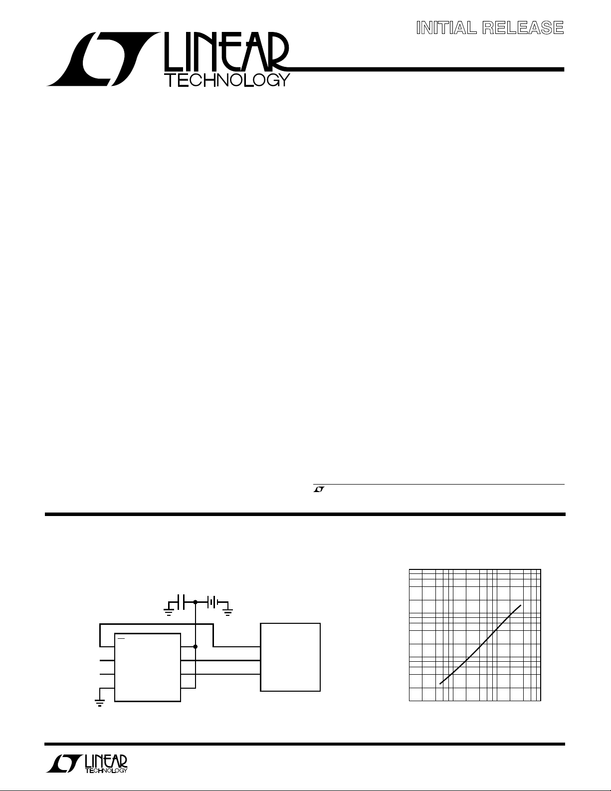
ANALOG INPUT
0V TO 3V RANGE
A
PPLICATITYPICAL
Samples at 200Hz and Runs Off a 3V Battery
1
CS/
SHDN
2
+IN
LTC1096L
3
–IN
4
GND
U
O
Supply Current vs Sample Rate10µW, SO-8 Package, 8-Bit A/D Converter
3V1µF
8
V
CC
7
CLK
6
D
OUT
V
REF
SERIAL DATA LINK
5
Information furnished by Linear Technology Corporation is believed to be accurate and reliable.
However, no responsibility is assumed for its use. Linear Technology Corporation makes no representation that the interconnection of its circuits as described herein will not infringe on existing patent rights.
MPU
SERIAL DATA LINK
(MICROWIRE AND
SPI COMPATIBLE)
1096/8 TA01
1
Page 2
LTC1096L/LTC1098L
TOP VIEW
+IN
–IN
GND
V
CC
CLK
D
OUT
V
REF
S8 PACKAGE
8-LEAD PLASTIC SO
CS/
SHDN
1
2
3
4
8
7
6
5
A
W
O
LUTEXI T
S
A
WUW
ARB
U
G
I
S
Supply Voltage (VCC) to GND................................... 12V
Voltage
Analog and Reference ................ –0.3V to V
CC
+ 0.3V
Digital Inputs......................................... –0.3V to 12V
Digital Outputs ........................... –0.3V to V
CC
+ 0.3V
Power Dissipation.............................................. 500mW
WU
/
PACKAGE
T
JMAX
Consult factory for Military grade parts.
O
RDER I FOR ATIO
= 150°C, θJA = 175°C/W
ORDER PART
NUMBER
LTC1096LACS8
LTC1096LAIS8
LTC1096LCS8
LTC1096LIS8
S8 PART MARKING
096LIA
1096LA
1096LI
1096L
(Notes 1 and 2)
Operating Temperature
LTC1096LAC/LTC1098LAC .................... 0°C to 70°C
LTC1096LAI/LTC1098LAI .................. –40°C to 85°C
LTC1096LC/LTC1098LC......................... 0°C to 70°C
LTC1096LI/LTC1098LI ....................... –40°C to 85°C
Storage Temperature Range ................. –65°c to 150°C
Lead Temperature (Soldering, 10 sec.)................ 300°C
U
(Note 3)
ORDER PART
NUMBER
LTC1098LACS8
LTC1098LAIS8
LTC1098LCS8
LTC1098LIS8
S8 PART MARKING
098LIA
1098LA
1098LI
1098L
CS/
SHDN
CH0
CH1
GND
T
JMAX
TOP VIEW
1
2
3
4
S8 PACKAGE
8-LEAD PLASTIC SO
= 150°C, θJA = 175°C/W
8
7
6
5
V
CC(VREF)
CLK
D
OUT
D
IN
WUW
UUU
RECO E DED OPERATI G CO DITIO S
SYMBOL PARAMETER CONDITIONS MIN TYP MAX UNITS
V
CC
f
CLK
t
CYC
t
hDI
t
suCS
t
WAKEUP
t
suDI
t
WHCLK
t
WLCLK
t
WHCS
t
WLCS
Supply Voltage 2.65 4.0 V
Clock Frequency VCC = 2.65V 25 250 kHz
Total Cycle Time LTC1096L, f
Hold Time, DIN After CLK↑ VCC = 2.65V 450 ns
Setup Time CS↓ Before First CLK↑ (See Operating Sequence) VCC = 2.65V, LTC1096L 1 µs
Wakeup Time CS↓ Before First CLK↓ After First CLK↑ VCC = 2.65V, LTC1096L 10 µs
(See Figure 1, LTC1096L Operating Sequence)
Wakeup Time CS↓ Before MSBF Bit CLK↓ VCC = 2.65V, LTC1098L 10 µs
(See Figure 2, LTC1098L Operating Sequence)
Setup Time, DIN Stable Before CLK↑ VCC = 2.65V 1 µs
CLK High Time VCC = 2.65V 1.6 µs
CLK Low Time VCC = 2.65V 1.6 µs
CS High Time Between Data Transfer Cycles VCC = 2.65V 2 µs
CS Low Time During Data Transfer LTC1096L, f
LTC1098L, f
VCC = 2.65V, LTC1098L 1 µs
LTC1098L, f
= 250kHz 58 µs
CLK
= 250kHz 58 µs
CLK
= 250kHz 56 µs
CLK
= 250kHz 56 µs
CLK
2
Page 3
LTC1096L/LTC1098L
UU W
CO VERTER A D ULTIPLEXER CHARACTERISTICS
V
= 2.65V, V
CC
= 2.5V, f
REF
= 250kHz, unless otherwise noted.
CLK
PARAMETER CONDITIONS MIN TYP MAX MIN TYP MAX UNITS
Resolution (No Missing Code) ● 8 8 Bits
Offset Error (Note 4) ● ±0.5 ±1 LSB
Linearity Error ● ±0.5 ±1 LSB
Full Scale Error ● ±0.5 ±1 LSB
Total Unadjusted Error (Note 5) V
Analog Input Range (Note 6) V
REF Input Range (Note 6) 2.65 ≤ VCC ≤ 4.0V V
Analog Input Leakage Current (Note 7) ● ±1 ±1 µA
= 2.5V ● ±1 ±1.5 LSB
REF
LTC1096LA/LTC1098LA
–0.05V to V
–0.05V to V
LTC1096L/LTC1098L
+ 0.05V
CC
+ 0.05V
CC
U
D
DIGITAL
VCC = 2.65V, V
SYMBOL PARAMETER CONDITIONS MIN TYP MAX UNITS
V
IH
V
IL
I
IH
I
IL
V
OH
V
OL
I
OZ
I
SOURCE
I
SINK
I
REF
I
CC
A
= 2.5V, f
REF
High Level Input Voltage VCC = 3.6V ● 1.9 V
Low Level Input Voltage VCC = 2.65V ● 0.45 V
High Level Input Current VIN = V
Low Level Input Current VIN = 0V ● –2.5 µA
High Level Output Voltage VCC = 2.65V, IO = 10µA ● 2.4 2.64 V
Low Level Output Voltage VCC = 2.65V, IO = 400µA ● 0.3 V
Hi-Z Output Leakage CS =High ● ±3 µA
Output Source Current V
Output Sink Current V
Reference Current CS = V
Supply Current CS = V
DC
CLK
LECTRICAL C CHARA TER ST
E
= 250kHz, unless otherwise noted.
CC
I
= 0V –10 mA
OUT
= V
OUT
≥ 200µs, f
t
CYC
= 58µs, f
t
CYC
LTC1096L, t
LTC1098L, t
= 360µA ● 2.1 2.50 V
O
CC
CC
CC
≤ 50kHz ● 3.500 7.5 µA
CLK
= 250kHz ● 35.00 50.0 µA
CLK
≥ 200µs, f
CYC
= 58µs, f
t
CYC
≥ 200µs, f
CYC
= 58µs, f
t
CYC
ICS
I
● 2.5 µA
15 mA
● 0.001 2.5 µA
● 0.001 ± 3 µA
≤ 50kHz ● 40 80 µA
CLK
= 250kHz ● 120 180 µA
CLK
≤ 50kHz ● 44 88 µA
CLK
= 250kHz ● 155 230 µA
CLK
3
Page 4

LTC1096L/LTC1098L
AC CHARACTERISTICS
VCC = 2.65V, V
SYMBOL PARAMETER CONDITIONS MIN TYP MAX UNITS
t
SMPL
f
SMPL
(MAX)
t
CONV
t
dDO
t
dis
t
en
t
hDO
t
f
t
r
C
IN
= 2.5V, f
REF
Analog Input Sample Time See Operating Sequences 1.5 CLK Cycles
Maximum Sampling Frequency ● 16.5 kHz
Conversion Time See Operating Sequences 8 CLK Cycles
Delay Time, CLK↓ to D
Delay Time, CS↑ to D
Delay Time, CLK↓ to D
Time Output Data Remains Valid After CLK↓ C
D
Fall Time See Test Circuits ● 70 250 ns
OUT
D
Rise Time See Test Circuits ● 50 200 ns
OUT
Input Capacitance Analog Inputs On Channel 25 pF
= 250kHz, unless otherwise noted.
CLK
Data Valid See Test Circuits ● 500 1000 ns
OUT
Hi-Z See Test Circuits ● 220 800 ns
OUT
Enable See Test Circuits ● 160 480 ns
OUT
= 100pF 400 ns
LOAD
Off Channel 5 pF
Digital Input 5 pF
The ● denotes specifications which apply over the full operating
temperature range.
Note 1: Absolute Maximum Ratings are those values beyond which the life
of a device may be impaired.
Note 2: All voltage values are with respect to GND.
Note 3: This device is specified at 2.65V. Consult factory for 5V specified
devices.
Note 4: Linearity error is specified between the actual end points of the
A/D transfer curve.
Note 5: Total unadjusted error includes offset, full scale, linearity,
multiplexer and hold step errors.
U
UU
PI FU CTIO S
LTC1096L
CS/SHDN (Pin 1): Chip Select Input. A logic low on this
input enables the LTC1096L. A logic high on this input
disables the LTC1096L and disconnects the power to the
LTC1096L.
IN+ (Pin 2): Analog Input. This input must be free of noise
with respect to GND.
IN– (Pin 3): Analog Input. This input must be free of noise
with respect to GND.
GND (Pin 4): Analog Ground. GND should be tied directly
to an analog ground plane.
V
(Pin 5): Reference Input. The reference input defines
REF
the span of the A/D converter and must be kept free of
noise with respect to GND.
Note 6: Two on-chip diodes are tied to each reference and analog input
which will conduct for reference or analog input voltages one diode drop
below GND or one diode drop above VCC. This spec allows 50mV forward
bias of either diode for 2.65V ≤ VCC ≤ 3.6V. This means that as long as the
reference or analog input does not exceed the supply voltage by more than
50mV, the output code will be correct. To achieve an absolute 0V to 3V
input voltage range will therefore require a minimum supply voltage of
2.950V over initial tolerance, temperature variations and loading.
Note 7: Channel leakage current is measured after the channel selection.
D
(Pin 6): Digital Data Output. The A/D conversion
OUT
result is shifted out of this output.
CLK (Pin 7): Shift Clock. This clock synchronizes the serial
data transfer.
V
(Pin 8): Power Supply Voltage. This pin provides
CC
power to the A/D converter. It must be free of noise and
ripple by bypassing directly to the analog ground plane.
LTC1098L
CS/SHDN (Pin 1): Chip Select Input. A logic low on this
input enables the LTC1098L. A logic high on this input
disables the LTC1098L and disconnects the power to the
LTC1098L.
CHO (Pin 2): Analog Input. This input must be free of noise
with respect to GND.
4
Page 5

LTC1096L/LTC1098L
U
UU
PI FU CTIO S
CH1 (Pin 3): Analog Input. This input must be free of noise
with respect to GND.
GND (Pin 4): Analog Ground. GND should be tied directly
to an analog ground plane.
DIN (Pin 5): Digital Data Input. The multiplexer address is
shifted into this pin.
TEST CIRCUITS
Load Circuit for t
D
OUT
1.4V
dDO
3k
100pF
, tr and t
TEST POINT
f
LTC1096/98 • TC01
D
(Pin 6): Digital Data Output. The A/D conversion
OUT
result is shifted out of this output.
CLK (Pin 7): Shift Clock. This clock synchronizes the serial
data transfer.
VCC (V
(Pin 8): Power Supply Voltage. This pin pro-
REF)
vides power and defines the span of the A/D converter. It
must be free of noise and ripple by bypassing directly to
the analog ground plane
Voltage Waveforms for D
D
OUT
t
r
Rise and Fall Times, tr, t
OUT
t
f
V
OH
V
OL
LTC1096/98 • TC02
f
Load Circuit for t
TEST POINT
D
OUT
3k
100pF
and t
dis
en
VCC t
WAVEFORM 2, t
dis
t
WAVEFORM 1
dis
LTC1096/98 • TC03
Voltage Waveforms for D
CLK
D
OUT
Voltage Waveforms for t
CS
D
OUT
en
V
IL
t
dDO
WAVEFORM 1
(SEE NOTE 1)
D
OUT
WAVEFORM 2
(SEE NOTE 2)
NOTE 1: WAVEFORM 1 IS FOR AN OUTPUT WITH INTERNAL CONDITIONS SUCH
THAT THE OUTPUT IS HIGH UNLESS DISABLED BY THE OUTPUT CONTROL.
NOTE 2: WAVEFORM 2 IS FOR AN OUTPUT WITH INTERNAL CONDITIONS SUCH
THAT THE OUTPUT IS LOW UNLESS DISABLED BY THE OUTPUT CONTROL.
Delay Time, t
OUT
dDO
V
OH
V
OL
LTC1096/98 • TC05
dis
V
IH
90%
t
dis
10%
LTC1096/98 • TC04
5
Page 6

LTC1096L/LTC1098L
TEST CIRCUITS
D
D
CLK
CS
CLK
OUT
CS
IN
LTC1096L
LTC1098L
Voltage Waveforms for t
t
WAKEUP
START
12345
en
1
t
en
B7
V
OL
LTC1096/98 • TC06
D
OUT
PPLICATI
A
U
O
S
I FOR ATIO
WU
U
INPUT DATA WORD
The LTC1096L requires no DIN word. It is permanently
configured to have a single differential input. The conversion result, in which the output on the D
OUT
line is
presented in MSB-first sequence followed by LSB sequence, provides easy interface to MSB- or LSB-first
serial ports.
The LTC1098L latches data into the DIN input on the rising
edge of the clock. The input data words are defined as
follows:
SGL/
ODD/
SIGN
MSB-FIRST/
MSBFSTART
LSB-FIRST
LTC1096/9 • AI01
DIFF
MUX
ADDRESS
B7
V
OL
t
en
LTC1096/98 • TC07
Start Bit
The first “logical one” clocked into the DIN input after CS
goes low is the start bit. The start bit initiates the data
transfer. The LTC1098L will ignore all leading zeroes
which precede this logical one. After the start bit is
received, the remaining bits of the input word will be
clocked in. Further inputs on the DIN pin are then ignored
until the next CS cycle.
Multiplexer (MUX) Address
The bits of the input word following the START bit assign
the MUX configuration for the requested conversion. For
a given channel selection, the converter will measure the
voltage between the two channels indicated by the “+” and
“–” signs in the selected row of the following tables. In
6
Page 7

LTC1096L/LTC1098L
PPLICATI
A
U
O
S
I FOR ATIO
WU
U
single-ended mode, all input channels are measured with
respect to GND.
LTC1098L Channel Selection
MUX ADDRESS
SGL/DIFF
1
1
0
0
ODD/SIGN
0
1
0
1
CHANNEL #
CH0
+
+
–
CH1
+
–
+
LTC1096/8 • AI02
GND
–
–
MSB-First/LSB-First (MSBF)
The output data of the LTC1098L is programmed for
MSB-first or LSB-first sequence using the MSBF bit.
When the MSBF bit is a logical one, data will appear on
the D
line in MSB-first format. Logical zeroes will be
OUT
filled in indefinitely following the last data bit. When the
MSBF bit is a logical zero, LSB-first data will follow the
normal MSB-first data on the D
line (see Figures 1
OUT
and 2).
ANALOG CONSIDERATIONS
Grounding
The LTC1096L/LTC1098L should be used with an analog
ground plane and single point grounding techniques. Do
not use wire wrapping techniques to breadboard and
evaluate the device. To achieve the optimum performance
use a printed circuit board. The GND pin (Pin 4) should be
tied directly to the ground plane with minimum lead
length.
Bypassing
For good performance, the LTC1096L/LTC1098L VCC and
V
pins must be free of noise and ripple. Any changes in
REF
the VCC and V
voltage with respect to ground during the
REF
conversion cycle can induce errors or noise in the output
code. Bypass the VCC and V
pins directly to the analog
REF
ground plane with a minimum 0.1µF capacitor and with
leads as short as possible. The LTC1098L combines V
and V
into one pin, VCC(V
REF
), which can be bypassed
REF
CC
by a 0.1µF capacitor.
Analog Inputs
Because of the capacitive redistribution A/D conversion
techniques used, the analog inputs of the LTC1096L/
LTC1098L have capacitive switching input current spikes.
These current spikes settle quickly and do not cause a
problem. But if large source resistances are used or if slow
settling op amps drive the inputs, take care to ensure the
transients caused by the current spikes settle completely
before the conversion begins.
D
CLK
OUT
t
CYC
CS
t
Hi-Z
suCS
t
WAKEUP
NULL
BIT
B3B4B5
B7
B6
t
CONV
Figure 1. LTC1096L Operating Sequence
B2
B0
B1
B2B1
B3
B4
B7B6B5
FILLED
WITH
ZEROES
POWER
DOWN
Hi-Z
LTC1096/98 F01
7
Page 8

LTC1096L/LTC1098L
U
O
PPLICATI
A
MSB-FIRST DATA (MSBF = 0)
CS
CLK
t
suCS
D
IN
D
OUT
START
Hi-Z
t
WAKEUP
SGL/
DIFF
t
SMPL
S
I FOR ATIO
ODD/
SIGN
MSBF
NULL
B7
BIT
Figure 2. LTC1098L Operating Sequence Example: Differential Inputs (CH+, CH–)
PACKAGE DESCRIPTION
WU
B6
t
CONV
U
t
CYC
B3B4B5
B2
DON'T CARE
B0
B1
B2B1
B3
B4
U
Dimensions in inches (millimeters) unless otherwise noted.
B7B6B5
FILLED
WITH
ZEROES
POWER
DOWN
Hi-Z
LTC1096/98 F02
S8 Package
8-Lead Plastic Small Outline (Narrow 0.150)
(LTC DWG # 05-08-1610)
0.189 – 0.197*
(4.801 – 5.004)
7
8
0.010 – 0.020
(0.254 – 0.508)
0.008 – 0.010
(0.203 – 0.254)
*
DIMENSION DOES NOT INCLUDE MOLD FLASH. MOLD FLASH
SHALL NOT EXCEED 0.006" (0.152mm) PER SIDE
**
DIMENSION DOES NOT INCLUDE INTERLEAD FLASH. INTERLEAD
FLASH SHALL NOT EXCEED 0.010" (0.254mm) PER SIDE
× 45°
0.016 – 0.050
0.406 – 1.270
0°– 8° TYP
0.053 – 0.069
(1.346 – 1.752)
0.014 – 0.019
(0.355 – 0.483)
(0.101 – 0.254)
0.050
(1.270)
BSC
0.004 – 0.010
0.228 – 0.244
(5.791 – 6.197)
1
2
RELATED PARTS
PART NUMBER DESCRIPTION COMMENTS
LTC1096/LTC1098 8-Pin SO, Micropower 8-Bit ADC Low Power, Small Size, Low Cost
LTC1196/LTC1198 8-Pin SO, 1Msps 8-Bit ADC Low Power, Small Size, Low Cost
LTC1285/LTC1288 8-Pin SO, 3V Micropower 12-Bit ADC 12-Bit ADC in SO-8
LTC1289 Multiplexed 3V 12-Bit ADC 8-Channel 12-Bit Serial I/O
LTC1584L Multiplexed 3V 12-Bit ADC 4-Channel 12-Bit Serial I/O, Micropower
5
6
0.150 – 0.157**
(3.810 – 3.988)
3
4
SO8 0695
8
Linear Technology Corporation
1630 McCarthy Blvd., Milpitas, CA 95035-7417
(408) 432-1900
●
FAX
: (408) 434-0507
●
TELEX
: 499-3977
LT/GP 1295 5K REV A • PRINTED IN USA
LINEAR TE CHNOLO GY CORPOR ATION 1995
 Loading...