

Page 1

COLOR TFT-LCD TV
SERVICE MANUAL
MODEL : LT-40FLP
CAUTION !!
BEFORE SERVICING THE TFT-LCD TV,
READ THE SAFETY PRECAUTIONS IN THIS MANUAL.
SERVICE MANUAL
PAGE:1
Page 2
SAFETY PRECAUTIONS
!! Important Safety Notice !!
Many electrical and mechanical parts in this chassis have special safety-related
characteristics.
These parts are identified by in the Schematic Diagram and Replacement Parts List.
It is essential that these special safety parts should be replaced with the same components
as recommended in this manual to prevent Shock, Fire, or other Hazards.
Do not modify the original design without permission of manufacturer.
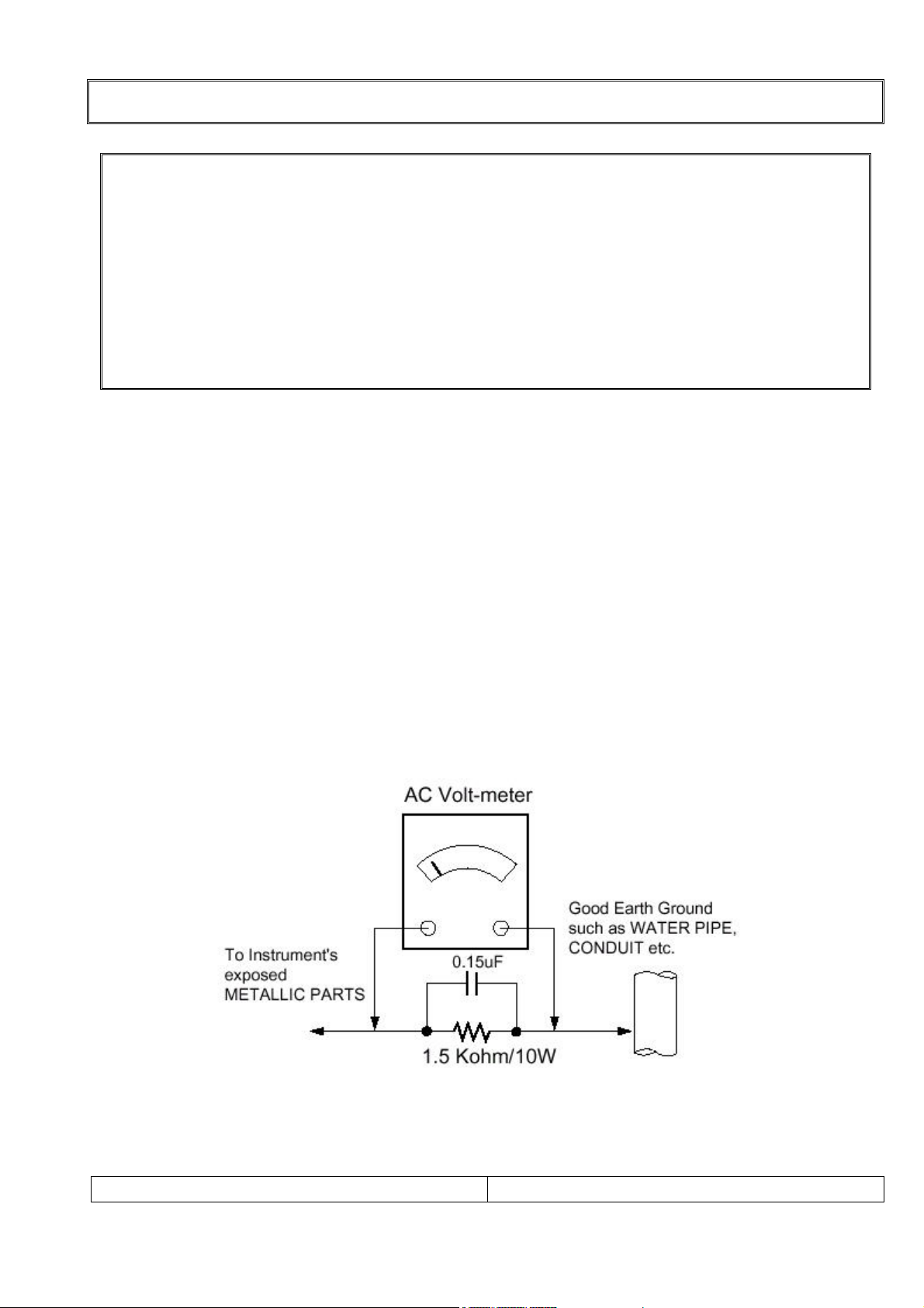
Leakage Current Hot Check (See below Figure)
Plug the AC cord directly into the AC outlet.
Do not use a line Isolation Transformer during this check.
Connect 1.5K/10watt resistor in parallel with a 0.15uF capacitor between a known good earth
ground (Water Pipe, Conduit, etc.) and the exposed metallic parts.
Measure the AC voltage across the resistor using AC voltmeter with 1000 ohms/volt or more
sensitivity.
Reverse plug of the AC cord into the AC outlet and repeat AC voltage measurements for each
exposed metallic part. Any voltage measured must not exceed 0.75 volt RMS, which is,
corresponds to 0.5mA.
In case any measurement is out of the limits specified, there is possibility of shock hazard and
the set must be checked and repaired before it is returned to the customer.
Leakage Current Hot Check circuit
SERVICE MANUAL
PAGE:2
Page 3

SERVICING PRECAUTIONS
CAUTION!!
Before servicing receivers covered by this service manual, read and follow the SAFETY
PRECAUTIONS on page 2 of this publication.
General Servicing Precautions
1.Always unplug the receiver AC power cord from AC power source before;
ⓐRemoving or reinstalling any component, circuit board module or any other receiver assembly.
ⓑDisconnecting or reconnecting any receiver electrical plug or other electrical connection.
ⓒConnecting a test substitute in parallel with an electrolytic capacitor in the receiver.
CAUTION!! A wrong part substitution or incorrect polarity installation of electrolytic capacitors
may result in an explosion harzard.
2.Do not spray chemicals on or near this receiver or any of its assemblies.
3.Do not defect any plug/socket voltage interlocks with which receivers covered by this service
manual might be equipped.
4.Always connect the test receiver ground lead to the receiver chassis ground before
connecting the test receiver positive lead. Always remove the test receiver ground lead last.
5.Do not connect the test fixture ground strap to power supply heatsink in this receiver
Electrostatically Sensitive(ES) Devices
Some semiconductor(solid state) devices can be damaged easily by static electricity. Such
components commonly are called Electrostatically Sensitive(ES) Device.Examples
Circuit Board Foil Repair
Excessive heat applied to the copper foil of any printed circuit board will weaken the adhesive
that bonds the foil to the circuit board causing the foil th separate from or “lift-off” the board.
The following guidelines and procedures should be flollowed whenever this condition is
encountered.
At IC Connections
To repair a defective copper pattern at IC connections use the following procedure to install a
jumper wire on the copper pattern side of the circuit board.(Use this technique only on IC
connections.)
1.Carefully remove the damaged copper pattern with a sharp knife.(Remove only as much
copper as absolutely necessary.)
2.Carefully scratch away the solder resist and acrylic coating(if used) from the end of the
remaining coopper pattern.
3.Bend a small “U” in one end of a small guage jumper wire and carefully crimp it around the IC
pin.
4.Route the jumper wire along the path of the out-away copper pattern and let it overlap the
previously scraped end of the good copper pattern. Solder the overlapped area and clip off any
excess jumper wire.
SERVICE MANUAL
PAGE:3
Page 4

CONTENTS
Safety precautions ----------------------------------------------------------- 2
Servicing precautions ------------------------------------------------------- 3
Contents ------------------------------------------------------------------------- 4
Specifications ----------------------------------------------------------------- 5
Location of control ---------------------------------------------------------- 9
Deassembly procedure ---------------------------------------------------- 12
Mechanical exploded view with part list ----------------------------- 19
Circuit descriptions --------------------------------------------------------- 21
Trouble shooting ------------------------------------------------------------- 58
Wire dressing ----------------------------------------------------------------- 63
Adjustment instruction with SVC mode ------------------------------ 65
Inspection instruction ------------------------------------------------------ 69
PCB Layout --------------------------------------------------------------------- 71
Part appearance -------------------------------------------------------------- 76
Replacement part list -------------------------------------------------------- 79
Block diagram ---------------------------------------------------------------- 90
Connection diagram -------------------------------------------------------- 91
Schemetic diagram --------------------------------------------------------- 92
Wave form --------------------------------------------------------------------- 93
SERVICE MANUAL
PAGE:4
Page 5

SPECIFICATIONS
Note: Specifications and others are subject to change without notice for improvement.
1.Scope.
This document is the specification of 40” TFT-LCD Color TV.
2.Power
1) Power requirement
275W
2) AC / DC SMPS Adapter.
Input Frequency : 50/60㎐
Input Voltage: AC 100V ~ AC 240V (±10%)
Output Voltage: DC 5V,12V, 30V,
3) Power cord
Use UL listed and CSA certified detachable power cord type; SVT, 3-conductors, 18AWG
For AC 120V area. Use VDE listed detachable power cord type; HO5VV-F, 3-conductors,
18AWG for AC 220~240V area.
3.Tuning system
FVS 100 Program
4.Sound output
10W+10Wrms Stereo (Max)
5.Antenna input impedance
VHF / UHF at 75ohm
6.OSD Type (On Screen Display)
Windows type (Center)
7.External in/output
DVI-INPUT,S-VIDEO INPUT,HEADPHONE OUTPUT,ANALOG PC INPUT,PC AUDIO INPUT,
SCART 2 INPUT ,SUB WOOFER OUTPUT,ANTENNA INPUT
8. Function
CATV/Hyper band
Auto Program
Manual Program
Auto Sleep
Quick view
ACMS(Auto channel Memory System)
PSM(Picture Status memory)
SSM(Sound Status memory)
PIP(PICTURE IN RICTURE)
ARC(ASPECT RATIO CONTROL)
SERVICE MANUAL
PAGE:5
Page 6
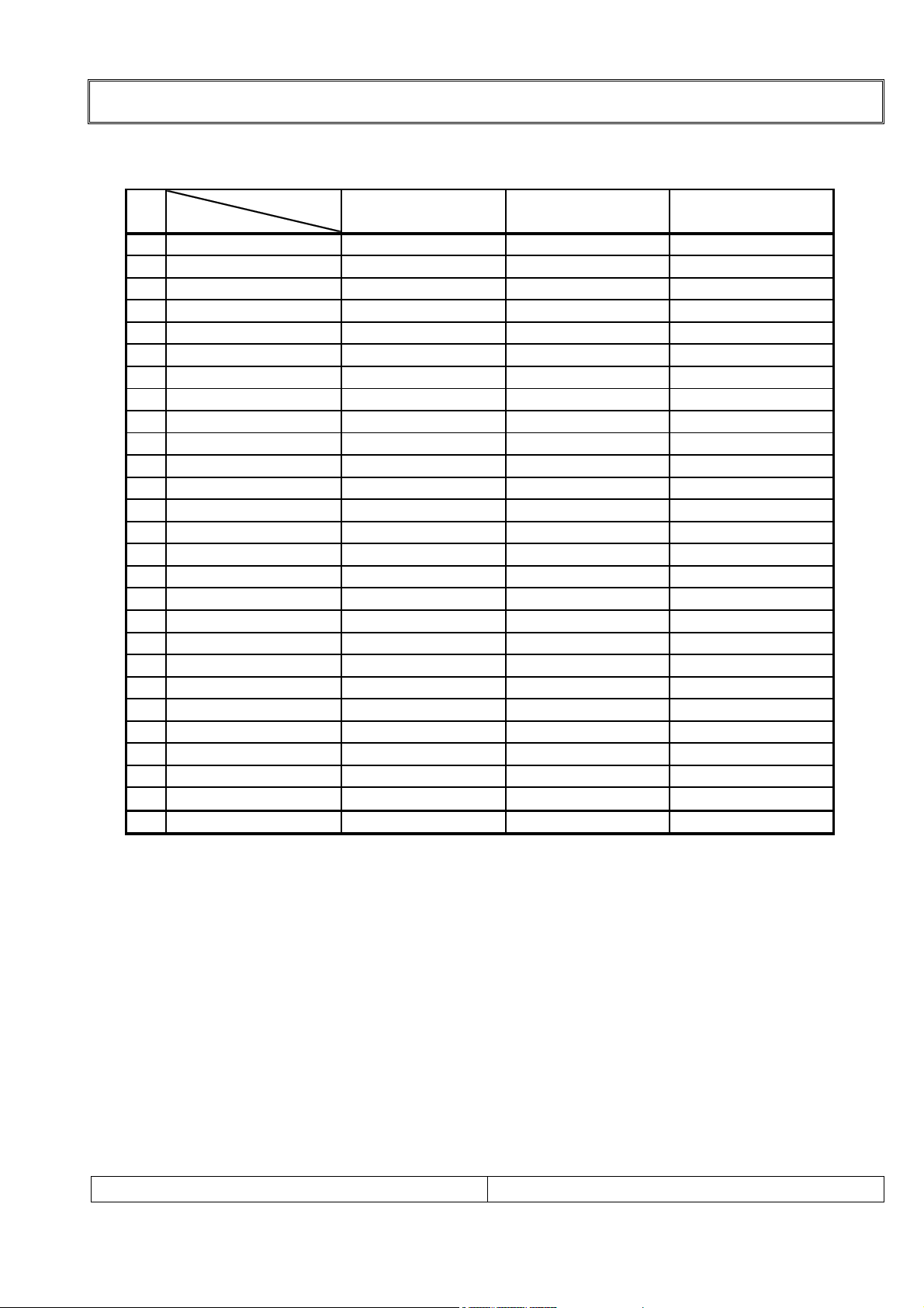
9.Receiving RF TV system
NO
Model System
1 PAL-B
2 PAL-G
3 PAL-I, I /I
4 PAL-D
5 PAL-K
6 SECAM-B
7 SECAM-G
8 SECAM-D
9 SECAM-K
10 SECAM-K1
11 SECAM-I (6.0)
12 NTSC-3.58 / 4.5
13 NTSC-3.58 / 5.5
14 NTSC-3.58 / 6.0
15 NTSC-3.58 / 6.5
16 NTSC-3.58 / 4.5(5.0)
17 NTSC-4.43 / 5.5
18 NTSC-4.43 / 6.0
19 NTSC-4.43 / 6.5
20 PAL 5.5 / 60Hz
21 PAL 6.0 / 60Hz
22 PAL 6.5 / 60Hz
23 SECAM 5.5 / 60Hz
24 SECAM 6.0 / 60Hz
25 SECAM 6.5 / 60Hz
26 SECAM L / L' X
TOTAL SYSTEM 25
SPECIFICATIONS
40FLP / /
○/ /
○/ /
○/ /
○/ /
○/ /
○/ /
○/ /
○/ /
○/ /
○/ /
○/ /
○/ /
○/ /
○/ /
○/ /
○/ /
○/ /
○/ /
○/ /
○/ /
○/ /
○/ /
○/ /
○/ /
○/ /
//
//
SERVICE MANUAL
PAGE:6
Page 7
SPECIFICATIONS
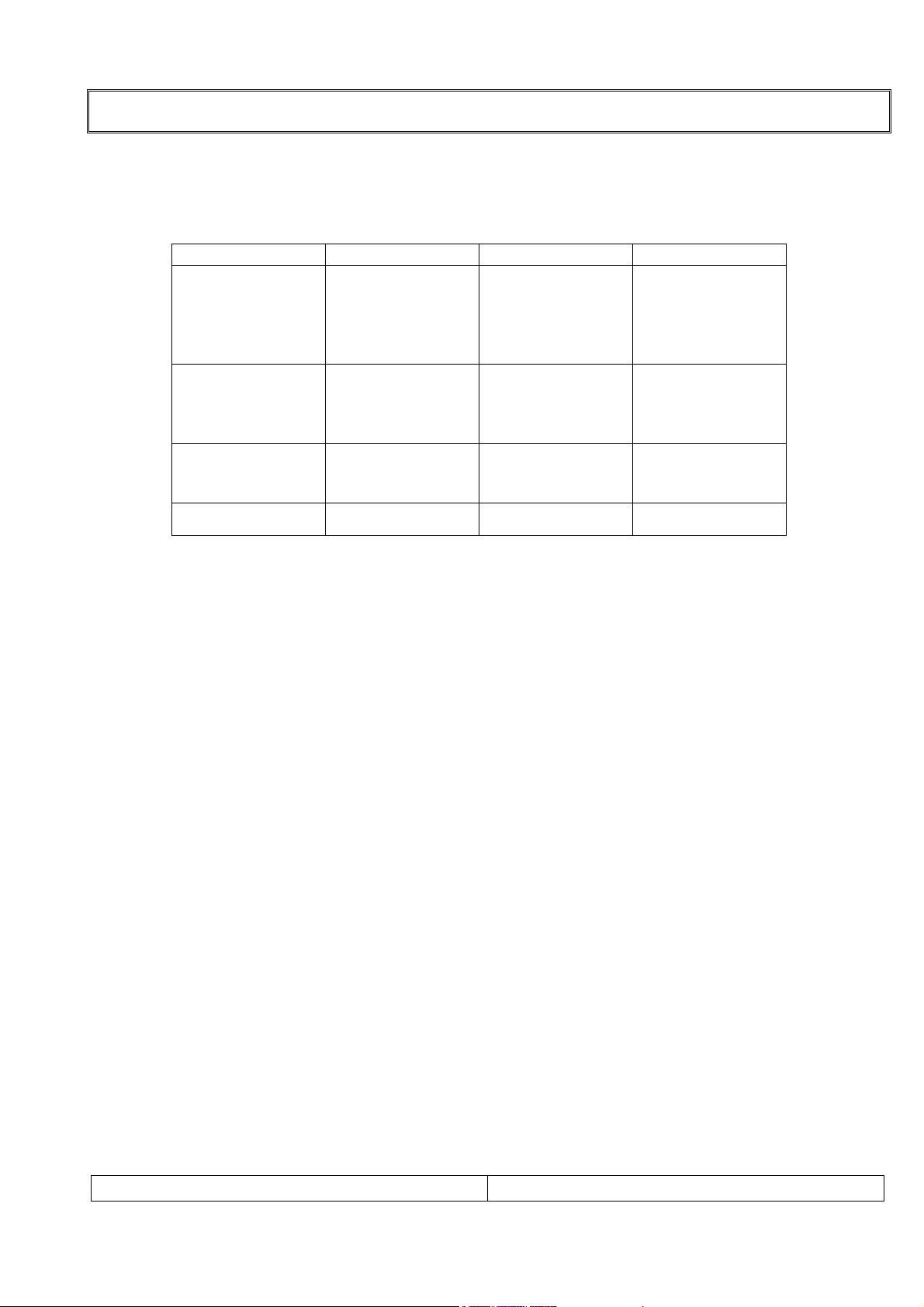
11. PC Mode Scan Frequency & Timing
1) Scan Freq: H: 15 ~ 110 kHz / V: 56 ~ 75㎐
2) Preset Timing Chart
Mode Resolution H-Freq(KHz) V-Freq(KHz)
31.5KHz
37.9KHz
37.5KHz
31.5KHz
35.1KHz
37.9KHz
48.1KHz
46.9KHz
48.4KHz
56.5KHz
60.2KHz
VGA
SVGA
XGA
640x480
640x480
640x480
640x480
720x400
800x600
800x600
800x600
800x600
1024x768
1024x768
1024x768
35 KHz
60Hz
67Hz
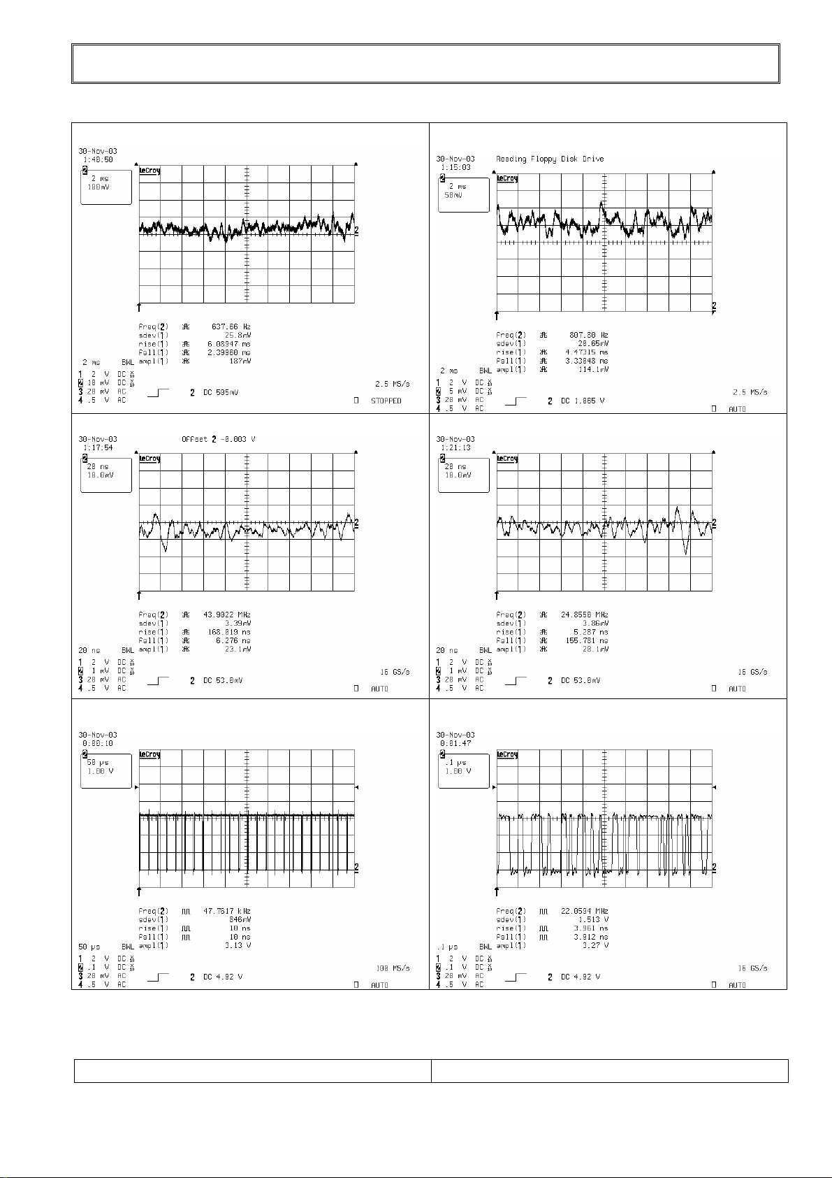
72Hz
75Hz
70Hz
56Hz
60Hz
72Hz
75Hz
60Hz
70Hz
75Hz
WXGA
1280x768 47.7KHZ 60Hz
Note!! :
ⓐ If the set is cold, there may be a small “flicker” when the set is switched on. This is
Normal, there is nothing wrong with the set.
ⓑ if possible, use the VESA 1024 x 768@60HZ video mode to obtain the best image
quality for your LCD monitor. If used under the other resolutions, some scaled or processed
pictures may appear on the screen.
ⓒ some dot defects may appear on the screen, like Red, Green or Blue spot.
However, this will have no impact or effect on the monitor performance.
SERVICE MANUAL
PAGE:7
Page 8

SPECIFICATIONS
13. TFT – LCD Panel Character
1) Feature
Size : 40 inches diagonal
LCD Type : a-si TFT Active MatriX
Pixel Pitch : 0.681mm (V) x 0.681mm(H) x RGB
Pixel Format : 1280 horiz. By 768 vert. Pixels RGB strip arrangement
Active Video Area : 871.68mm (H) x 523.008 mm (V)
Surface treatment : Haze 44% , Hard coating (3H)
Response Time (Typ) : Tr : 15 ms Tf : 8 ms
Viewing Angle<CR≥10> : Hor [Left/Right] Æ 85Deg (Typ) / 85Deg (Typ),
Ver [High (Top)/Low (Bottom)] Æ 85Deg (Typ) / 85Deg (Typ)
Luminance(Typ) : 450 cd/㎡(Typ)
Contrast Ratio (Typ) : 600(Typ)
Display Color : 16.7M Color
Back Light : 20 CCFL
SERVICE MANUAL
PAGE:8
Page 9
LOCATION OF CONTROL
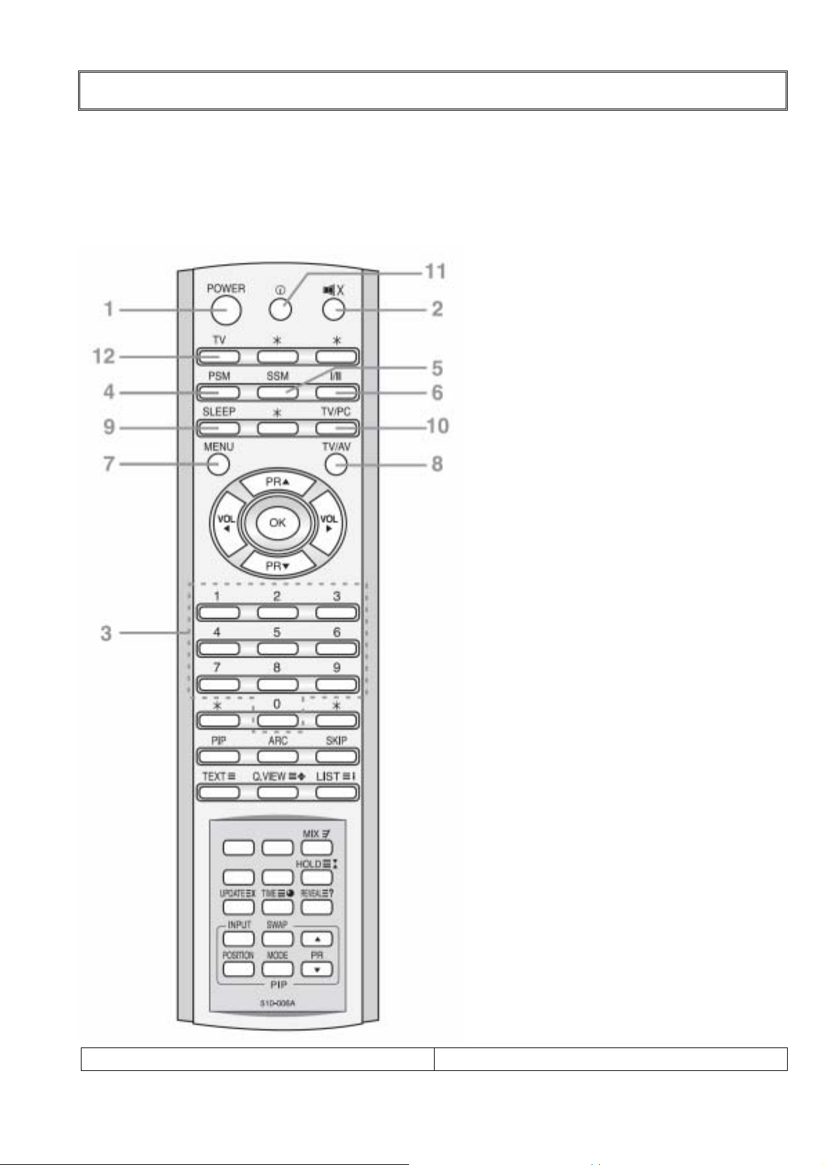
All the function can be controlled with the remote controller.
Some functions can also adjusted with the buttons on the controls on the TV front panel.
1-1. Remote controller
Note !! : Before you use the remote controller, please install the batteries.
1.POWER:
Turns the TV on from standby or off to
standby mode.
2.MUTE:
Turns the sound on and off
3.NUMBER buttons:
Select channel numbers.
4.PSM (Picture Status Memory):
Recalls your preferred picture setting.
5.SSM (Sound Status Memory):
Recalls your preferred sound setting.
6. I / II:
Selects the language during dual
language broadcast. / Selects the
sound output.
7.MENU:
Displays a main menu.
8.TV / AV:
Selects input signal source.
/ Clears the menu from the screen.
9.SLEEP:
Sets the sleep timer.
10.TV / PC :
Selects TV or PC mode directly.
11.Information Display
Use to see information on the current
boardcast
12. TV
The future reserved
SERVICE MANUAL
PAGE:9
Page 10
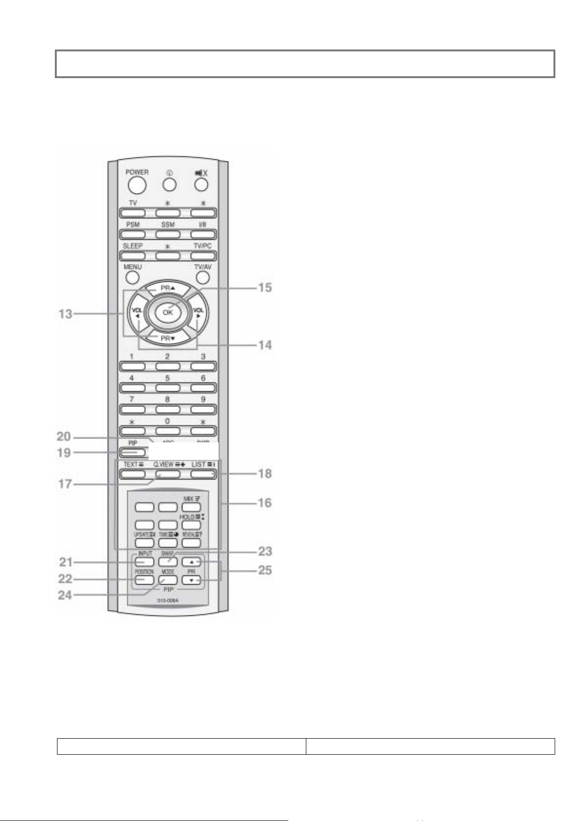
LOCATION OF CONTROL
1-2. Remote controller
Note !! : Before you use the remote controller, please install the batteries.
13.PR ▲▼ ( Programme Up/Down):
Selects a next programme or a menu item.
14.VOL ◀▶ ( Volume Up/Down):
Adjusts the sound level or a menu Setting.
15.OK
Accepts your selection or displays the current mode.
16. TELETEXT Buttons:
These buttons are used for TELETEXT. For further
details, see the TELETEXT Selection
17. Q.VIEW
Returns to the previously viewed Programme
Note: TELETEXT mode.
The Q.VIEW button is used for TELETEXT function.
18. LIST
Displays the program list menu.
19. PIP
Display a PIP (Picture In Picture) screen.
20. ARC
Selects a screen mode – 16:9, 14:9, ZOOM, 1:1 and
auto Wide.
21. INPUT
Selects the AV source of sub picture in PIP mode.
22. POSITION
Selects a position of PIP screen.
23. SWAP
Switches a main picture for sub picture in PIP mode.
24. MODE
Selects a PIP screen mode – 16:1,9:1,double window
and scan mode
25.▲PR▼
Selects a programme when RF signal is displayed in
PIP mode.
.
SERVICE MANUAL
PAGE:
10
Page 11
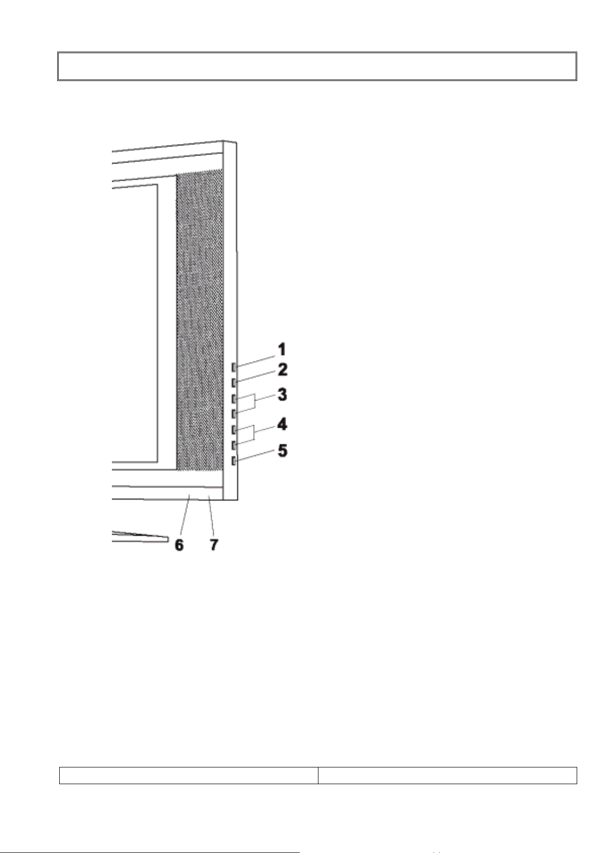
Controller of Panel
< SIDE VIEW>
SERVICE MANUAL
LOCATION OF CONTROL
1.ON/OFF:
Switches TV set on or off.
2.MENU:
Display a menu.
3.+ PR - ( Programme Up/Down):
Selects a programme or a menu item.
4.+ VOL -( Volume Up/Down):
Adjusts the volume.
Adjusts menu settings.
5.TV/AV:
Selects input signal source.
Clears the menu from the screen.
6:POWER INDICATOR:
Illuminates red when the TV is inpower standby mode.
Illuminates green when the TV isswitched power on mode.
Illuminates amber when the TV isswitched power saving mode.
7.REMOTE CONTROL SENSOR:
Accepts the IR signal of remote
controller.
PAGE:
11
Page 12
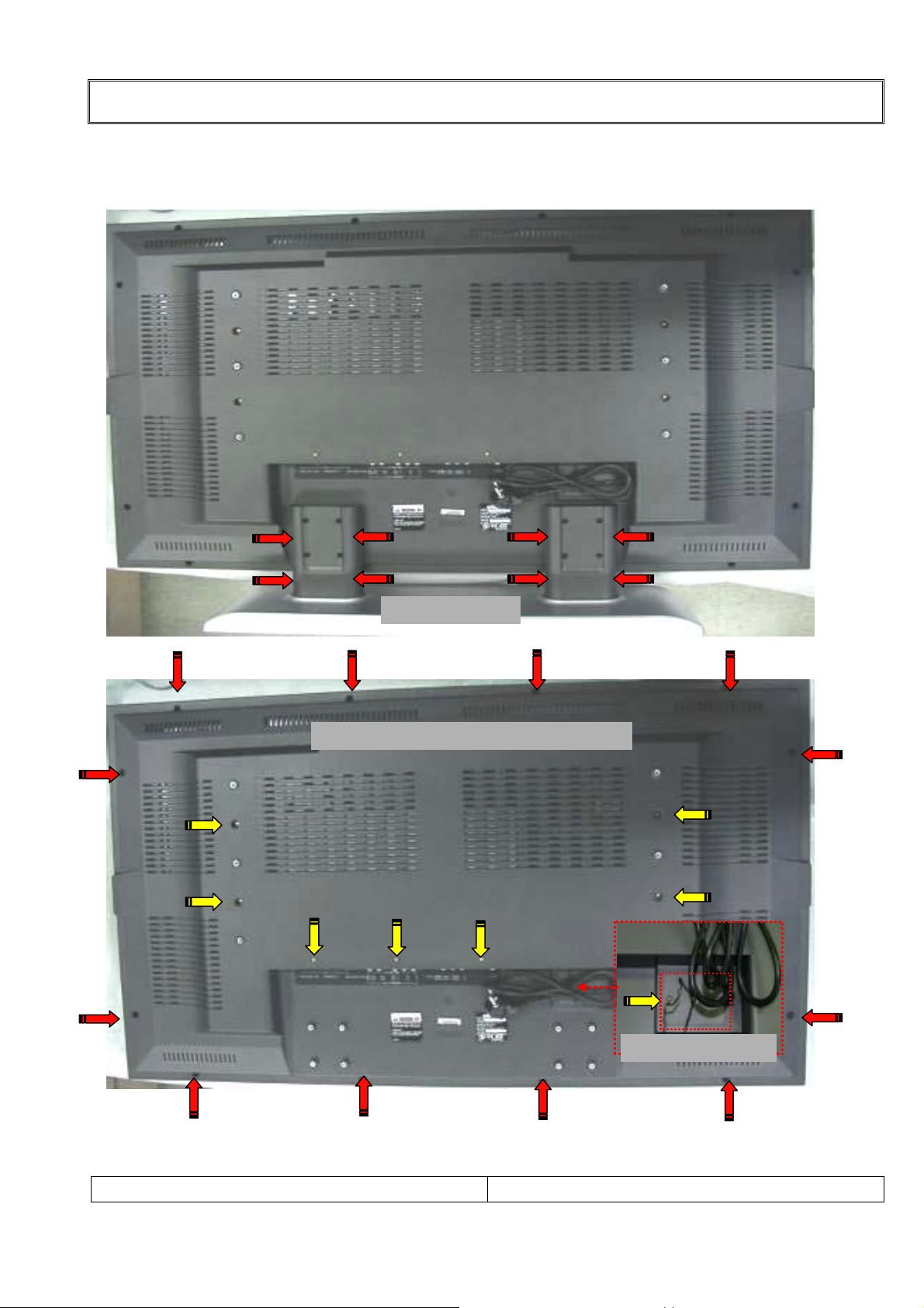
1. Disassembly procedure
1).Back cover
DISASSEMBLY PROCEDURE
Remove 8 Screw
Remove 20 Screw & Power cord holder
Power cord holder
SERVICE MANUAL
PAGE:
12
Page 13
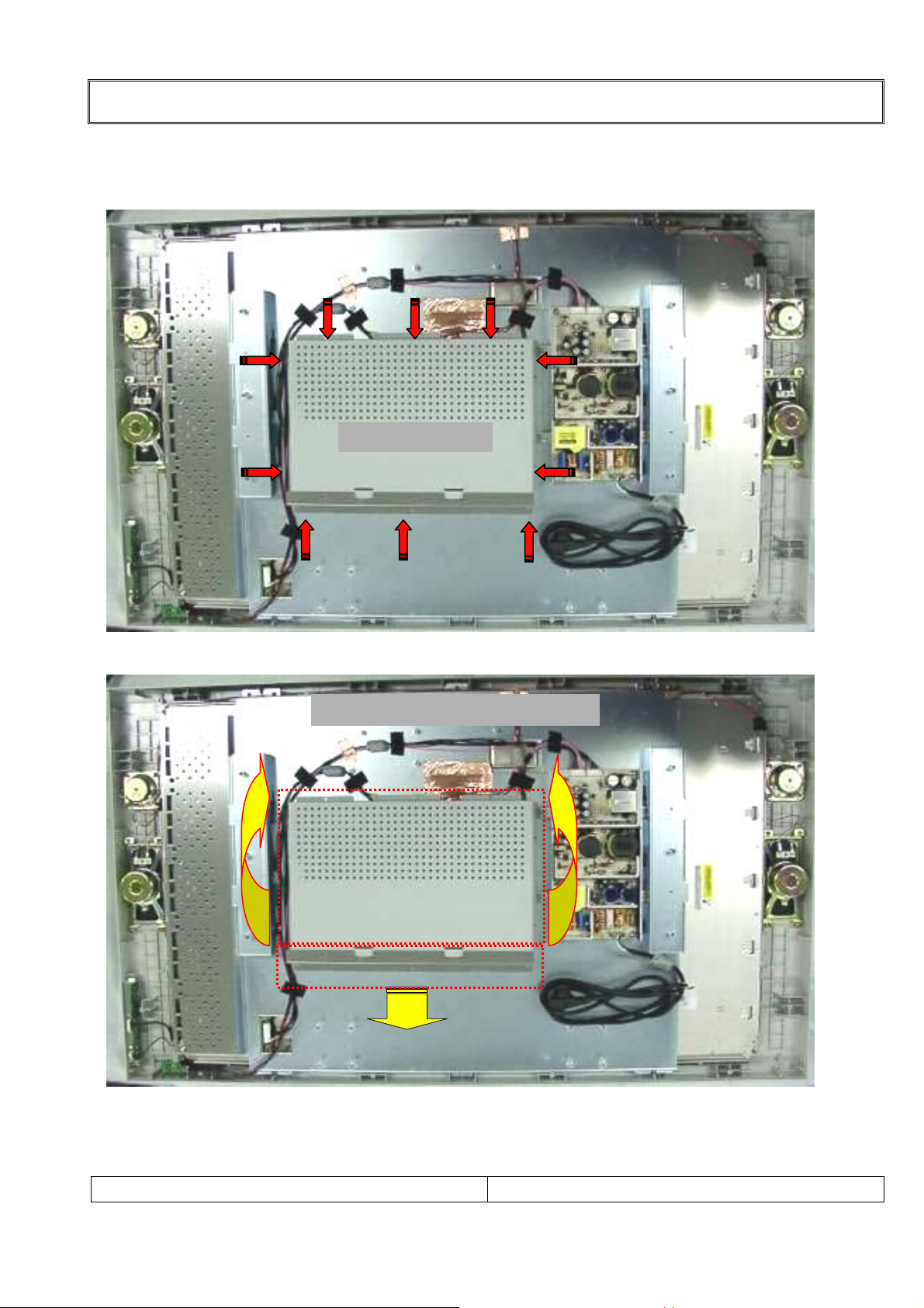
DISASSEMBLY PROCEDURE
2-1). Metal plate & Rear chassis
Remove 10 Screw
Removal of Rear & Terminal metal plate
SERVICE MANUAL
PAGE:
13
Page 14
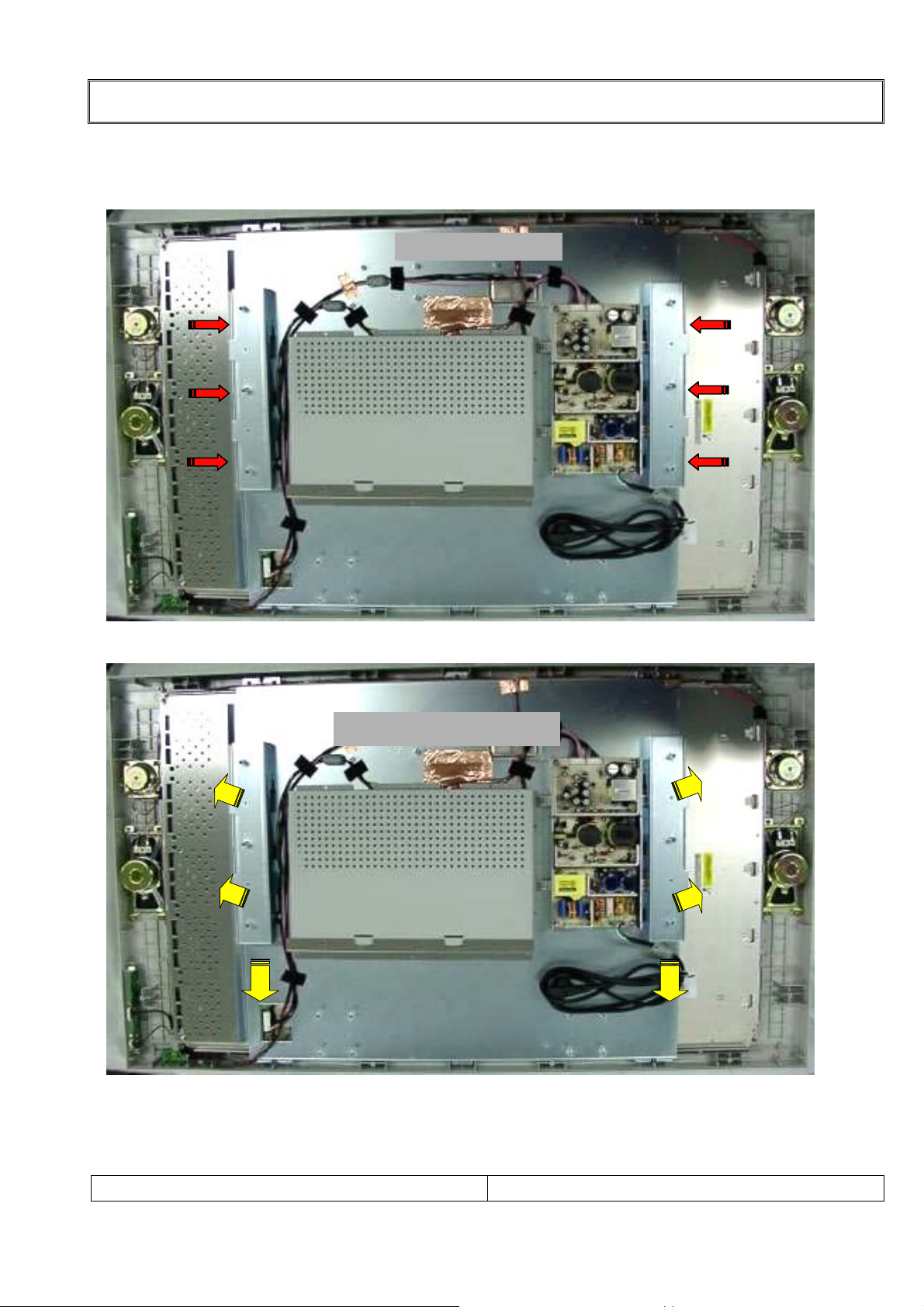
DISASSEMBLY PROCEDURE
2-2). Metal plate & Rear chassis
Remove 6 Connectors
Removal of Mount metal plate
SERVICE MANUAL
PAGE:
14
Page 15
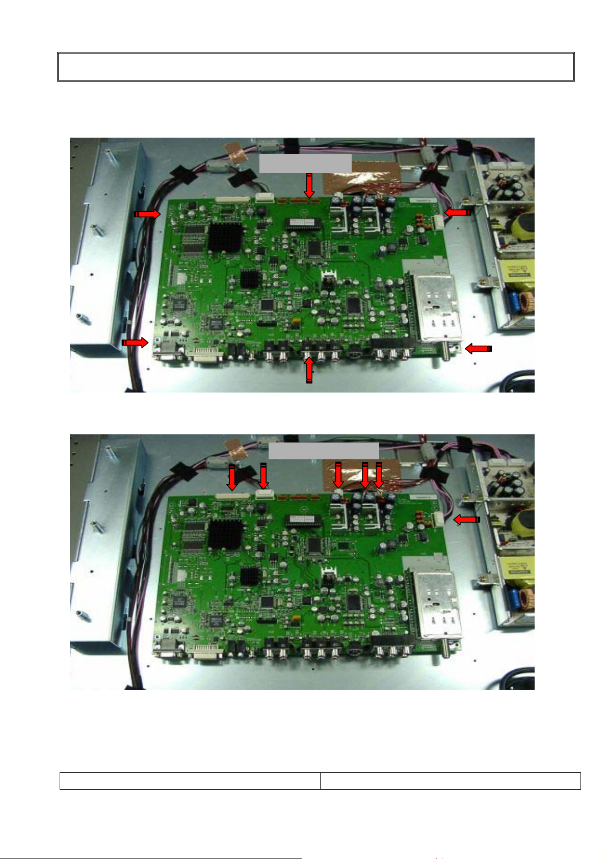
DISASSEMBLY PROCEDURE
3).Main PWB & Connectors
Remove 6 Screw
Remove 6 Connectors
SERVICE MANUAL
PAGE:
15
Page 16
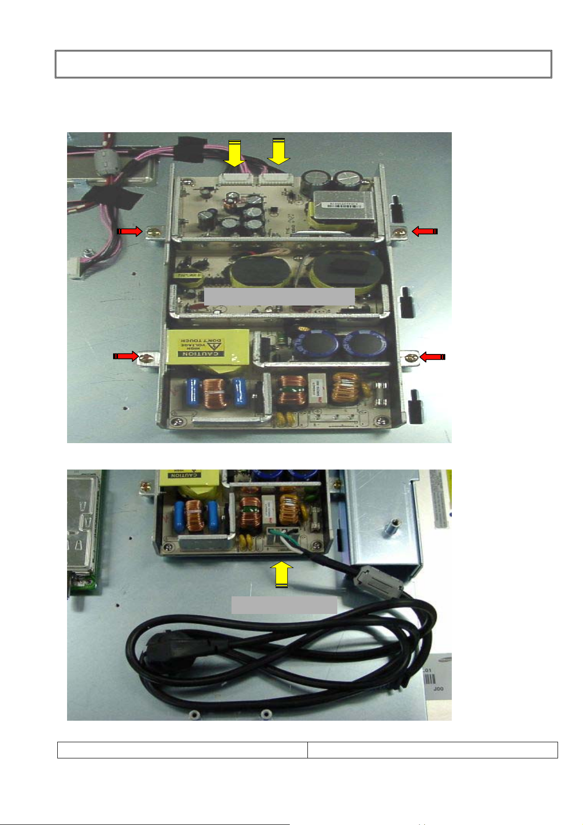
DISASSEMBLY PROCEDURE
4). SMPS Board & Power cord
Remove 4 Screw & 2 Connectors
Remove Power Cord
SERVICE MANUAL
PAGE:
16
Page 17
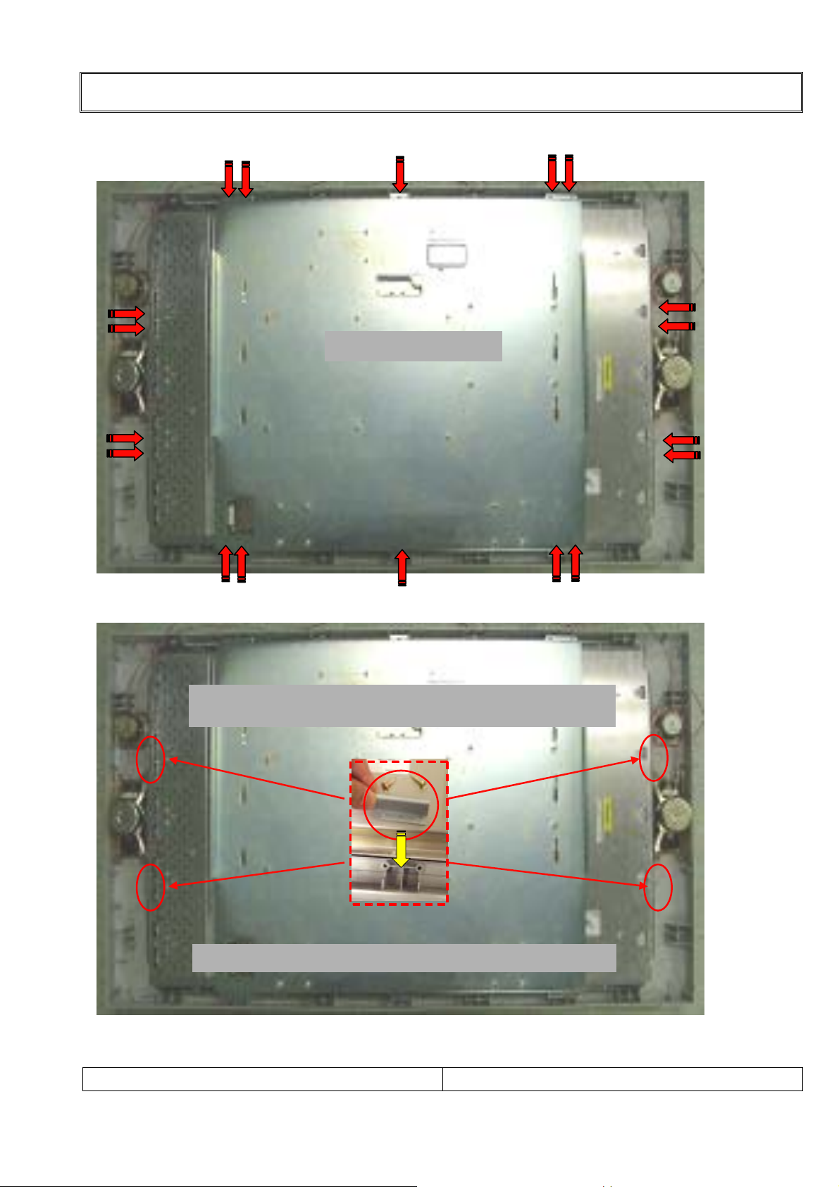
5-1). LCD Module
DISASSEMBLY PROCEDURE
Remove 14 Screw
Remove 4 brackets, then lift out LCD Module
Removal of LCD Panel module mounting brackets
SERVICE MANUAL
PAGE:
17
Page 18
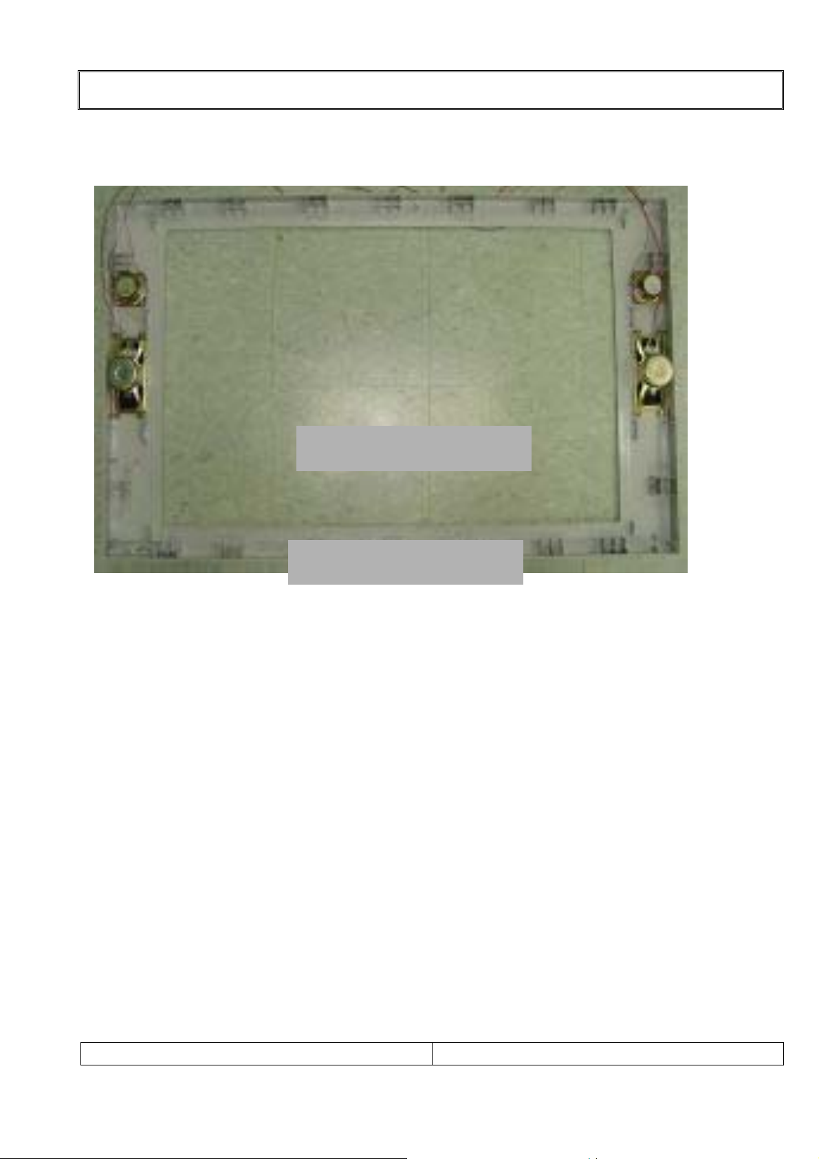
5-2). LCD Module
DISASSEMBLY PROCEDURE
Front mask remains after
removing LCD Module
Front mask remains after
removing LCD Module
SERVICE MANUAL
PAGE:
18
Page 19
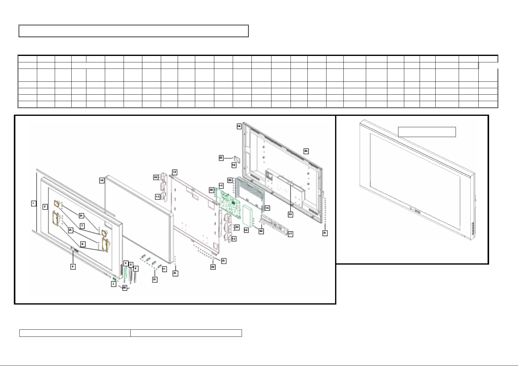
MECHANICAL EXPLODED VIEW
1. Explode View
N0 1 2 3 4 5 6 7 8 9 10 11 12 13 14 15 16 17 18 19 20 21 22 23 24 25
PART
NAME
DESCRIPTIO
DECO(T,B)
N
MATERIAR PMMA PC+ABS - - ABS PVC - - NI SAMSUNG EGI EGI EGI - - EGI SPTH PC+ABS ABS PVC SZN SZN SZN SZN SZN
COLOR
FISH
Q'TY (EA) EACH 1 1 1 1 1 1 2 2 1 1 4 1 EACH 1 1 1 1 1 1 1 1 50 7 3 14 21
REMARK CONTROL REAR
402-
400-011T AYCOLT32A01A 404-004A 450-001D 610-005A 610-005B 501-016T
004X,Y
FRONT CONTROL BLOCK DECO SPEAKER
IR PCB
COVER
MIRROR SILVER - - SILVER SILVER - - SILVER - - - - - - - - DARK GRAY DARK GRAY BLACK - - - - -
PCB KNOB PLATE 20W, 8Ω 10W, 8Ω LOGO
SPEAKE
R STICKER SHIELD SHIELD MAIN PCB AC/D C SHIELD SHIELD BACK CORD DECO SCREW SCREW SCREW SCREW SCREW
PANV400W100
407-004F 407-004G 407-004L
0
PANEL FIX BRKT
AYMALT34A01
FRONT MOUNT(L,R) ASS'Y ADAPTER REAR JACK COVER HOLDER PLATE BTB 4*12 TTB 3*8 PBTB 3* 10 PB 4*8 PB 3*6
620-005A 407-004H 407-004J 401-00 3A 402-004Z 450-002C-
A
410-
410-001K 410-002L 410-001R 410-002C
001Q
TAPPING TAPPIN
TAPPING MACHINE MACHINE
G
SET ASS'Y
SERVICE MANUAL
PAG E:
19
Page 20
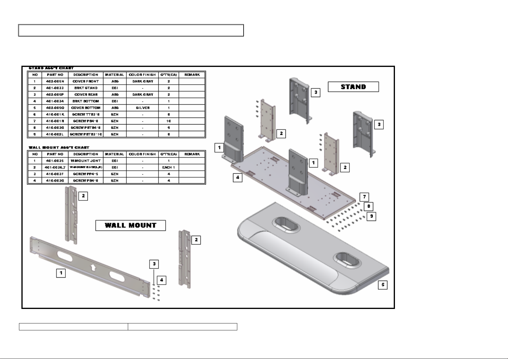
1-1,. Explode View
- option
MECHANICAL EXPLODED VIEW
SERVICE MANUAL
PAG E:
20
Page 21
CIRCUIT DESCRIPTIONS
General Description for 40.0” color TFT LCD TV.
The TFT LCD TV described in the followings is based on a Multi TV system, digital
Control display, 40.0” diagonal. The TFT LCD TV is intended to be a finished product,
Basically a display device mounted inside an enclosure which will provide the safety
Requirements. With the exception of LCD Panel, the display device shall be composed
entirely of solid state components.
These components shall have a history of reliable service in identity applications
and shall be applied in the circuits.
1. SCALER SECTION.
2. MCU SECTION.
3. ADC SECTION.
4. VIDEO PROCESSOR SECTION.
5. FRAME RATE CONVETER SECTION.
6. AUDIO PROCESSOR SECTION.
NOTE: ROM is two types, To development early stage it used the EEPROM – AT29C020
The production used the OTP (EPROM – M27X201)
It follows in the ROM and the point which is changed
Apply ROM
AT29C020 (flash) IC01 L17 L15 600ohm BEAD
M27X201 (OTP) IC01 L15 L17 600ohm DEAD
SERVICE MANUAL
LOCATION NO
PART Insert PART Remove Description
21
PAGE:
Page 22
CIRCUIT DESCRIPTIONS
1.SCALER SECTION.
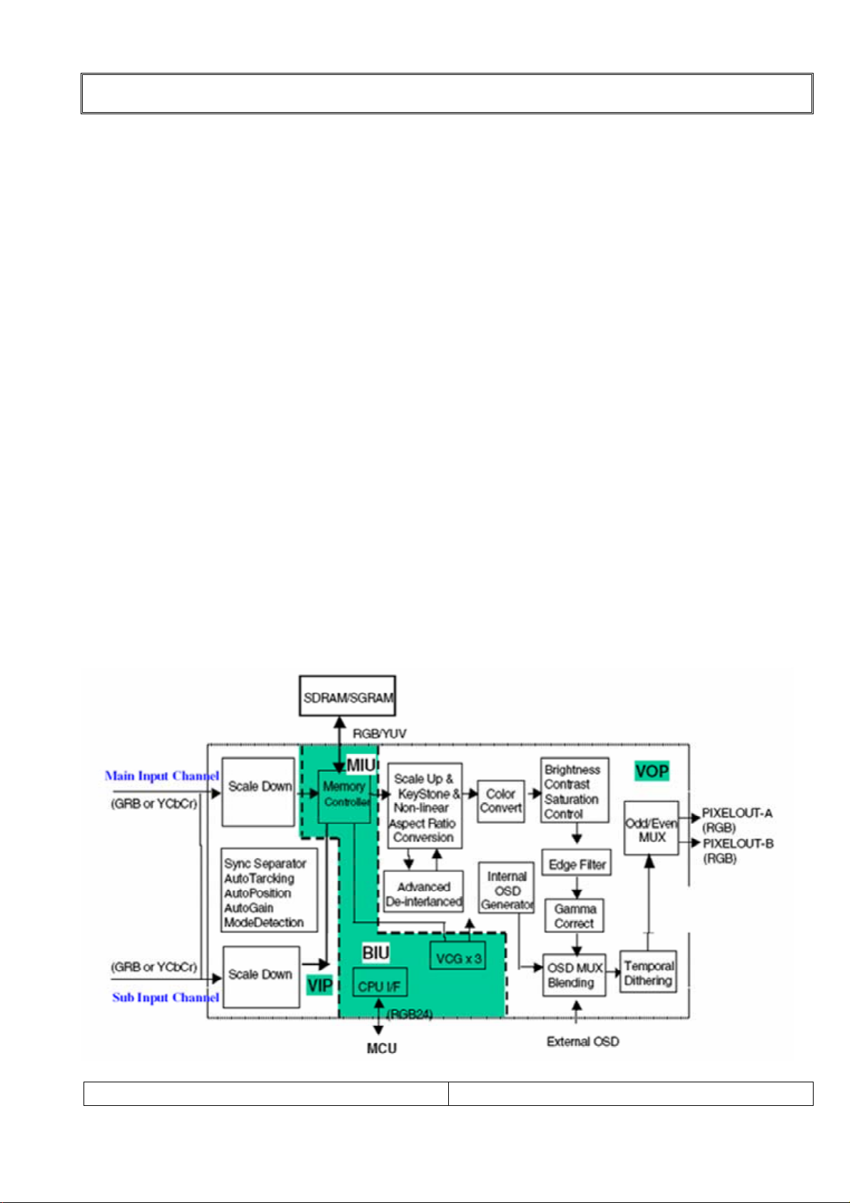
Device: MX88L285
Features: Advanced Image Scaling/ processing
Automatic Image Optimization
Frame buffer interface
Microprocessor interface
On-screen display
Color processing
8-bit display outputs
Main/Sub – input ports
1) Description
The highly flexible MX88L285 is the mixed-signal product from the display processors.
MX88L285 is a highly integrated display processor with advanced digital signal processing.
MX88L285 provides high design scalability by accepting input images from multiple
Sources and displaying them on any flat panel display.
For the conversion of VGA input signals to higher-resolution outputs, the MX88L285
uses a Smart-scaling TM -3 filter scaling algorithm that accepts programmable parameters
for horizontal and vertical scaling. The MX88L285 scaling engine allows text and graphics
images to be handled appropriately with different scaling algorithms.
Image centering is supported for applications where image manipulation is not needed.
The MX88L285 flexible SDRAM/SGRAM interface is designed to support VGA to
WXGA resolution panels to provide a cost-effective solution.
Fabricated in an advanced CMOS process, the MX88L285 is provided in a space-saving
–388-lead PBGA surface-mount plastic package.
2) Block Diagram.
SERVICE MANUAL
PAGE:
22
Page 23
CIRCUIT DESCRIPTIONS
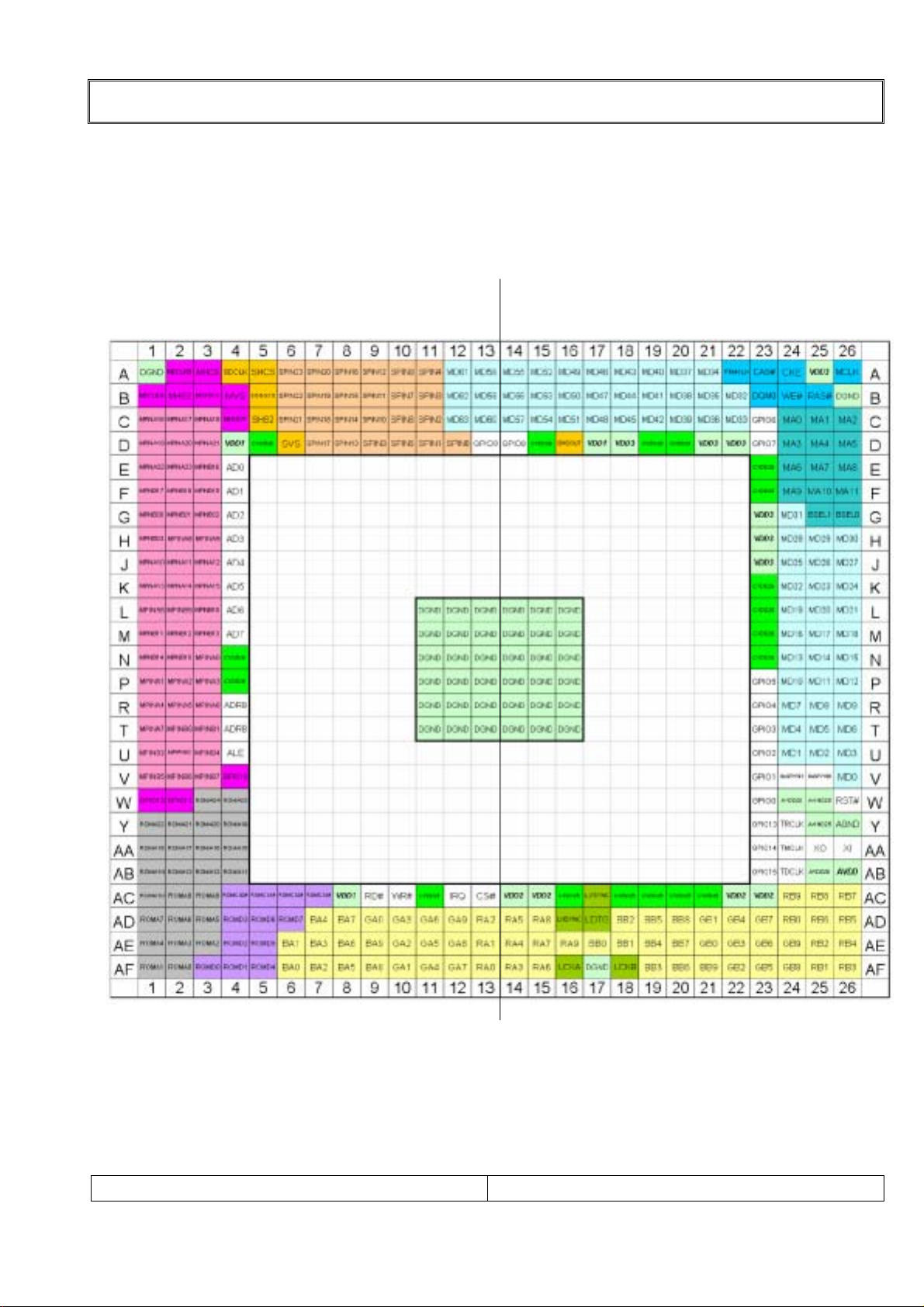
3)Pin configuration.
Reference line
The left side The right side
SERVICE MANUAL
PAGE:
23
Page 24
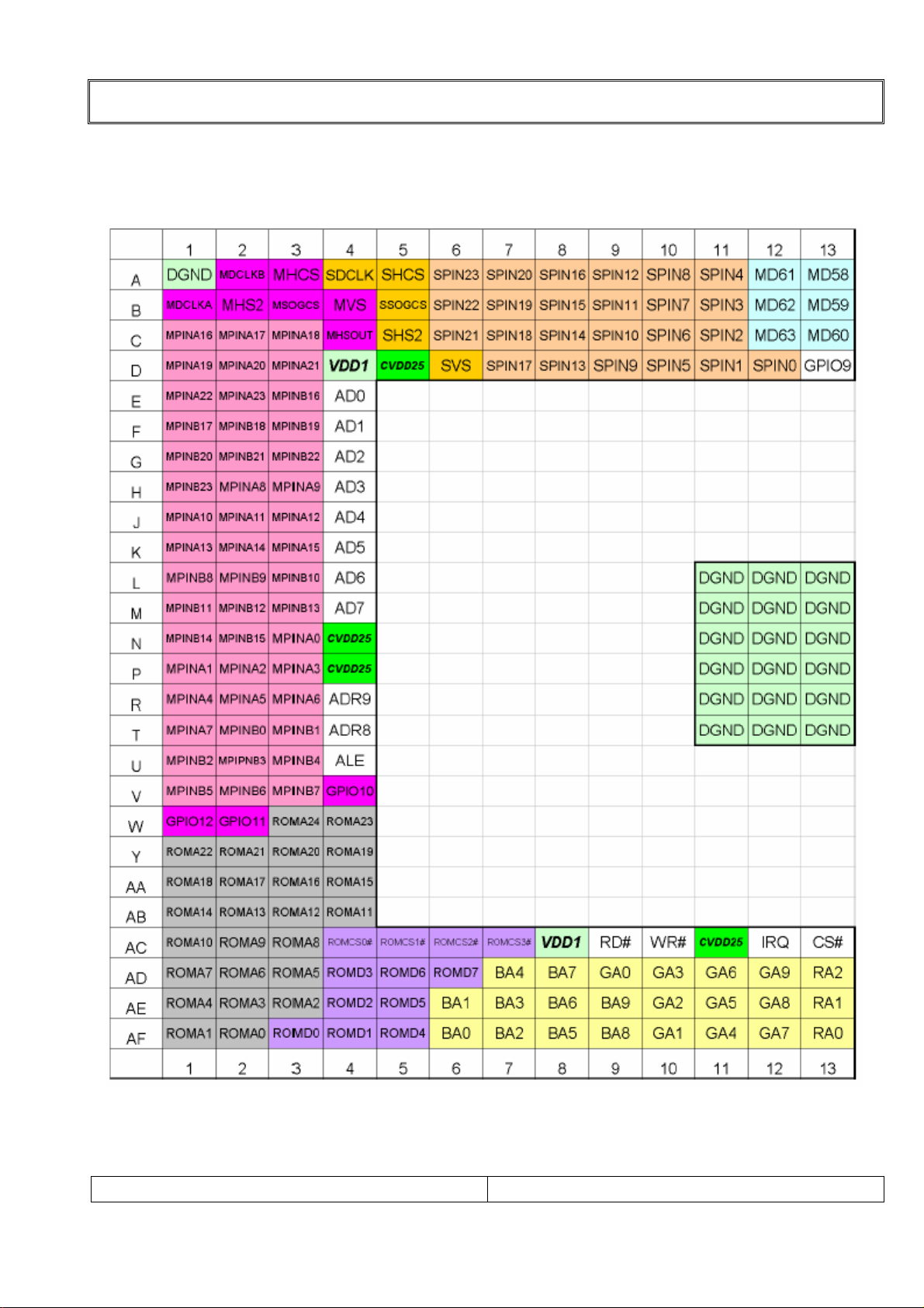
3-1) Pin configuration
< The left side >
CIRCUIT DESCRIPTIONS
SERVICE MANUAL
PAGE:
24
Page 25
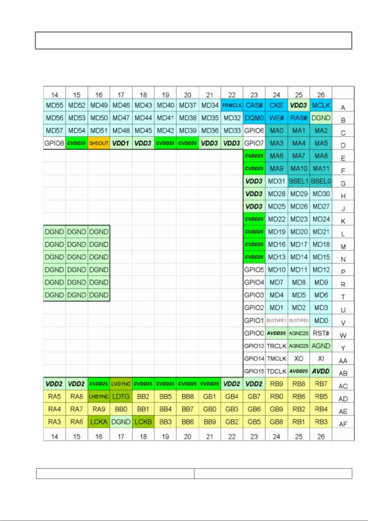
3-2) Pin configuration
< The right side >
CIRCUIT DESCRIPTIONS
SERVICE MANUAL
PAGE:
25
Page 26
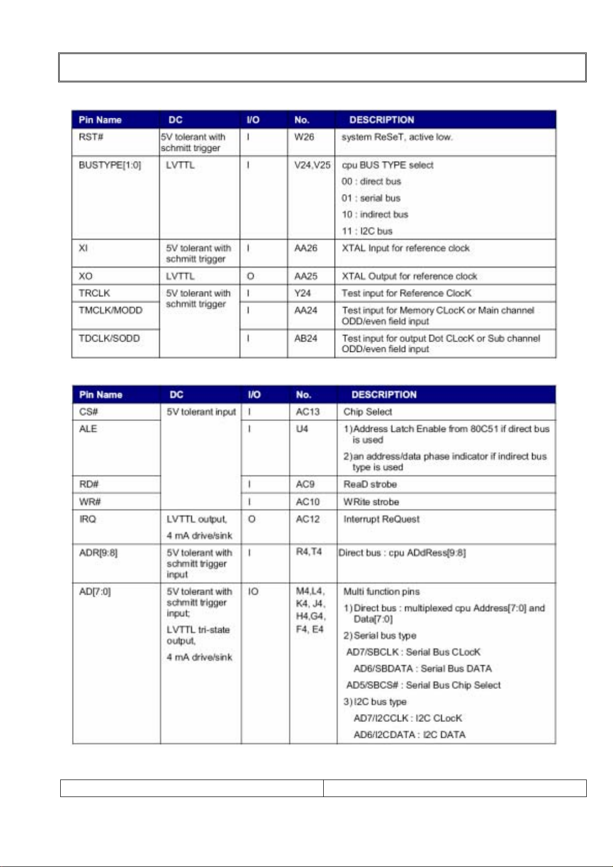
4)Pin Functions.
[ General Interface Pins ]
CIRCUIT DESCRIPTIONS
[ MCU (CPU ) interface Pins . ]
SERVICE MANUAL
PAGE:
26
Page 27
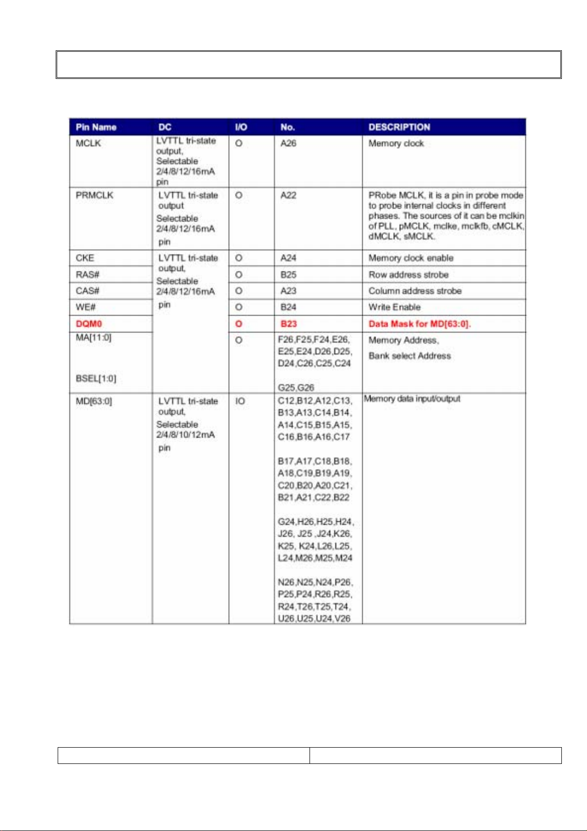
[ SDRAM / SGRAN interface Pins . ]
CIRCUIT DESCRIPTIONS
SERVICE MANUAL
PAGE:
27
Page 28
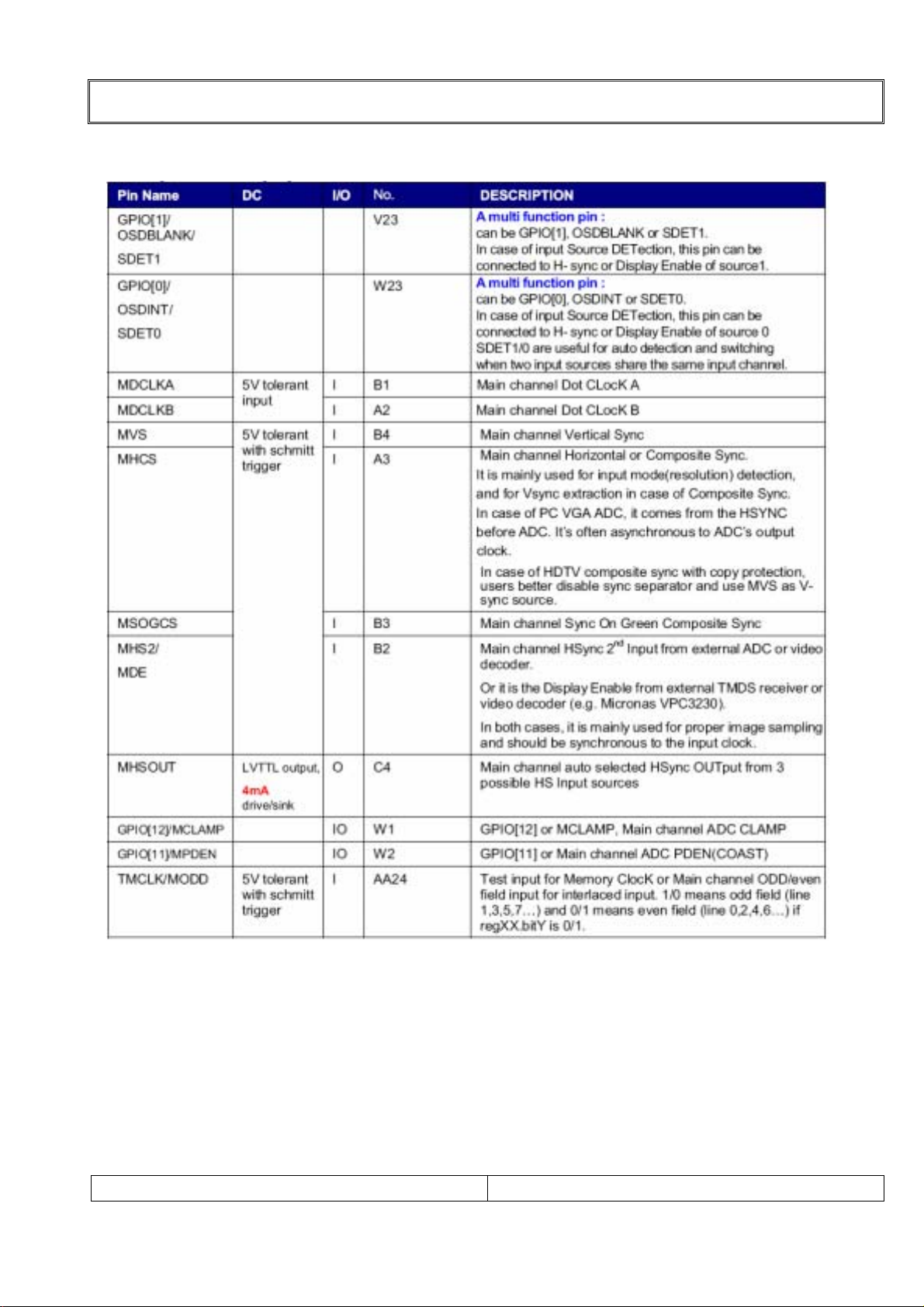
CIRCUIT DESCRIPTIONS
[1. Main Input Interface – input pins for Main stream ]
SERVICE MANUAL
PAGE:
28
Page 29
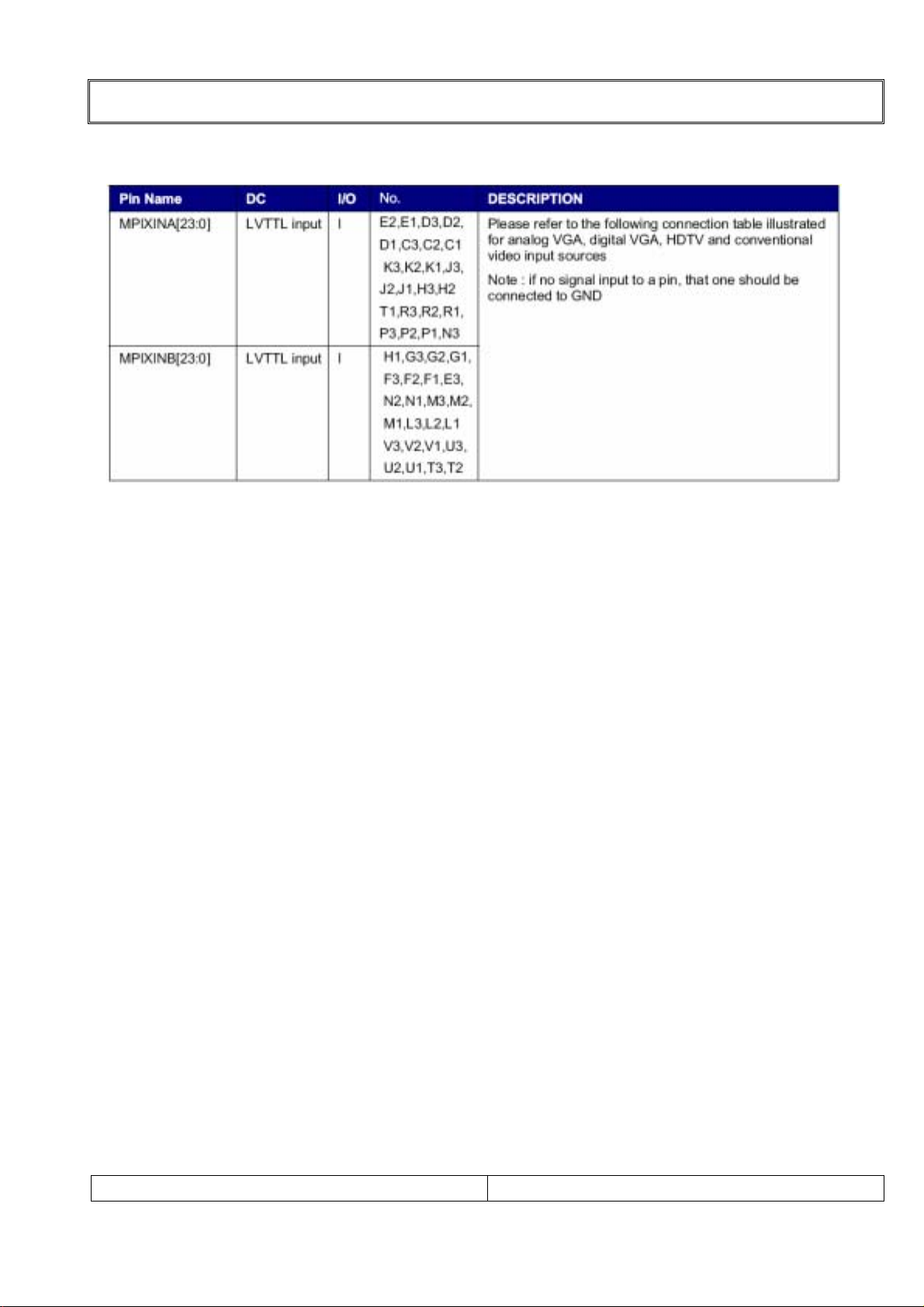
CIRCUIT DESCRIPTIONS
[2. Main Input Interface – input pins for Main stream ]
SERVICE MANUAL
PAGE:
29
Page 30
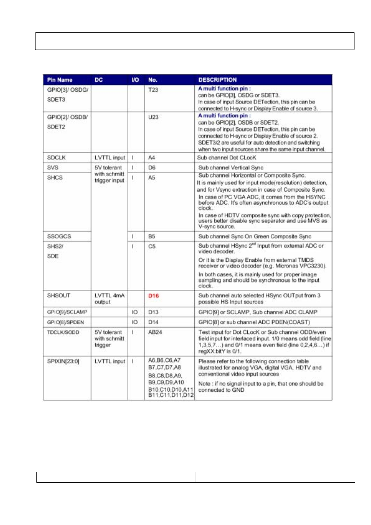
CIRCUIT DESCRIPTIONS
[ Sub Input Interface – input pins for Sub stream ]
SERVICE MANUAL
PAGE:
30
Page 31
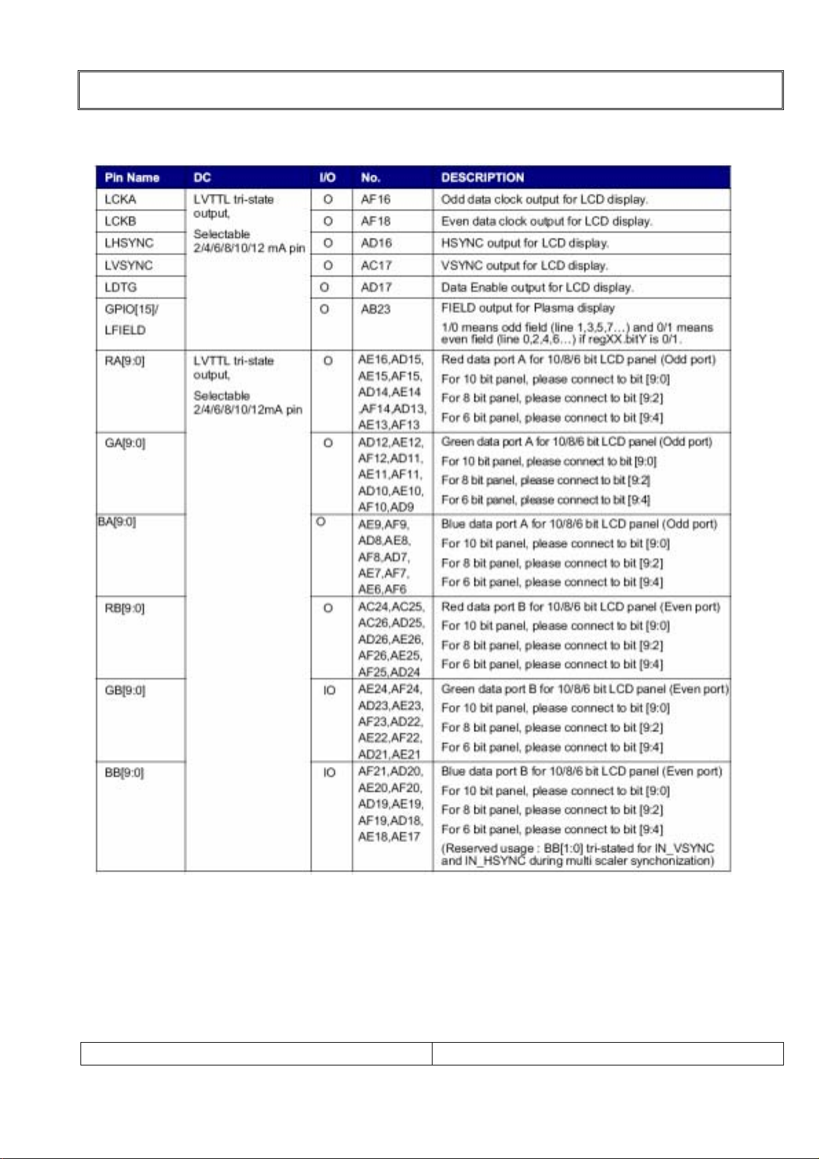
[Display output interface]
CIRCUIT DESCRIPTIONS
SERVICE MANUAL
PAGE:
31
Page 32
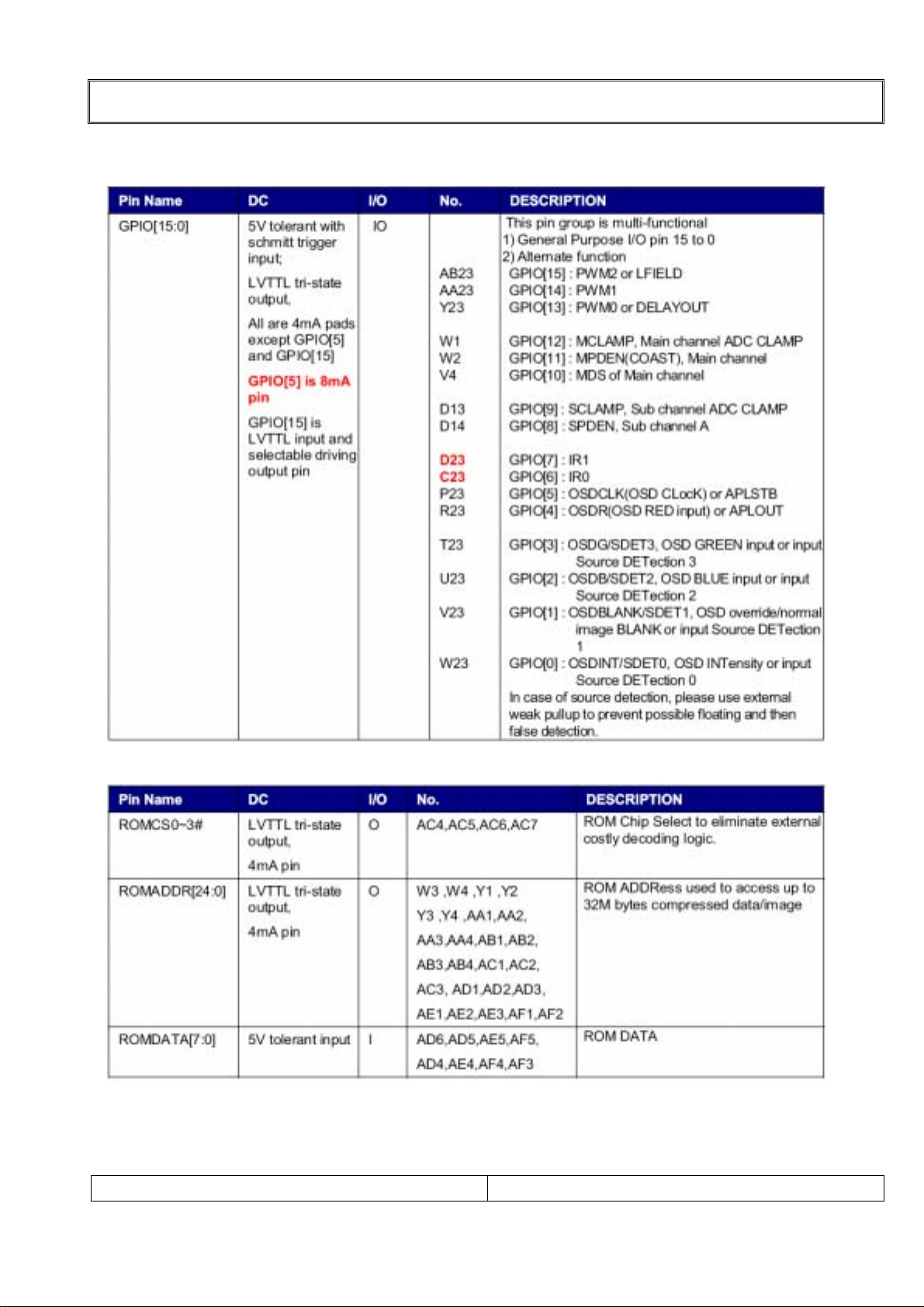
CIRCUIT DESCRIPTIONS
[Muti- function and General Input/Output Interface]
[Auto-load Power – on screen Interface]
SERVICE MANUAL
PAGE:
32
Page 33
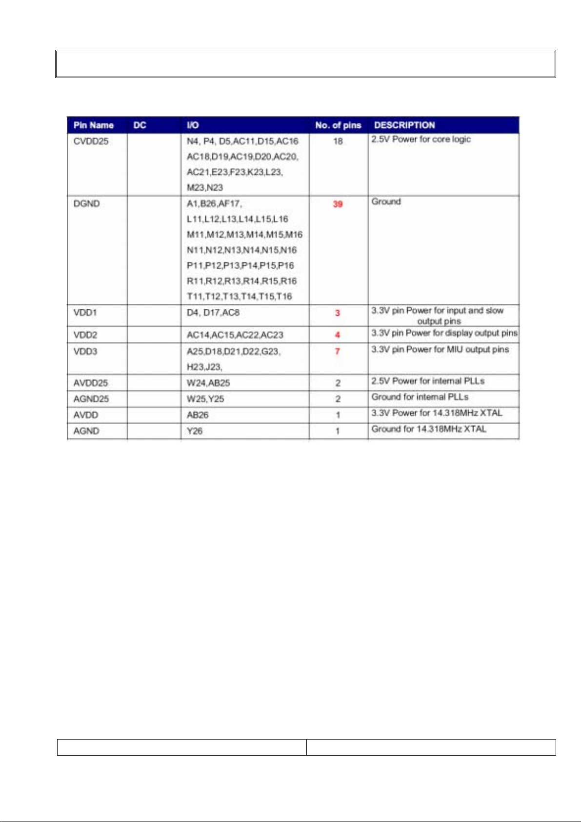
[Power – ground pins]
CIRCUIT DESCRIPTIONS
SERVICE MANUAL
PAGE:
33
Page 34
CIRCUIT DESCRIPTIONS
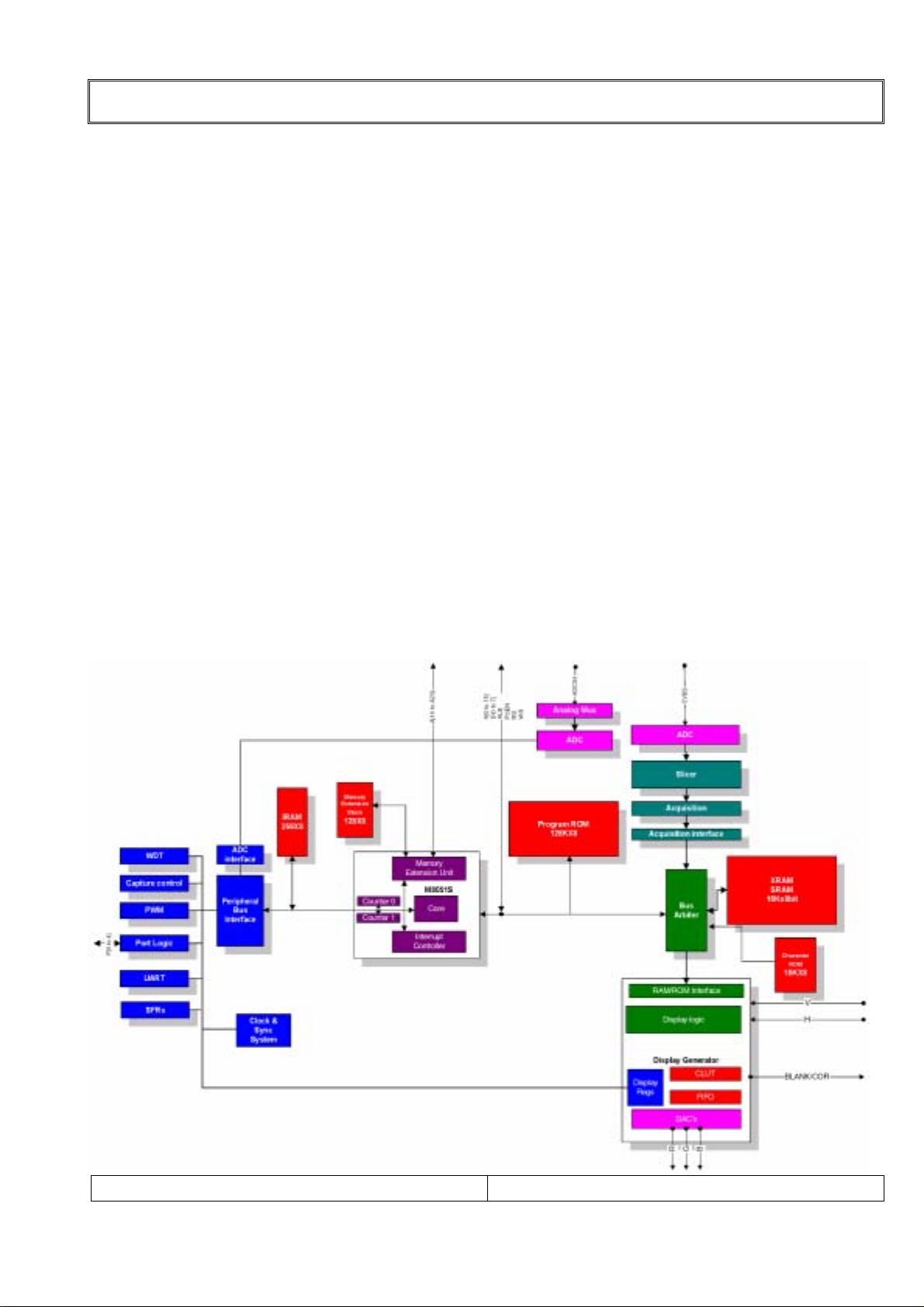
2. MCU SECTION.
Device: SDA55XX
Features: Built-in teletext decoder.
8051 compatible.
Internal ROM type.
1) Description
The device provides an integrated general-purpose,fully 8051-compatible Microcontroller
with televisionspecific hardware features. Microcontroller has beenenhanced to provide
powerful features such as memory banking, data pointers and additional interruptsetc.
Internal XRAM consists of up to 16 Kbytes. Devicehas an internal ROM of up to 128
Kbytes.
The SDA 55xx supports a wide range of standardsincluding PAL, NTSC and contains a
digital slicer forTeletext and Closed Caption.
Fabricated in an advanced CMOS process, the SDA55XX is provided in PMQFP64 SMD
type plastic package.
2) Block Diagram.
SERVICE MANUAL
PAGE:
34
Page 35
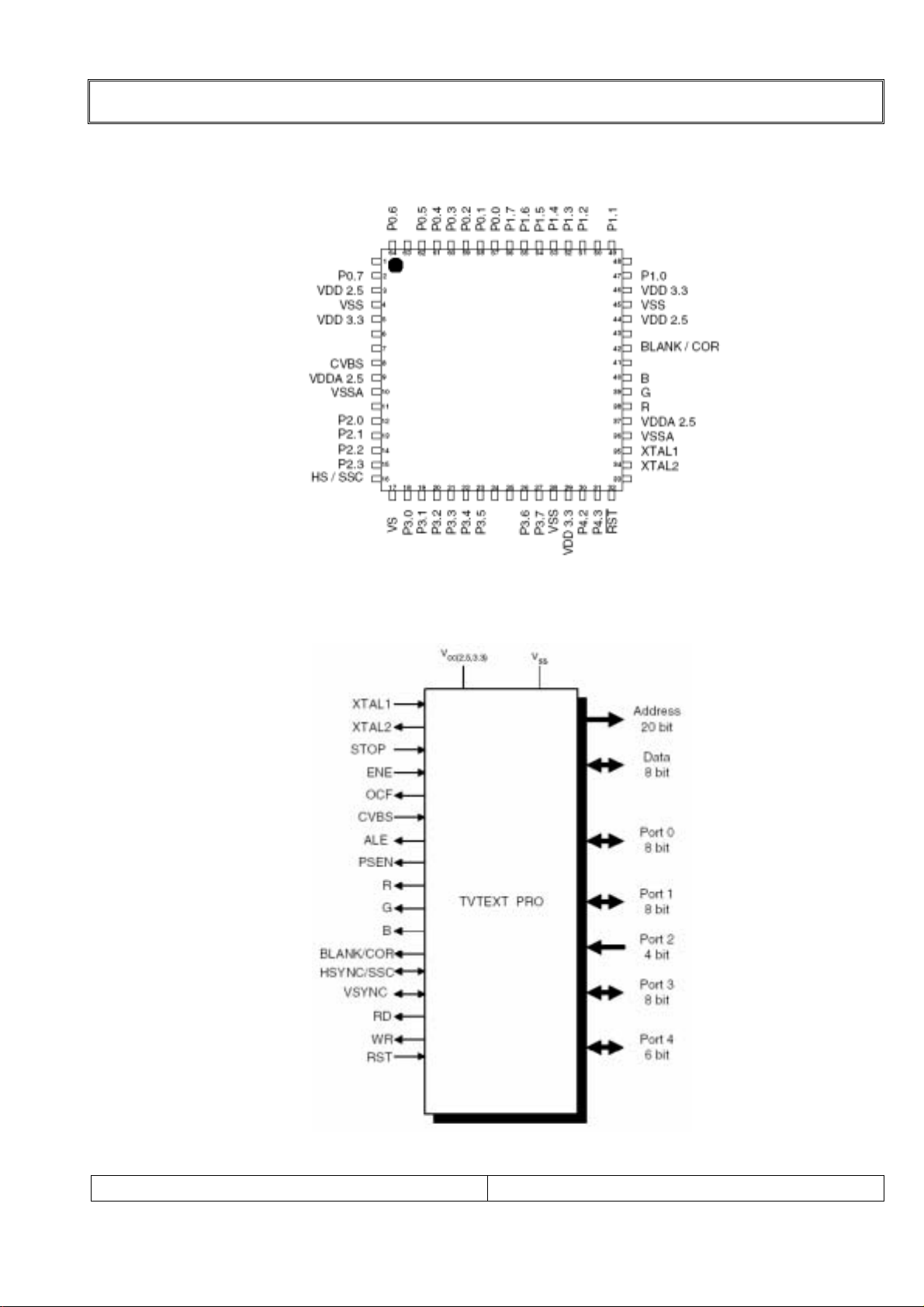
3)Pin configuration.
CIRCUIT DESCRIPTIONS
[ Pin configuration PMQFP64]
[ Logic symbol ]
SERVICE MANUAL
PAGE:
35
Page 36
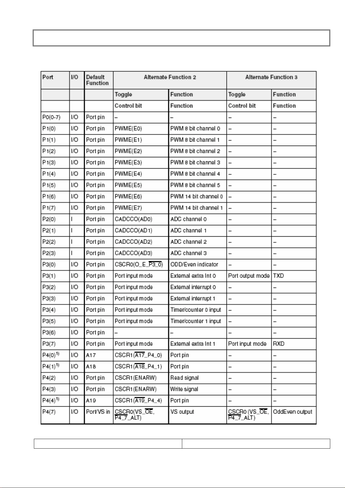
4) Pin(Port) Functions
CIRCUIT DESCRIPTIONS
SERVICE MANUAL
PAGE:
36
Page 37

CIRCUIT DESCRIPTIONS
3. ADC SECTION.
Device: AD9882KST – 100.
Features: RGB Graphics Processing (A/D Converter).
Scan Converters.
Horizontal & Vertical Sync Processing
Digital Visual Interface
1) Description
Analog Interface
The AD9882 is a complete 8-bit, 100 MSPS monolithic analog interface optimized for
capturing RGB graphics signals from personal computers, workstations and DTV STB. Its
100MSPS encode rate capability and full power analog bandwidth of 300 MHz
supports resolutions up to WXGA (1280 × 768).
The AD9882 includes a 100 MHz triple ADC with internal1.25 V reference, a PLL, and
programmable gain, offset, and clamp control.
The AD9882 also offers full sync processing for composite sync and sync-on-green
applications. A clamp signal is generated internally or may be provided by the user
through the CLAMP input pin. This interface is fully programmable via a 2-wire serial
interface (I2C).
Fabricated in an advanced CMOS process, the AD9882 is provided in a space-saving
100-lead LQFP surface-mount plastic package.
Digital Inter face
The AD9882 contains a DVI 1.0 compatible receiver and supports display resolutions
Up to SXGA (1280 x 1024 ). The receiver features an intra-pair skew tolerance of up to
One full clock cycle
With the inclusion of HDCP, displays may now receive encrypted video content.
The AD9882 allows for authentication of a video receiver, decryption of encoded data
At the receiver, and renew-ability of that a authentication during transmission as
specified by the HDCP v1.0 protocol
SERVICE MANUAL
PAGE:
37
Page 38
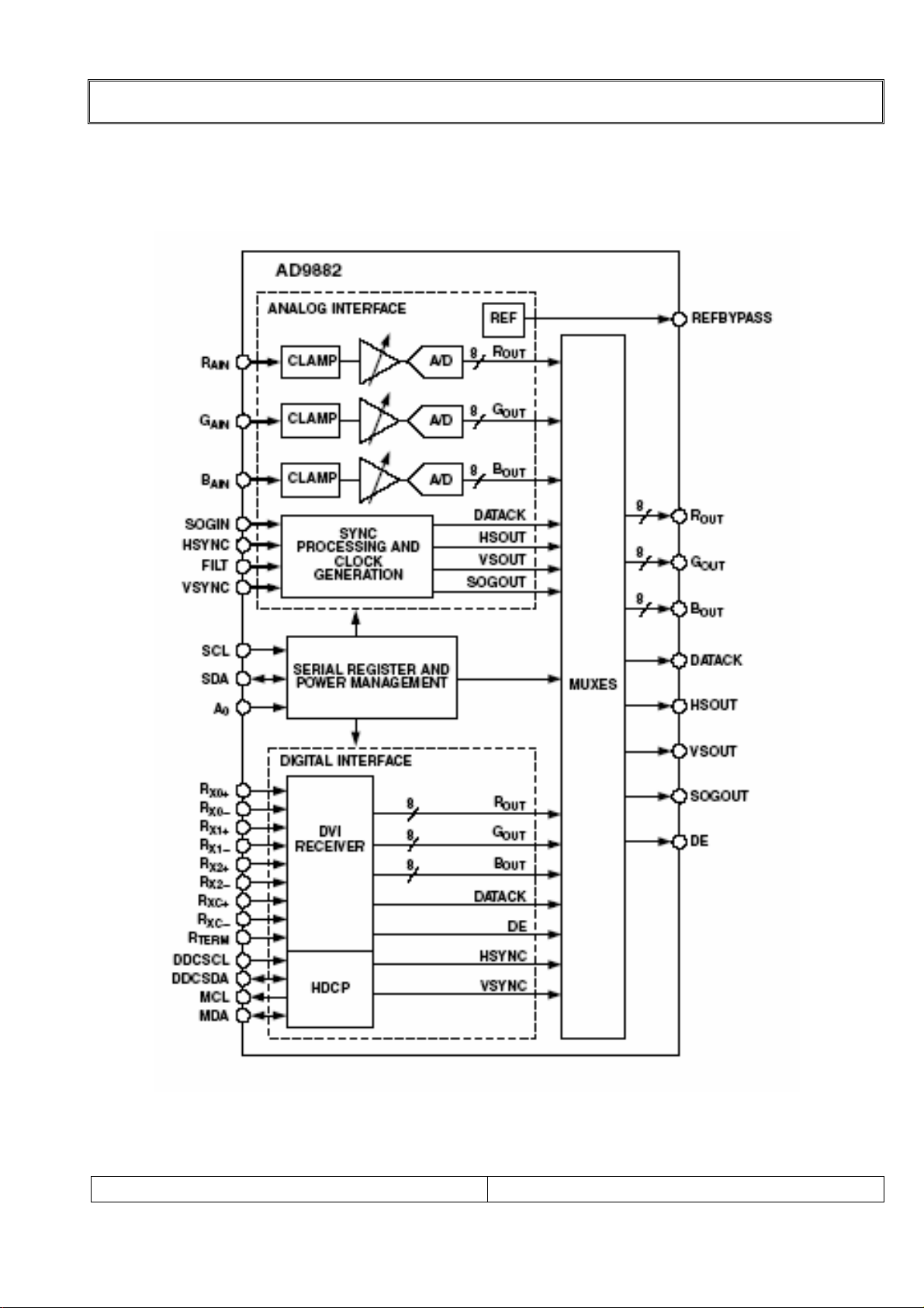
2) Block Diagram.
CIRCUIT DESCRIPTIONS
SERVICE MANUAL
PAGE:
38
Page 39
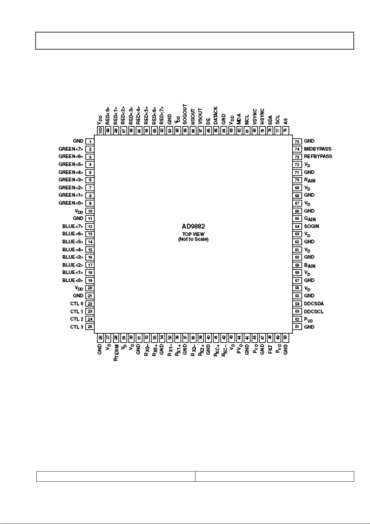
3) Pin configuration
CIRCUIT DESCRIPTIONS
SERVICE MANUAL
PAGE:
39
Page 40
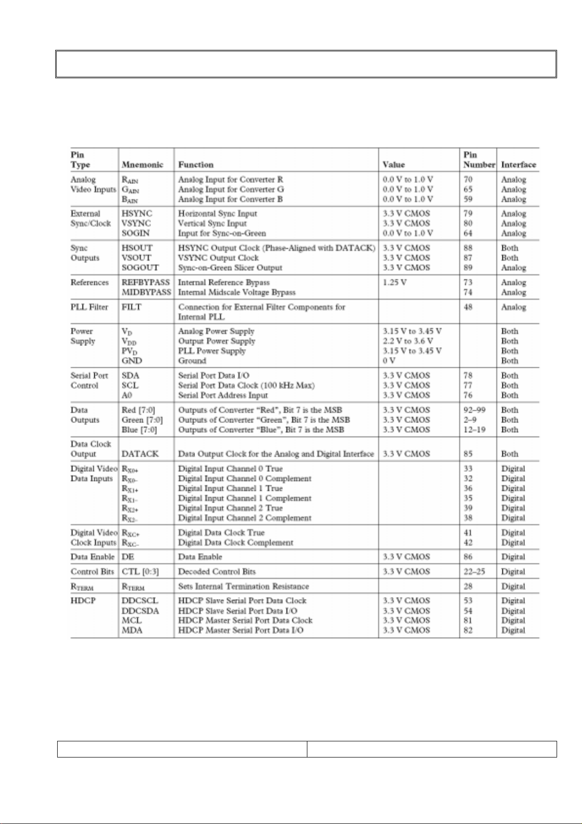
4) Pin Functions
CIRCUIT DESCRIPTIONS
SERVICE MANUAL
PAGE:
40
Page 41

CIRCUIT DESCRIPTIONS
4. VIDEO PROCESSOR SECTION.
Device: VSP 9417B
Features: Different application modes
Data acquisition connectivity
Multi-standard color decoder with 4H comb filter
Processing of two input channels independently
Second Multi-standard color decoder for slave channel
Scan-rate-conversion (version dependent)
Three D/A converters
Digital output
1) Description
50/60HZ derivatives are also avail-able. The device comprises digital multistandard color
decode for master and slave channel, a RGB interface with fast-blank capability (SCART),
scaling units including panorama, embedded DRAM for upcoversion high performance frame
based up conversion, High-performance frame based up conversion algorithms, picture
improvements, temporal noise reduction as well as A/D and D/A converter adaptive 4H comb
filter Y/C separator with adjustable vertical peaking
The either come form a CVBS, Y/C, RGB or YUV input or from a CCIR 656 compatible digital
input signal. For RGB and YUV, interlace and progressive signals up to XGA can be connected.
High resolution PC signals (SVGA, XGA etc.) may only be reproduced with limited picture
quality
Multi-standard color decoder PAL/NTSC/SECAM including all substandards.
Integrated high-quality A/D converters and associated clamp Multi-standard sync processing
Linear horizontal scaling as well as non-linear horizontal scaling
Peaking, contrast, brightness, color saturation and tint High-quality soft mixer controlled by Fast
Blank Control interface for external field memory I2C-Bus Interface
Fabricated in an advanced CMOS process, the VSP9417B is provided in a space-saving
QFP80 surface-mount plastic package.
SERVICE MANUAL
PAGE:
41
Page 42
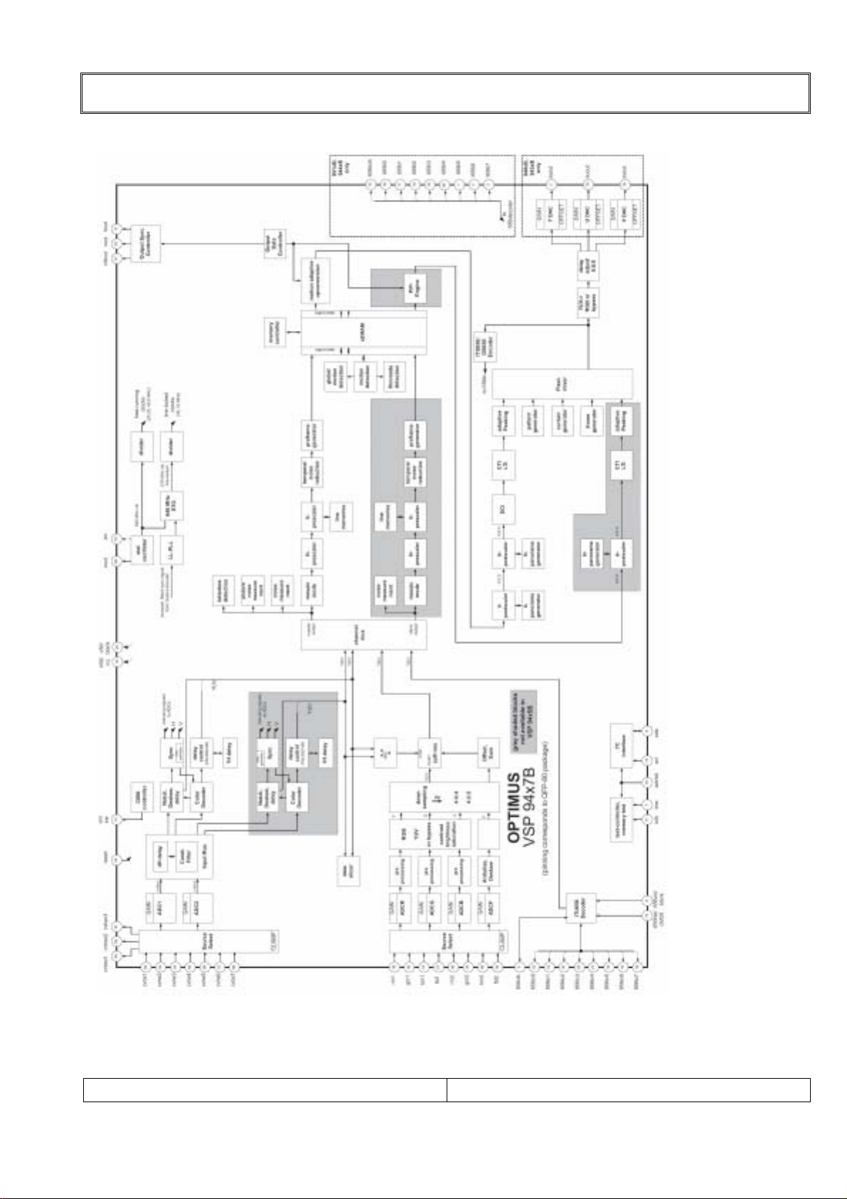
2) Block Diagram.
CIRCUIT DESCRIPTIONS
SERVICE MANUAL
PAGE:
42
Page 43
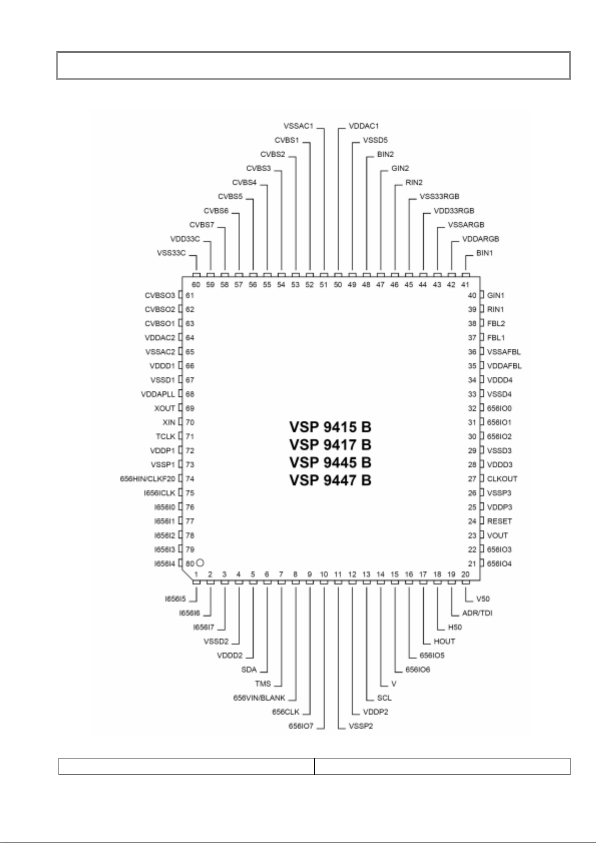
3)Pinconfigurations
CIRCUIT DESCRIPTIONS
SERVICE MANUAL
PAGE:
43
Page 44
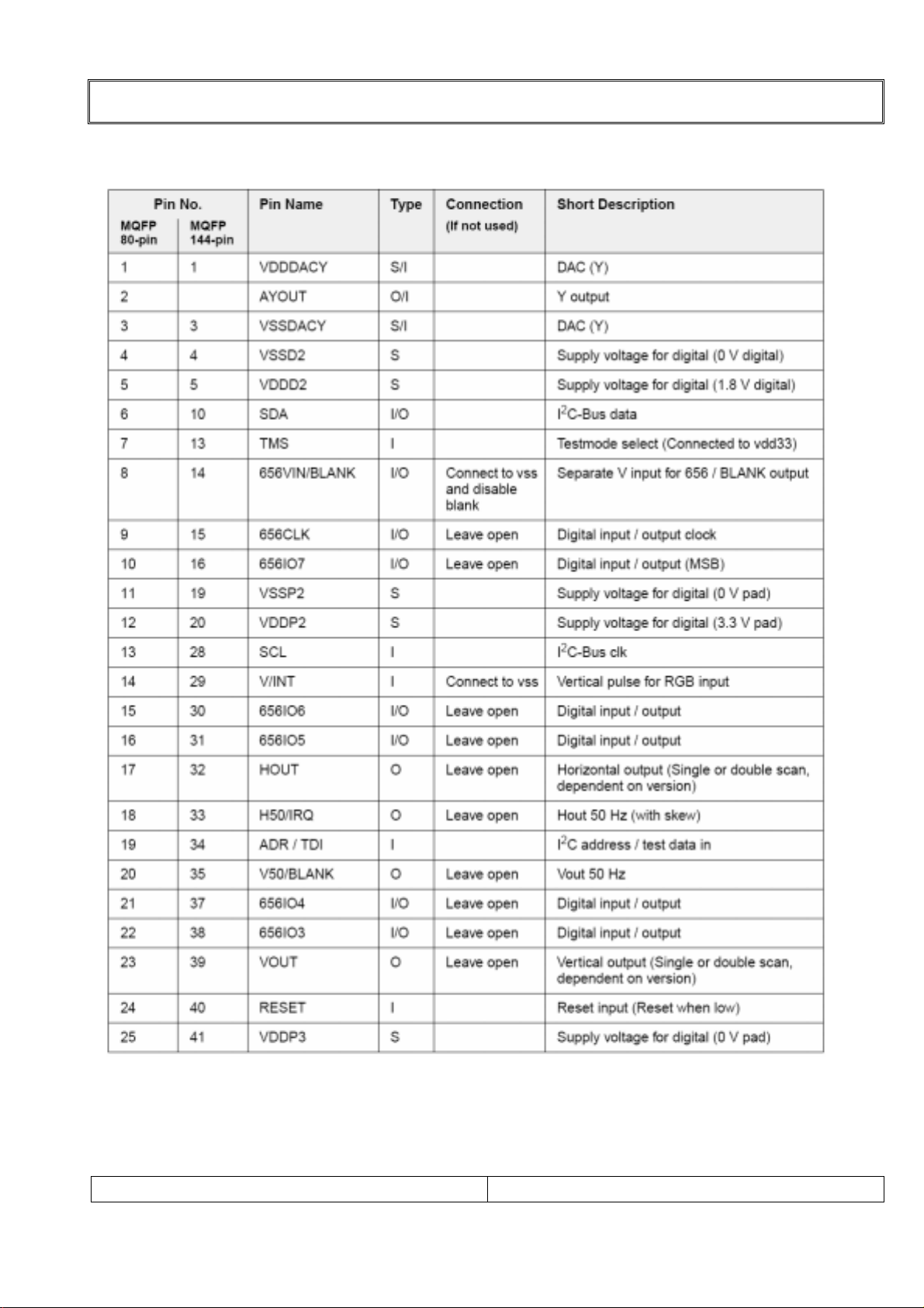
4-1) Pin Functions.
CIRCUIT DESCRIPTIONS
SERVICE MANUAL
PAGE:
44
Page 45
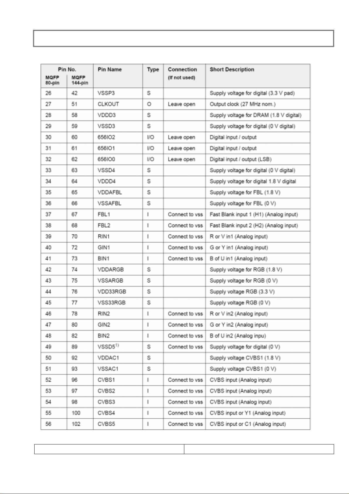
4-2) Pin Functions.
CIRCUIT DESCRIPTIONS
SERVICE MANUAL
PAGE:
45
Page 46
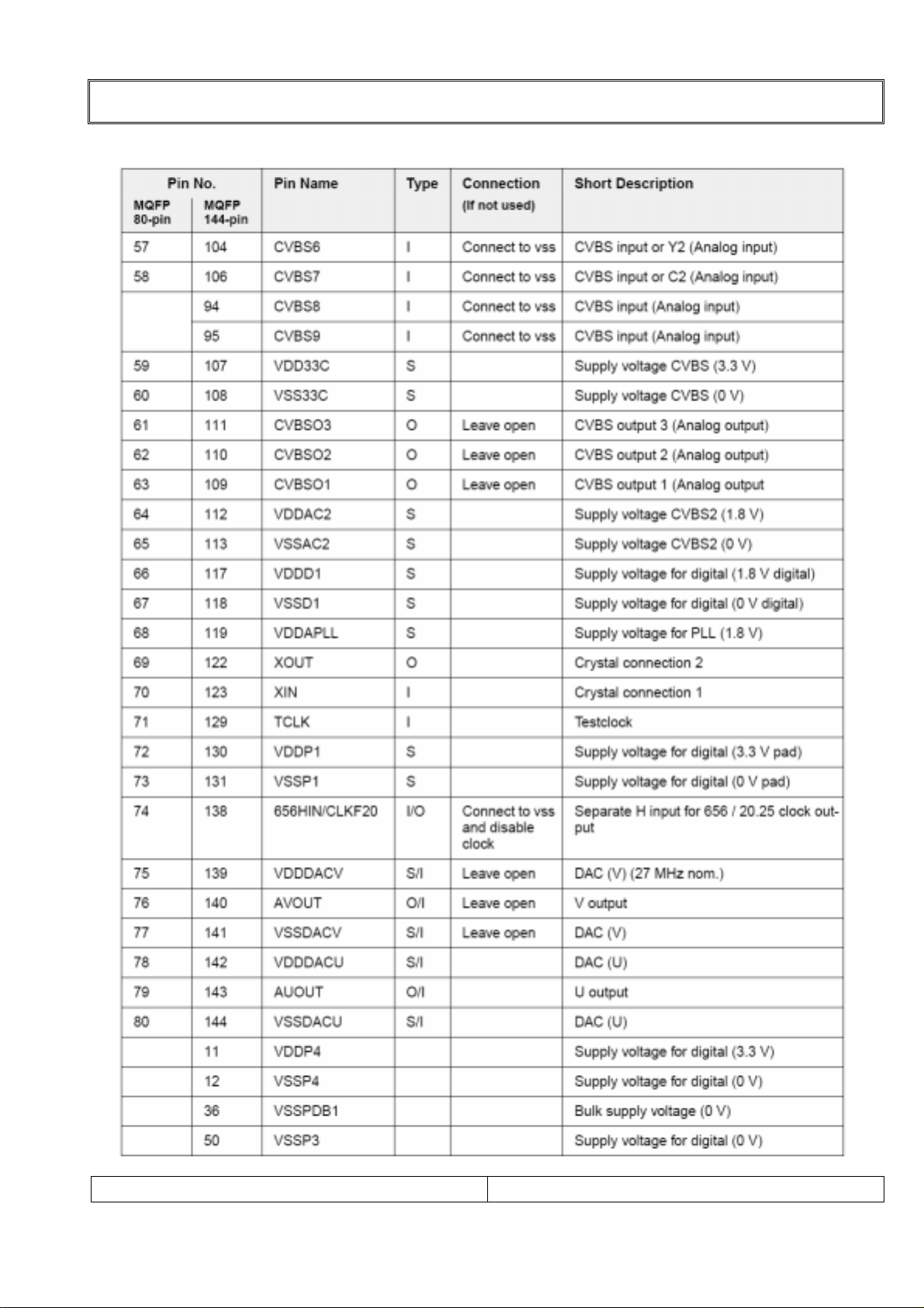
4-3) Pin Functions.
CIRCUIT DESCRIPTIONS
SERVICE MANUAL
PAGE:
46
Page 47
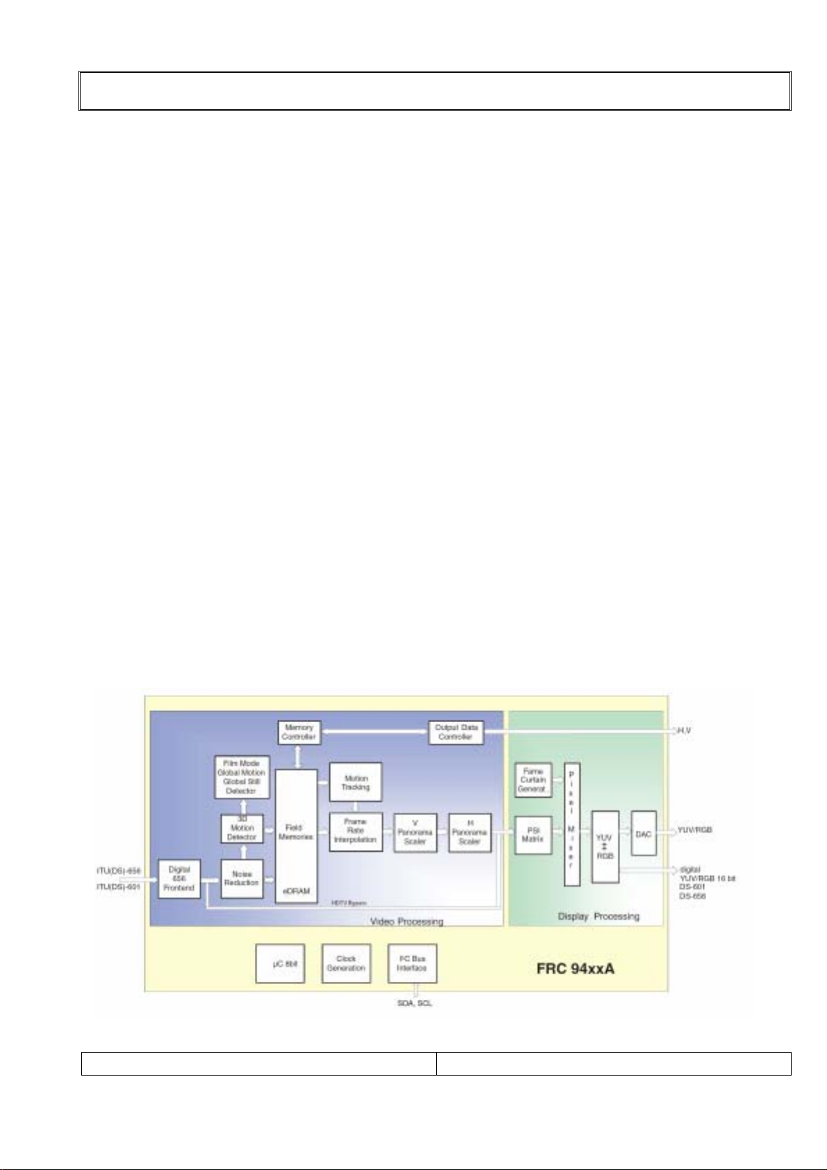
CIRCUIT DESCRIPTIONS
5. FRAME RATE CONVERTER SECTION.
Device: FRC 9429A
Features: Flim Judder Cancellation
Motion adaptive upconversion as global fall back
Automatic Film Mode Detection
Full internal 4:2:2 processing
656,601 compatible PAL/NTSC inputs and outputs
Embedded field memories
Macrovision encoding
Embedded 8-bit Microcontroller
1) Description
The FRC 94xxA comprises all mail functionalities of a high end frame rate converter in one
monolithic IC.
The FRC 94xxA is ideally suited to work in conjunction with different TV Deflection Processors
as DDP 3315/16C. Also operation with Deflection Processor from other sources is possible.
The device comprises digital input interfaces, embedded DRAM for frame rate conversion
algorithms, scaling units including panorama mode,picture improvement,temporal noise
reduction as well as digital and analog output interface
SERVICE MANUAL
PAGE:
47
Page 48
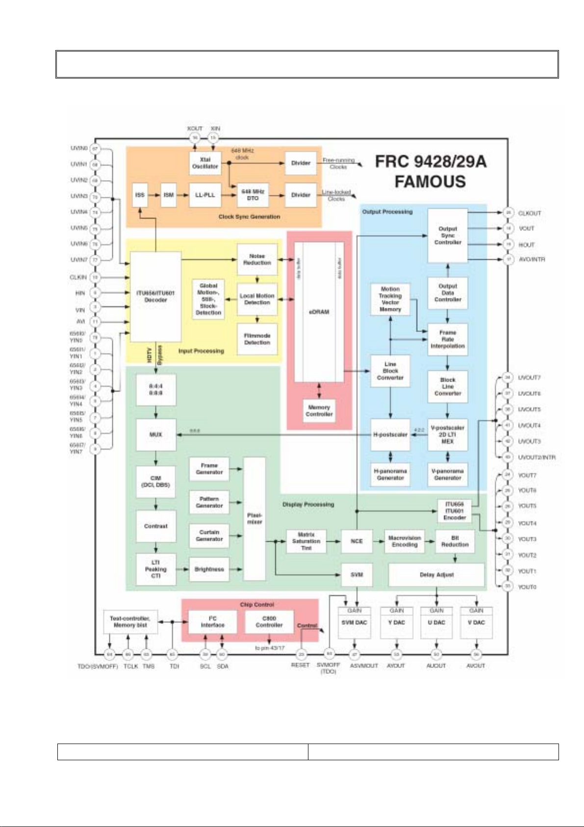
2) Block Diagram.
CIRCUIT DESCRIPTIONS
SERVICE MANUAL
PAGE:
48
Page 49
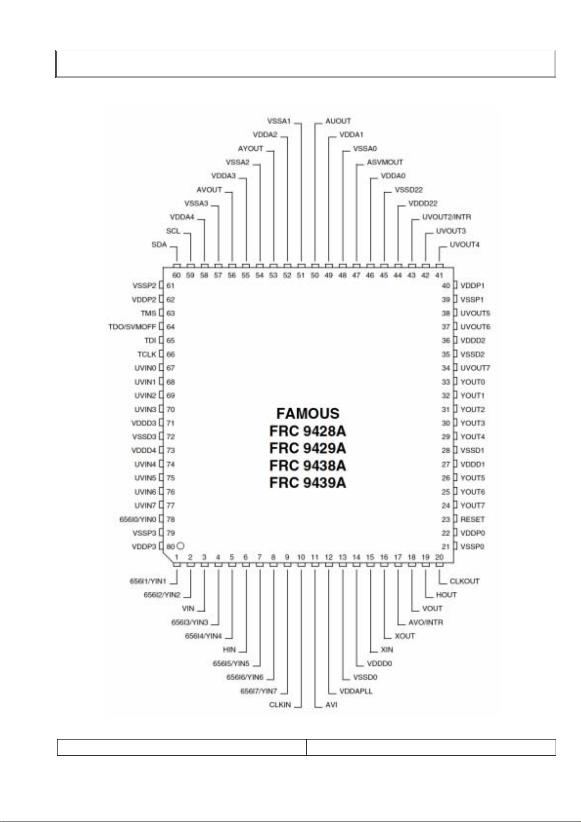
3)Pinconfigurations
CIRCUIT DESCRIPTIONS
SERVICE MANUAL
PAGE:
49
Page 50
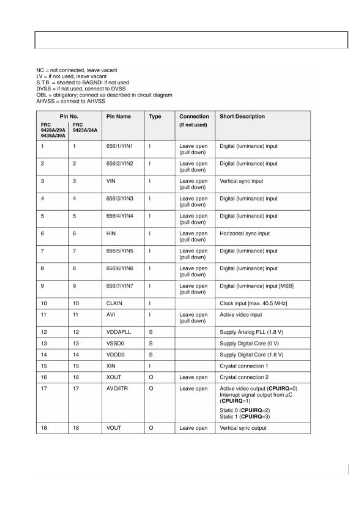
4-1) Pin Functions.
CIRCUIT DESCRIPTIONS
SERVICE MANUAL
PAGE:
50
Page 51
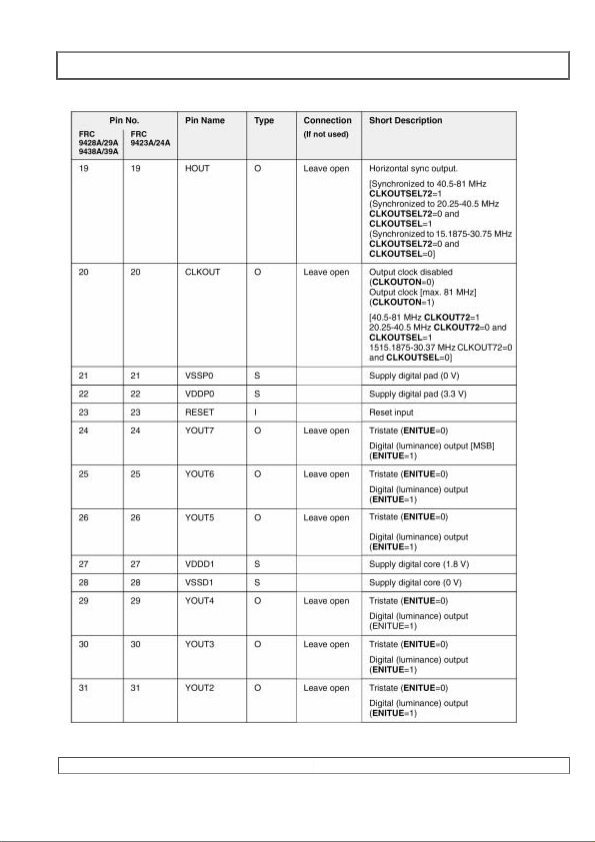
4-2) Pin Functions.
CIRCUIT DESCRIPTIONS
SERVICE MANUAL
PAGE:
51
Page 52
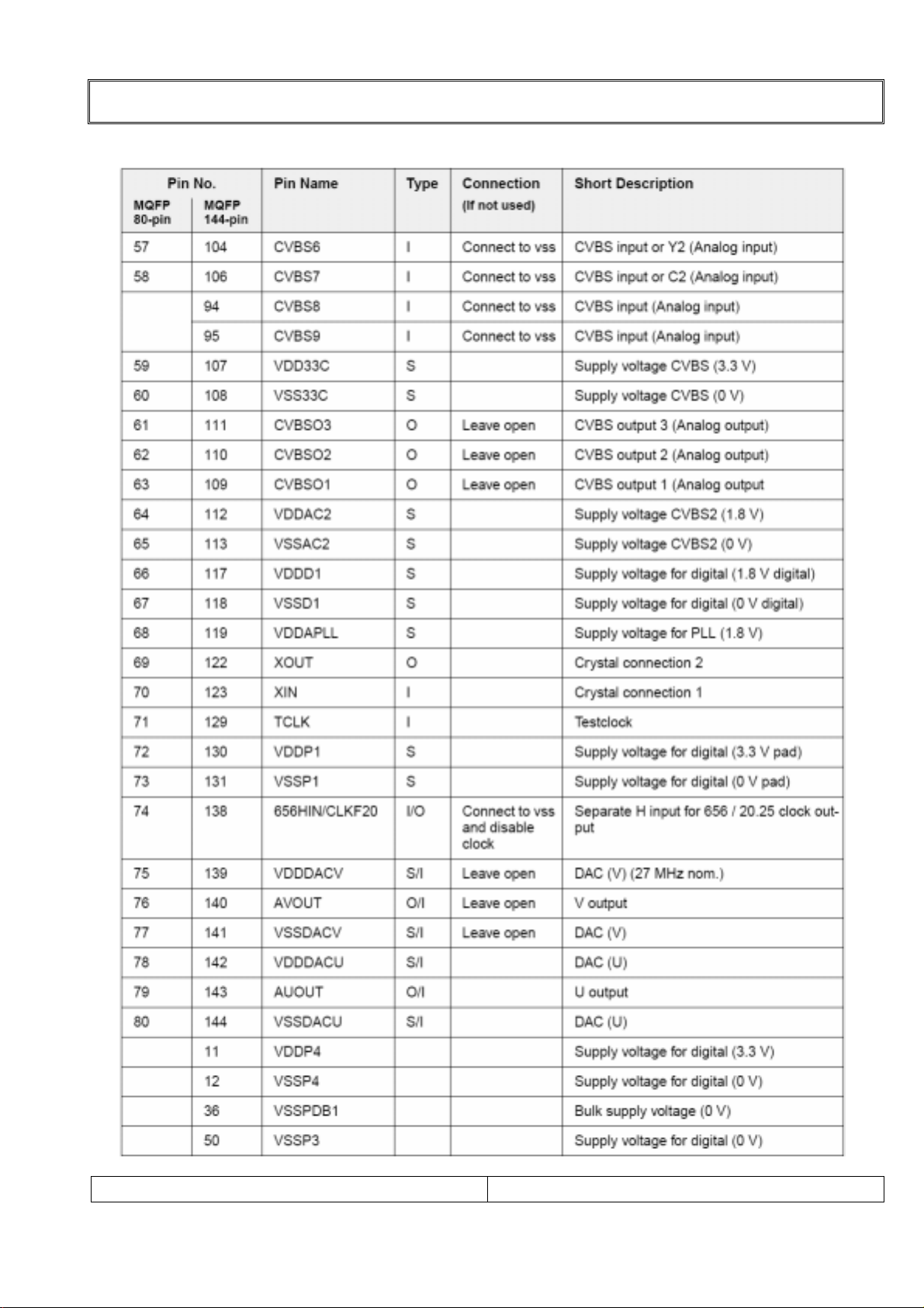
4-3) Pin Functions.
CIRCUIT DESCRIPTIONS
SERVICE MANUAL
PAGE:
52
Page 53
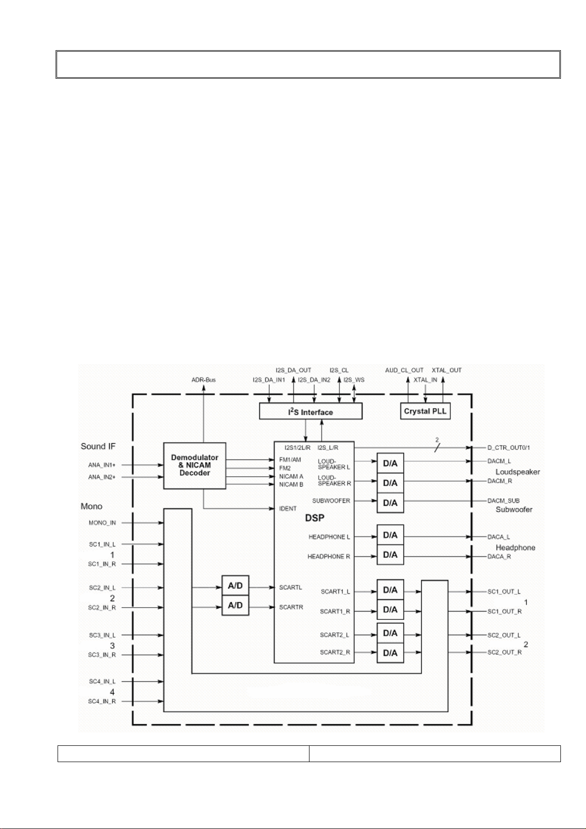
CIRCUIT DESCRIPTIONS
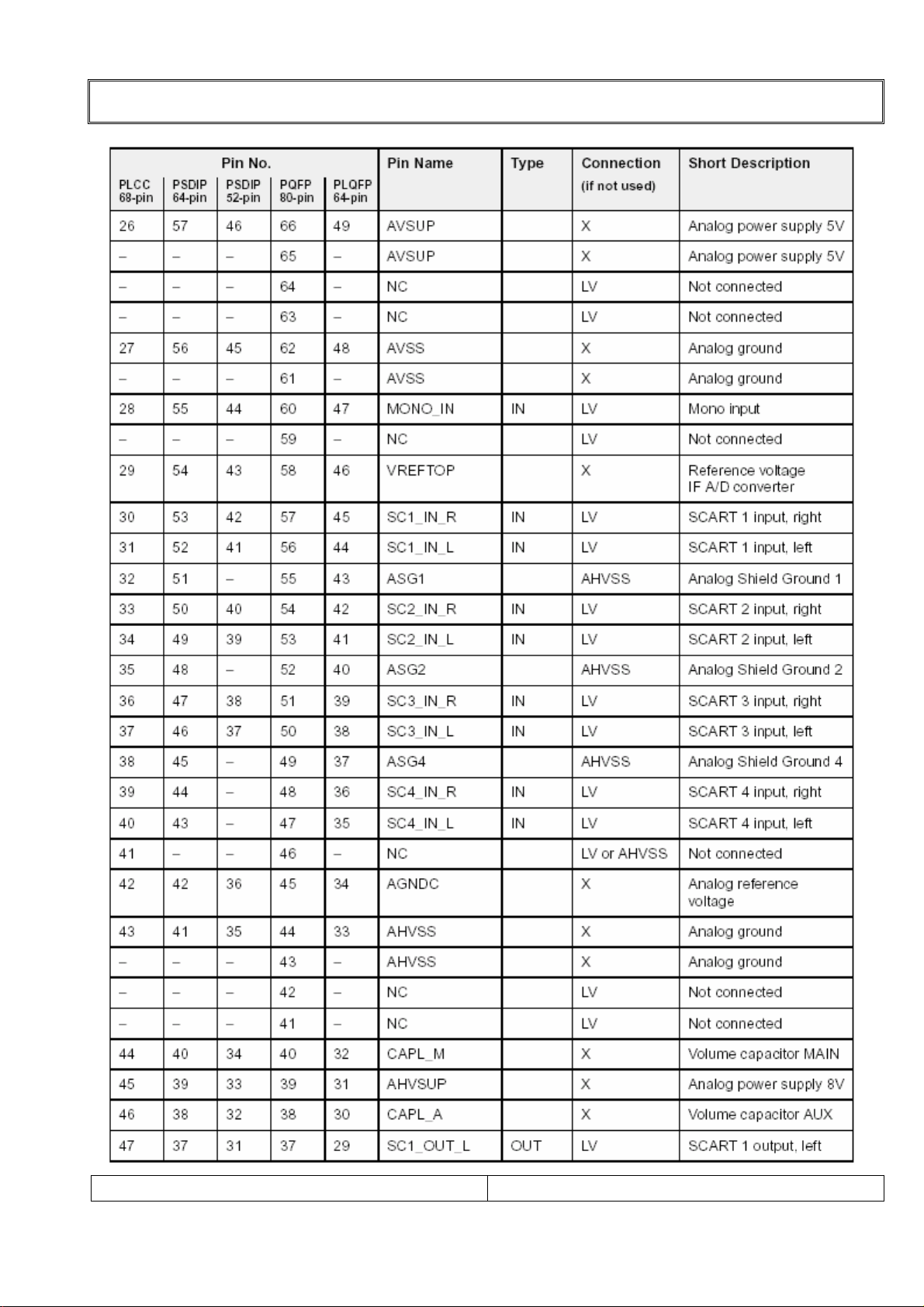
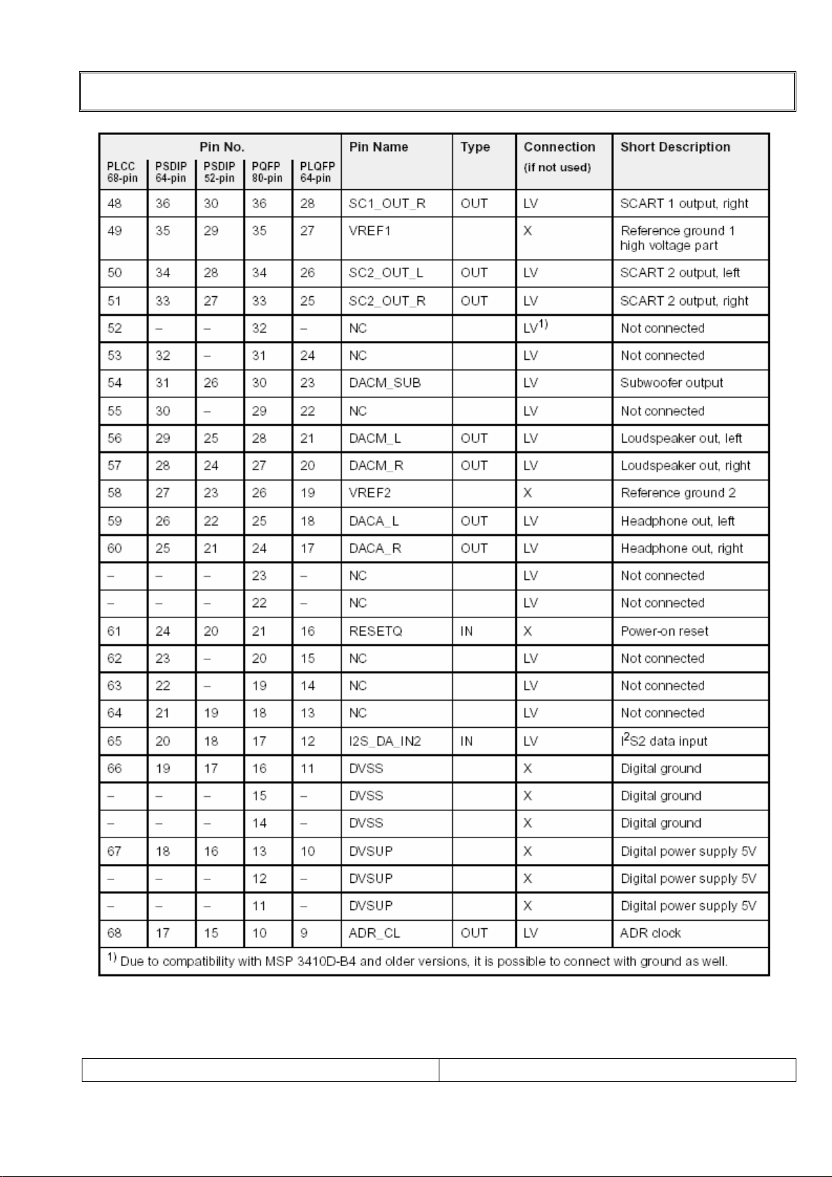
6. AUDIO PROCESSOR SECTION.
Device: MSP3410D.
Features: Integrated A/D converter for sound-IF inputs
Automatic Gain Control (AGC) for analog IF input
FM demodulation
1) Description
The MSP 3410D is designed to perform demodulation of FM or AM-Mono TV sound.
Alternatively, two-carrier FM systems according to the German or Korean terrestrial specs or
the satellite specs can be processed with the MSP 3410D.
Digital demodulation and decoding of NICAM-coded TV stereo sound, is done only by the MSP
3410.
The MSP 3410D offers a powerful feature to calculate the carrier field strength which can be
used for automatic standard detection (terrestrial) and search algorithms (satellite). The IC may
be used in TV sets, as well as in satellite tuners and video recorders. It offers profitable
multistandard capability, including the following advantages.
Fabricated in an advanced CMOS process, the MSP3410D is provided in a space-saving
80-lead PQFP surface-mount plastic package.
2) Block Diagram.
SERVICE MANUAL
PAGE:
53
Page 54
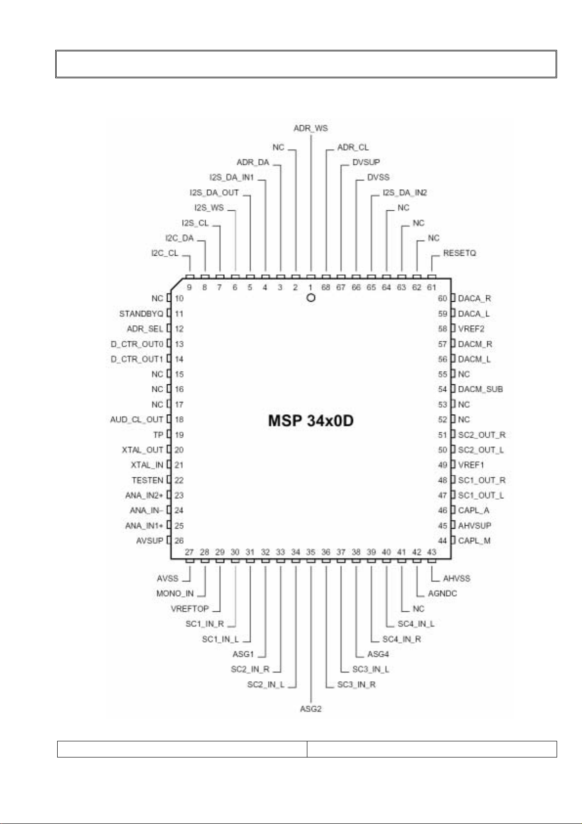
3) Pin configurations
CIRCUIT DESCRIPTIONS
SERVICE MANUAL
PAGE:
54
Page 55
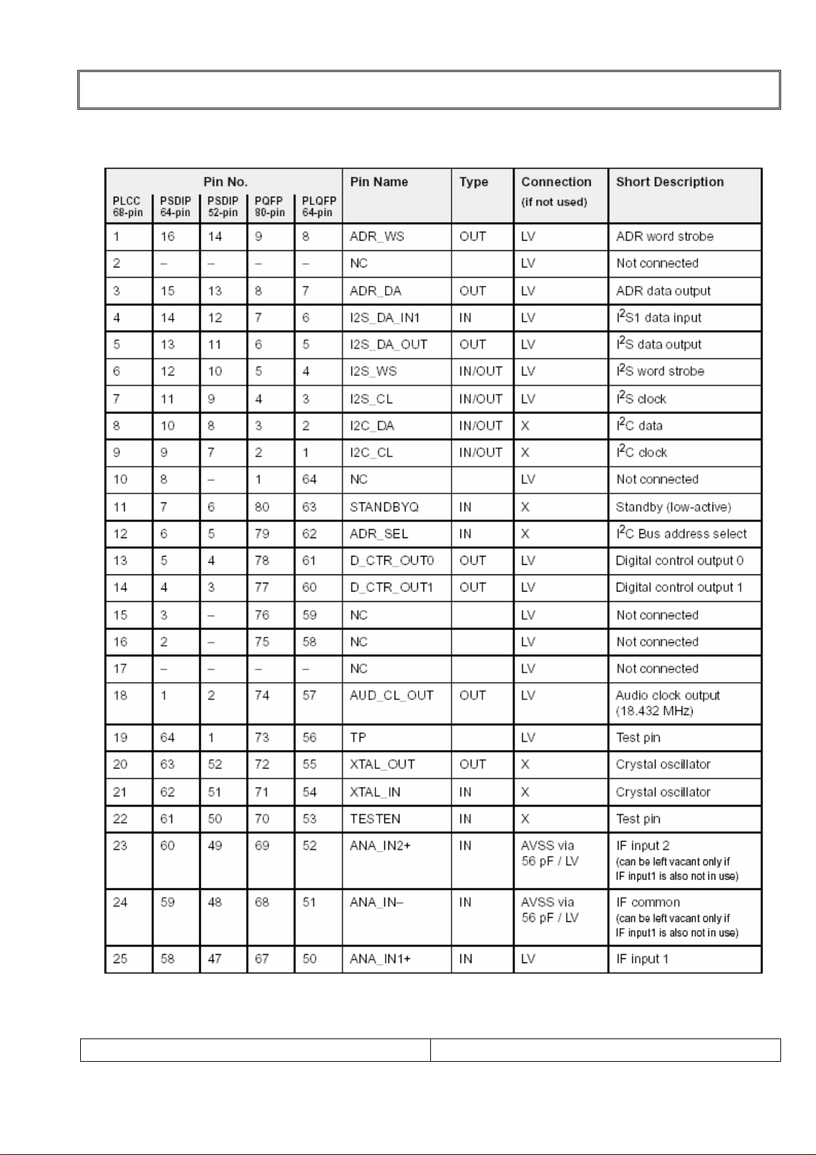
4) Pin Functions.
CIRCUIT DESCRIPTIONS
SERVICE MANUAL
PAGE:
55
Page 56
CIRCUIT DESCRIPTIONS
SERVICE MANUAL
PAGE:
56
Page 57
CIRCUIT DESCRIPTIONS
SERVICE MANUAL
PAGE:
57
Page 58
TROUBLE SHOOTING
SERVICE MANUAL
PAGE:
58
Page 59
TROUBLE SHOOTING
SERVICE MANUAL
PAGE:
59
Page 60
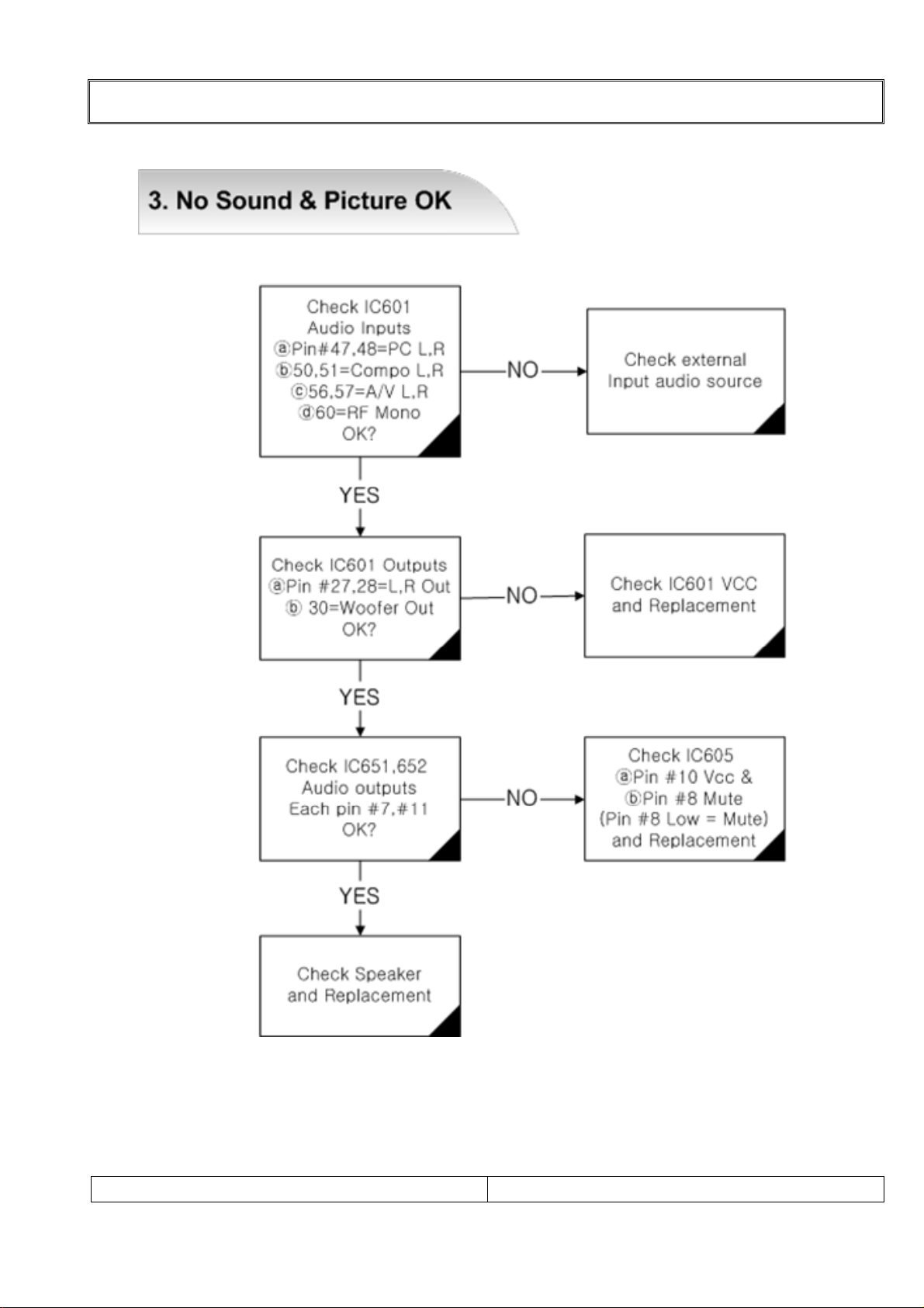
TROUBLE SHOOTING
SERVICE MANUAL
PAGE:
60
Page 61
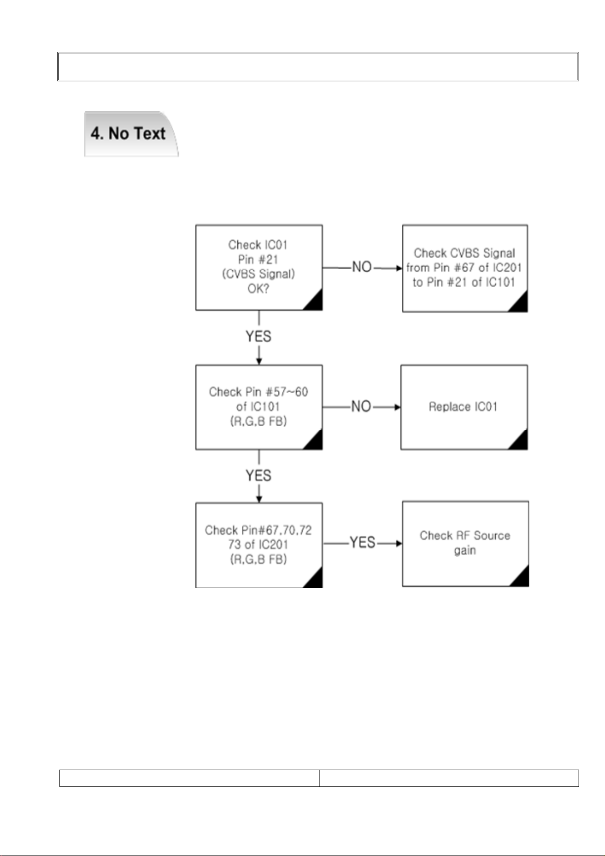
TROUBLE SHOOTING
SERVICE MANUAL
PAGE:
61
Page 62
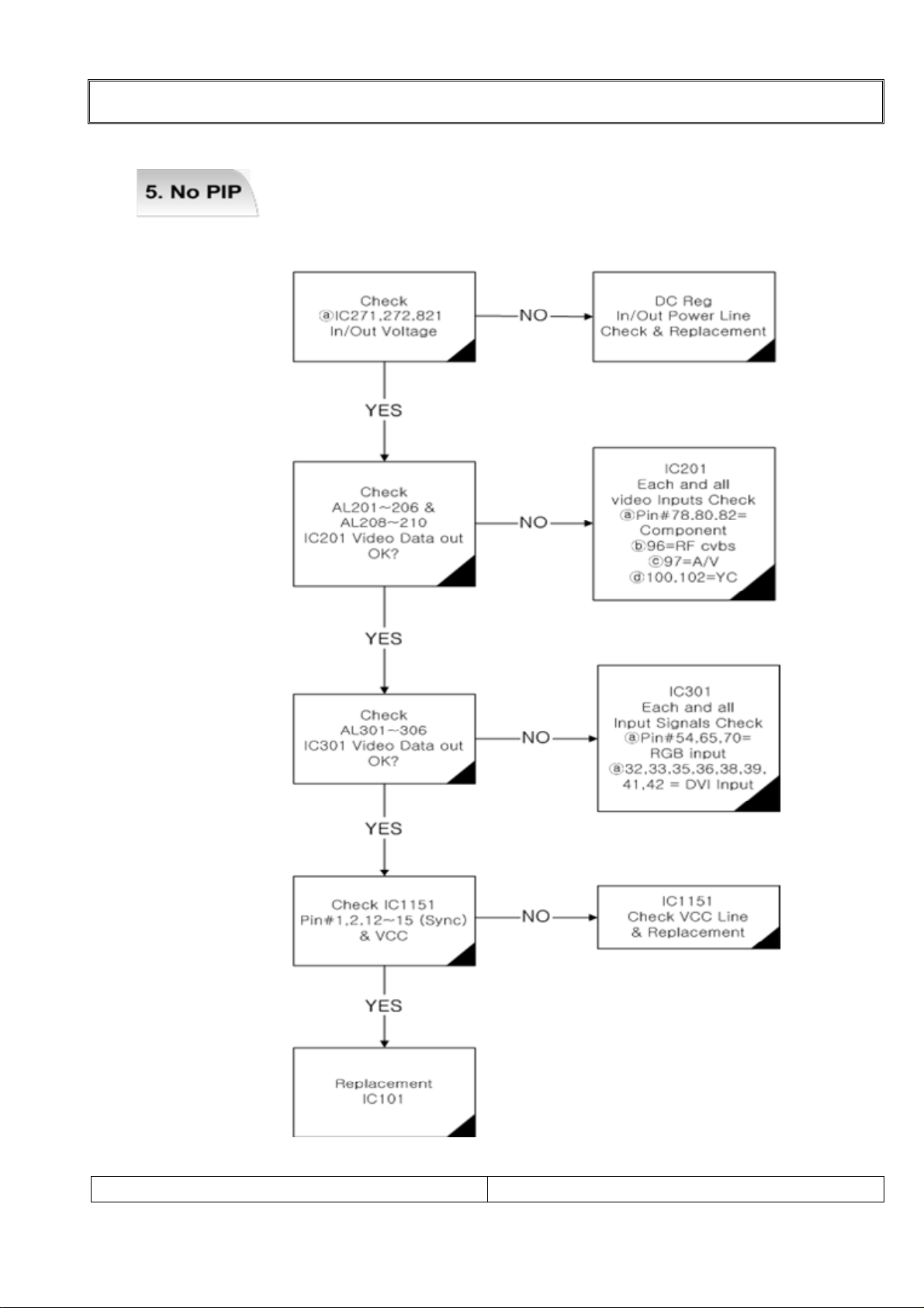
TROUBLE SHOOTING
SERVICE MANUAL
PAGE:
62
Page 63
WIRE DRESSING
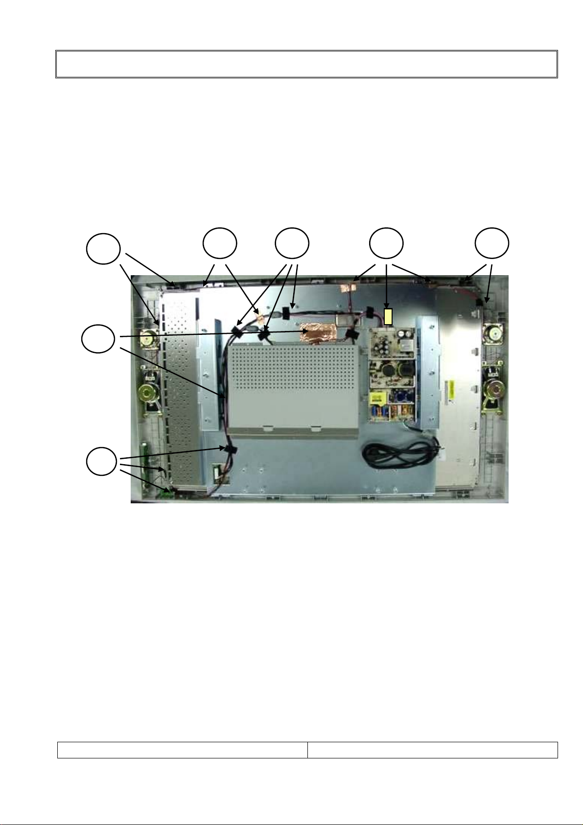
1. Wire Dressing
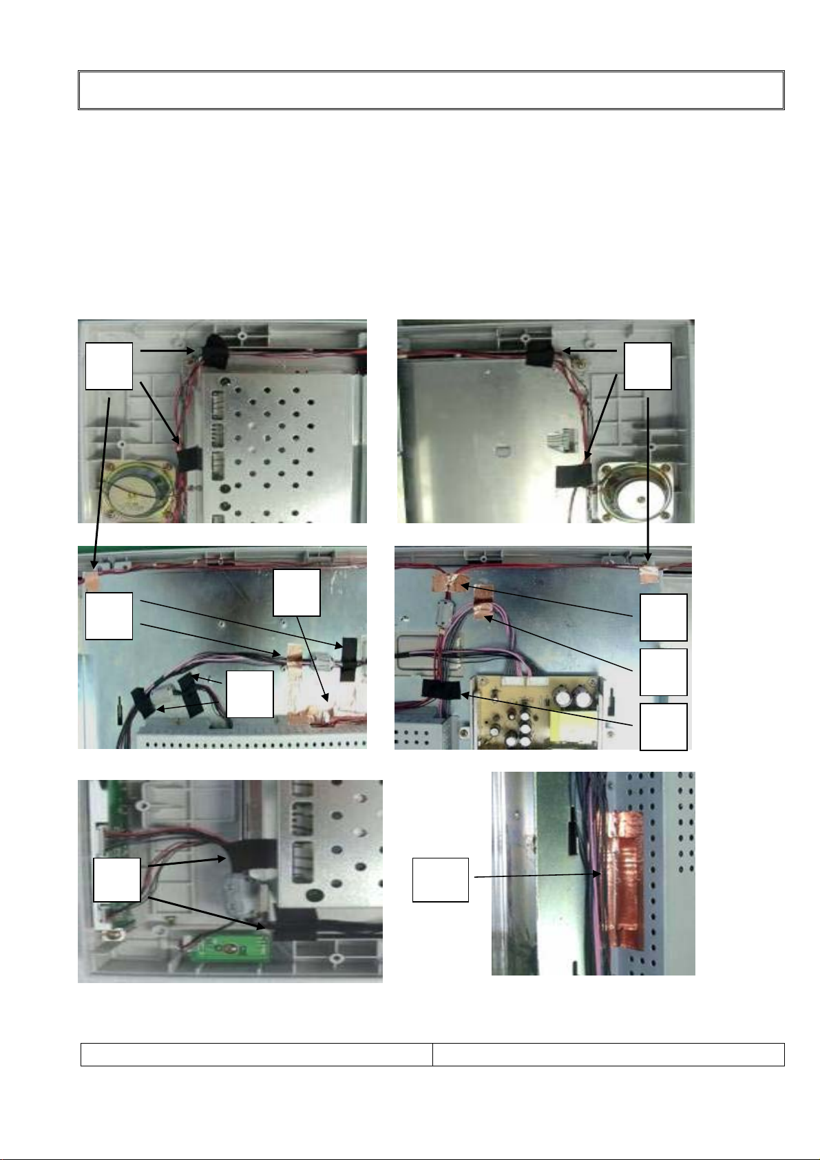
Note: Using acetate Tape Î No1,No3,No5, No7.
Using Copper Tape Î No2, No4. (Conducted tape)
Using Copper Tape Î No6. (Conducted tape)
Unit : mm
5
4 2 1
3
6
7
SERVICE MANUAL
PAGE:
63
Page 64
WIRE DRESSING
1) Wire Dressing for Left main speaker & sub speaker. ( No.1)
2) Wire Dressing for Right main speaker & sub speaker. ( No.2 )
3) Wire Dressing for Inverter ( No.3)
4) Wire Dressing for Key control & Inverter. ( No.4)
5) Wire Dressing for LVDS. ( No.5 )
6) Wire Dressing for Left / Right main speaker & sub speaker .( No.6 )
7) Wire Dressing for Main Power. ( No.7 )
8) Wire Dressing for Main Power & main/sub Speaker. ( No.8 )
9) Wire Dressing for Key control & IR. (NO 9)
10) Rear Shield Hole. (NO 10)
1 2
5
3
6
7
4
8
9
SERVICE MANUAL
10
PAGE:
64
Page 65
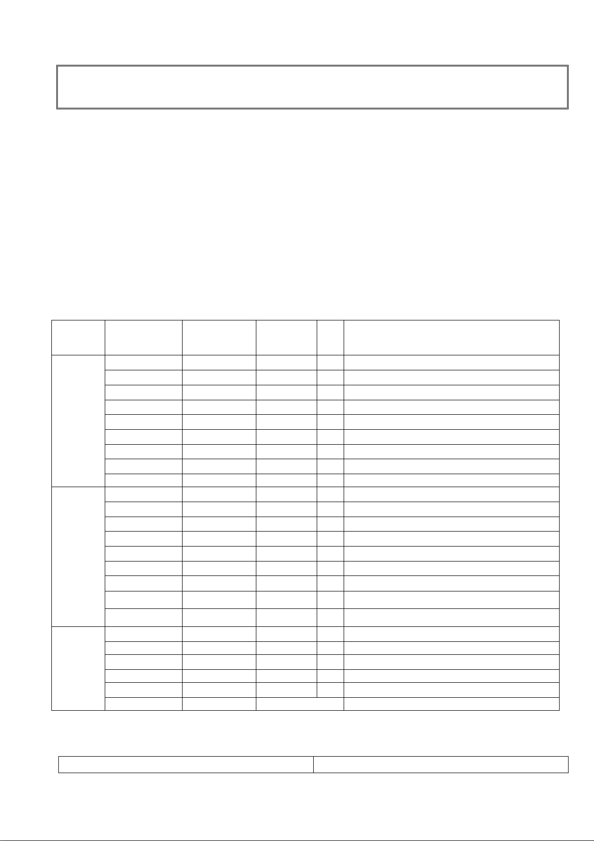
ADJUSTMENT INSTRUCTION
WITH DEFAULT FACTORY DATA
1.SVC mode data Adjustment
NOTE!! When the EEPROM has been replaced, the SVC data should be restored as the
function of individual system and specification.
[ Enter and exit SVC mode ]
Note: into the SVC mode, Initialize with default data.
1) Press 5 Seconds MENU buttons on both TV set and Remote Controller at the same
time to get into SVC mode.
2) Press the Yellow button several times to find SVC Data.
3) Input the corresponding SVC data referring to Table below with the Volume Up/down
key.
4) Press the OK button to memorize the data.
5) Press TV/AV button to exit SVC mode
2-1. Factory outgoing setting & Initialize with default data (into the SVC mode).
PAGE ITEM
outgoing
setting
AGC
RD
DATA 1
GD
BD
RO
GO
BO
PC CP
50 PR * 1 * means current program NO.
DCI
DATA0
DATA1
DATA2
DATA 2
DATA3
DATA4
DATA5
DATA6
Factory
15 15
127 127
127 127
127 127
79 79
79 79
79 79
5 5
0 0
255 255
255
255
255
255
255
255
255
255
255
255
255
255
Initialize
with default
data
REMARK
Ex
Variable Data(0-31)
PC Contrast Coefficient-RED(0-255)
PC Contrast Coefficient-GREEN(0-255)
PC Contrast Coefficient-BLUE(0-255)
PC Brightness Coefficient-RED(0-63)
PC Brightness Coefficient-GREEN(0-63)
PC Brightness Coefficient-BLUE(0-63)
PC Charge Pump(0-7)
Variable Data(0-1)
Variable Data(0-255)
Variable Data(0-255)
Variable Data(0-255)
Variable Data(0-255)
Variable Data(0-255)
Variable Data(0-255)
Variable Data(0-255)
DATA 3
DATA7
FP
255
255
52 52
NP 122 122
SP
63 63
S1 VOL 44 44
S2 VOL
44 44
Variable Data(0-255)
FM Prescaler (0-127)
NICAM Prescaler (0-127)
Scart Prescaler (0-127)
Scart1 Prescaler (0-127)
Scart2 Prescaler (0-127)
50 PR * 1 * means current program NO.
SERVICE MANUAL
PAGE:
65
Page 66
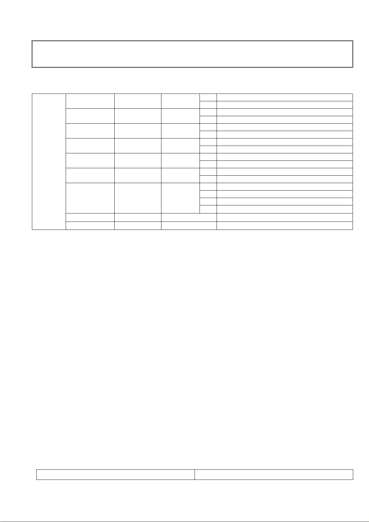
2-2.SVC Data Table
200PR 0 0
TEXT 1 1
TOP 1 1
SCART 1 1
DATA 4
ACMS 1 1
CH+AU 0 0
SYS 1 1
50 PR * 1
121 Opt 1
ADJUSTMENT INSTRUCTION
WITH DEFAULT FACTORY DATA
0 100PR
1 200PR
0 Not apply to TEXT
1 Apply to TEXT
0 TELETEXT TOP OFF
1 TELETEXT TOP ON
0 Apply to COMPONENT
1 Apply to SCART
0 Not apply to ACMS
1 Apply to ACMS
0 Used except for CHINESS or AUSTRALIA
1 Used CHINESS or AUSTRALIA
0 BG/I/DK
1 BG/I/DK/L
2 BG/I/DK/M
3
* means current program NO.
Translate HEX into DEC(DATA3VALUE1)
RESERVED
SERVICE MANUAL
PAGE:
66
Page 67
ADJUSTMENT INSTRUCTION
WITH DEFAULT FACTORY DATA
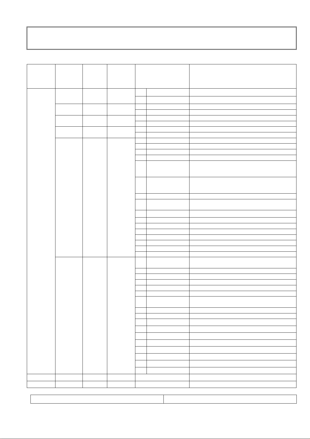
2-3.SVC Data Table
Factory
PAGE ITEM
outgoing
setting
DUAL 0 0
MONO 0 0
A2 ST 1 1
VOL 1 1
LANG 1 1
DATA 5
T-LAN 0 0
50 PR *
57 Opt 2
Initialize
with
default
data
0
1
0 Not apply to MONO option
1 Apply to MONO option
0 Not apply to NICAM STEREO option
1 Apply to NICAM STEREO option
0 Sound curve option 1
1 Sound curve option 2
0 ENG ONLY ENGLISH ONLY
1 EU-5EA ENGLISH/GERMAN/FRANCE/ITALY/SPAIN
2 EU CIS EU-5EA + CIS
3 E+CHINA ENGLISH + CHINESS(RUSSIA)
4 EU-12EA
5
6 YAHOO YAHOO
7 EU-6EA
8 KOREA
9 JAPAN ONLY SELECT JAPAN
10 USA ENGLISH/FRANCE/SPAIN/NETHERLANDS
11 S-AMERICA ENGLISH / PORTUGAL/ SPAIN
12 NTSC ENG ENGLISH
13 RESERVED ENGLISH
14 RESERVED ENGLISH
15 RESERVED ENGLISH
0 WEST EU
1 EAST EU1 POLAND/SLOVENIA/ROMANIA etc
2 TURKEY EU TURKEY
3 EAST EU2 HUNGRY/SERVIA
4 CYRILLIC1 ESTONIA
5 CYRILLIC2 ESTONIA
6 CYRILLIC3
7 TURK GRE1
8 TURK GRE2
9 TURK GRE3
10 ARAB ERA
11 ARAB ENG
12 ARAB HEB1
13 ARAB HEB2
14 FARS ENG
15 FARS FRA
16 FABS ALL
Ex REMARK
Not apply to DUAL option
Apply to DUAL option
English,German, FRANCE/ITALY/SPAIN,
Netherland,Sweden,Norway,Denmark,Finlandi,
Portugal, Rumania
N EU 06EA
(N EU 12EA)
English , Netherland, Sweden,Norway,Denmark,
Finland, Portugal, Rumania, Israel, Hungary,
Czech, Russian
ENGLISH / GERMAN / FRANCE / ITALY/SPAIN
/ Netherland
ENGLISH / KOREA
WESTEU/U.K/GERMAN/FRANCE/ITALY/
SPAIN/SWEDEN/CZECH Rep./NORWAY etc
RUSIA/UKRAINE/ESTONIA/CROATIA/KAZAKH
STAN
TURKEY/GREECE
ARAB CULTURE(EMIRATES U.A.E)
ARAB/HEBREW
PARSI
-
-
* means current program NO.
Translate HEX into DEC(DATA4)
SERVICE MANUAL
PAGE:
67
Page 68
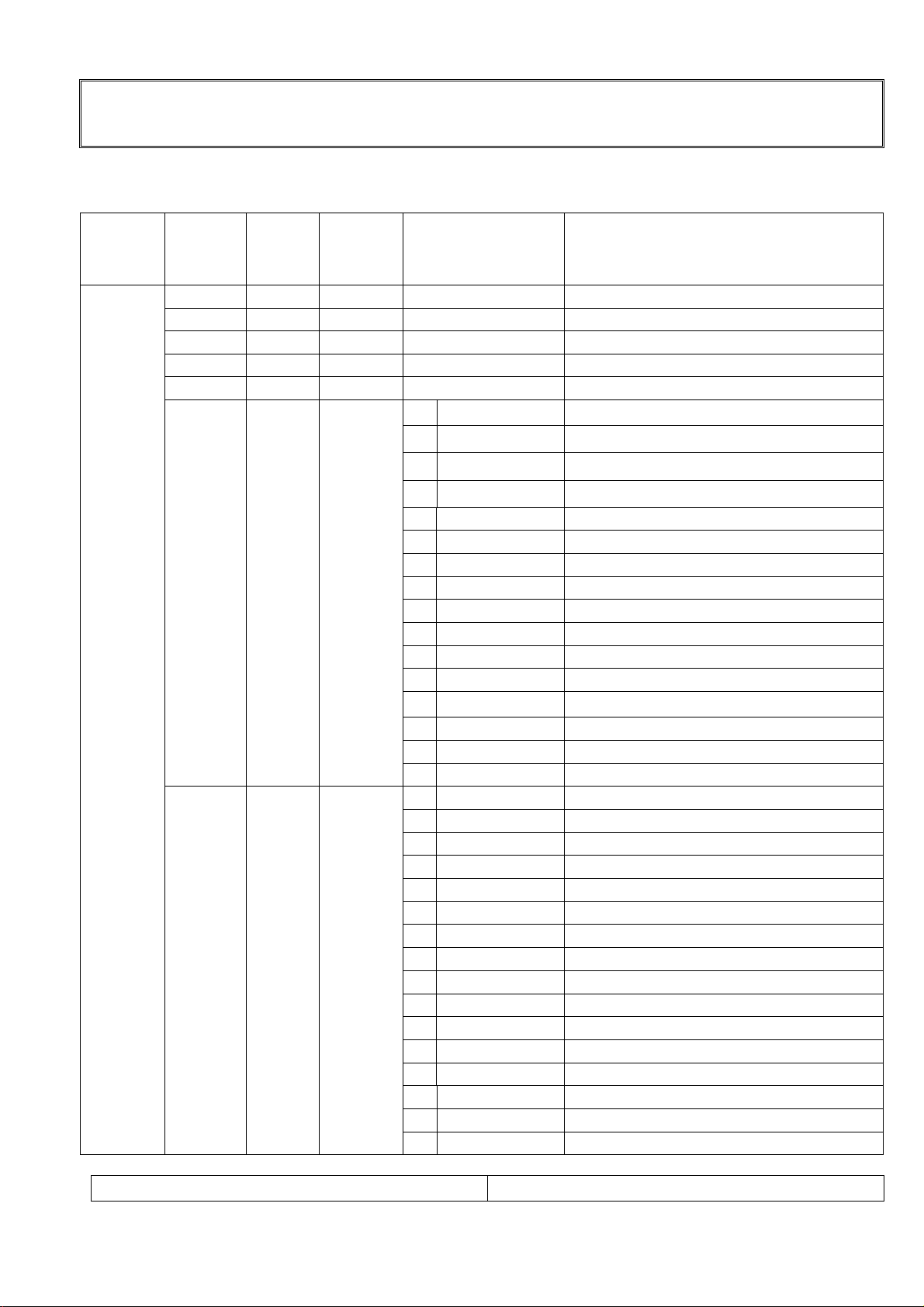
2-4. SVC Data Table
PAGE ITEM
FVS
DVI
D-TV
VCHIP
WOFER
PANEL 0 0
DATA 6
RESET 15 15
ADJUSTMENT INSTRUCTION
WITH DEFAULT FACTORY DATA
Factory
outgoing
setting
1
1
0
0
1
Initialize
with
default
data
1
1
0
0
1
0
1
2
3
4
5
6
7
8
9
10
11
12
13
14
15
0
1
2
3
4
5
6
7
8
9
10
11
12
13
14
15
Ex REMARK
SS-40 L01
SS-40 L02
SS-42
LG-46
RESERVED
RESERVED
RESERVED
Frequency voltage Disable/Enable(0-1)
Fix (All Model application)
D-TV Disable/Enable (0-1)
Violence Disable/Enable (0-1)
Fix (All Model application)
Used SS-40 L01 PANEL
Used SS-40 L02 PANEL
Used SS-42 PANEL
Used LG-46 PANEL
RESERVED
RESERVED
RESERVED
RESERVED
RESERVED
RESERVED
RESERVED
RESERVED
RESERVED
NEC-A
Marantz
L-Model
E-Model
M-Model
KOREA
USA
Save NEC-A TV Channel
Save Marantz TV Channel
Save L-Model TV Channel
Save E-Model TV Channel
Save M-Model TV Channel
Save KOREA TV Channel
Save USA TV Channel
RESERVED
RESERVED
RESERVED
RESERVED
RESERVED
RESERVED
RESERVED
RESERVED
RESERVED
SERVICE MANUAL
PAGE:
68
Page 69
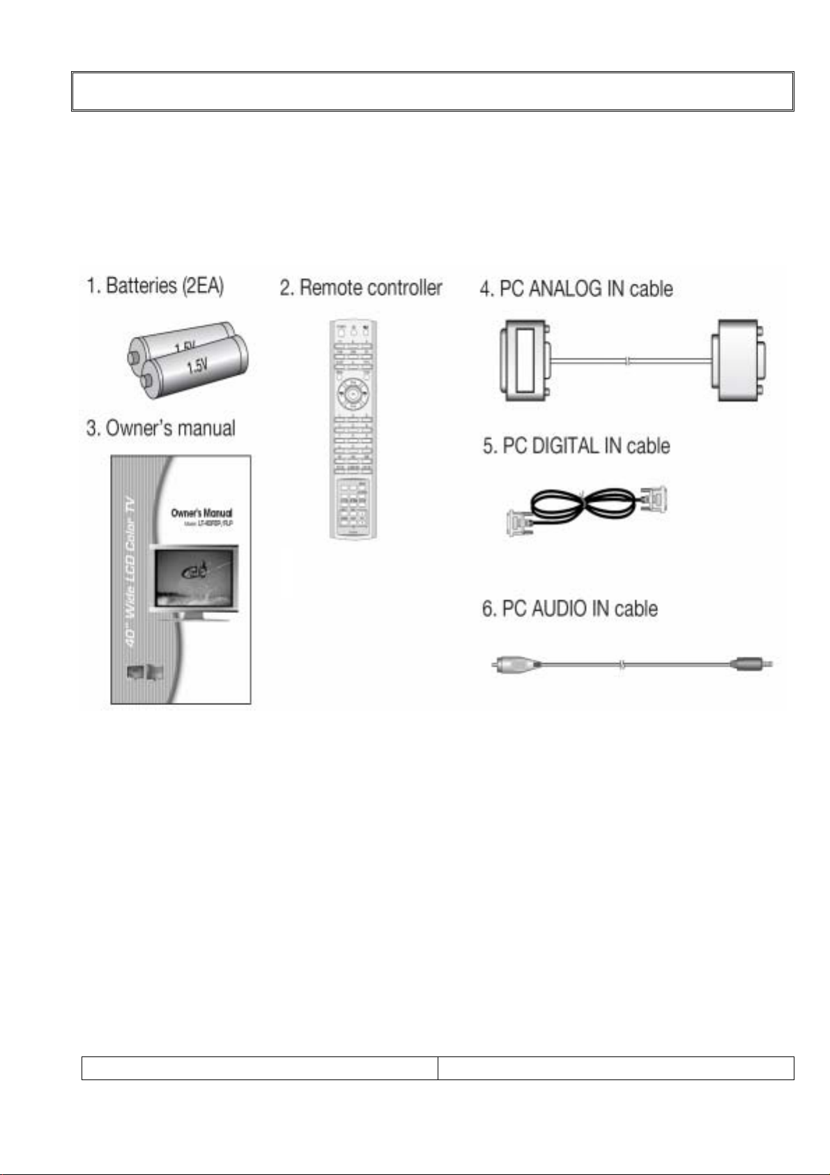
INSPECTION INSTRUCTION
1. Supplied Accessories
Note: Make Sure the following accessories are provided with Product.
SERVICE MANUAL
PAGE:
69
Page 70
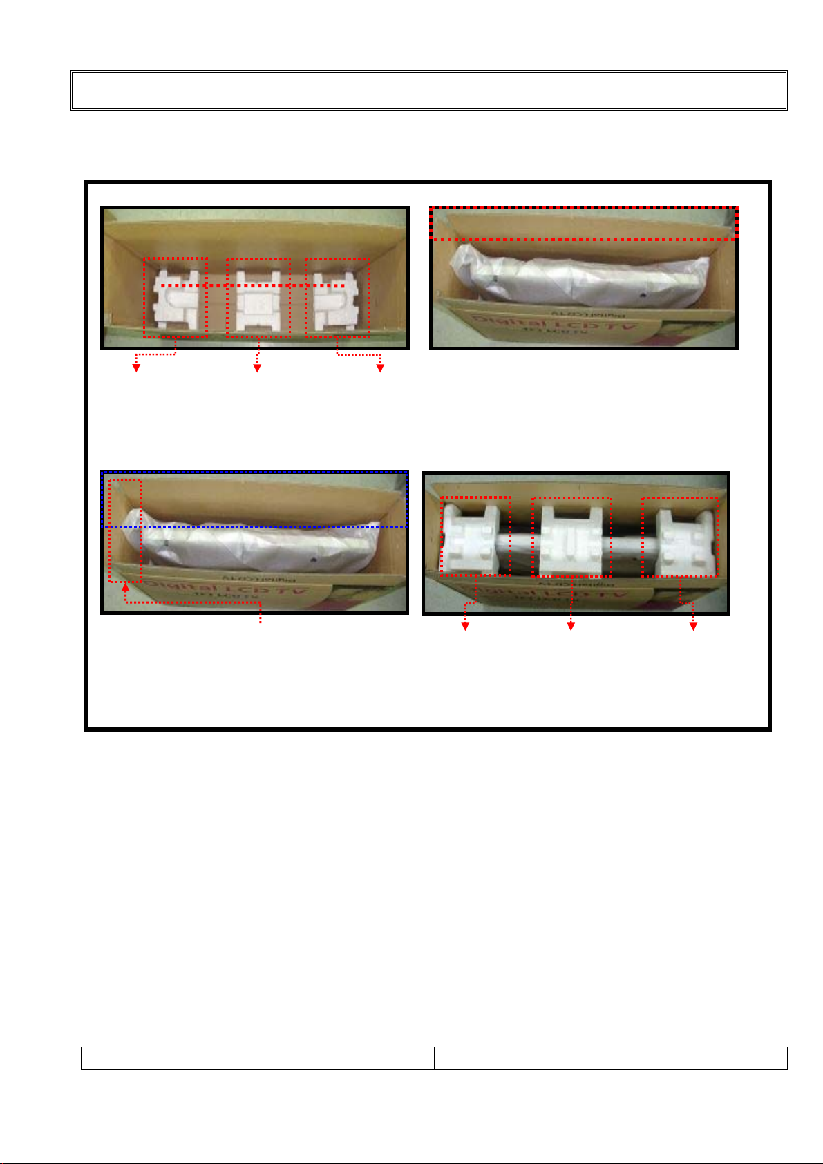
2. Packing condition
INSPECTION INSTRUCTION
SET FRONT
PACKING FRONT
PACKING
BOTTOM “L”
<picture 1> PACKING insert in BOX
PACKING
BOTTOM “M”
SET FRONT
BOX FRONT
SET FRONT
<picture2> SET insert in BOX
PACKING
BOTTOM “R”
SET FRONT
Insert position for the ACCESSORY BOX
<picture3> Accessory Box insert
PACKING
TOP “L”
<picture4> TOP PACKING insert in BOX
PACKING
TOP “M”
PACKING
TOP “R”
SERVICE MANUAL
PAGE:
70
Page 71
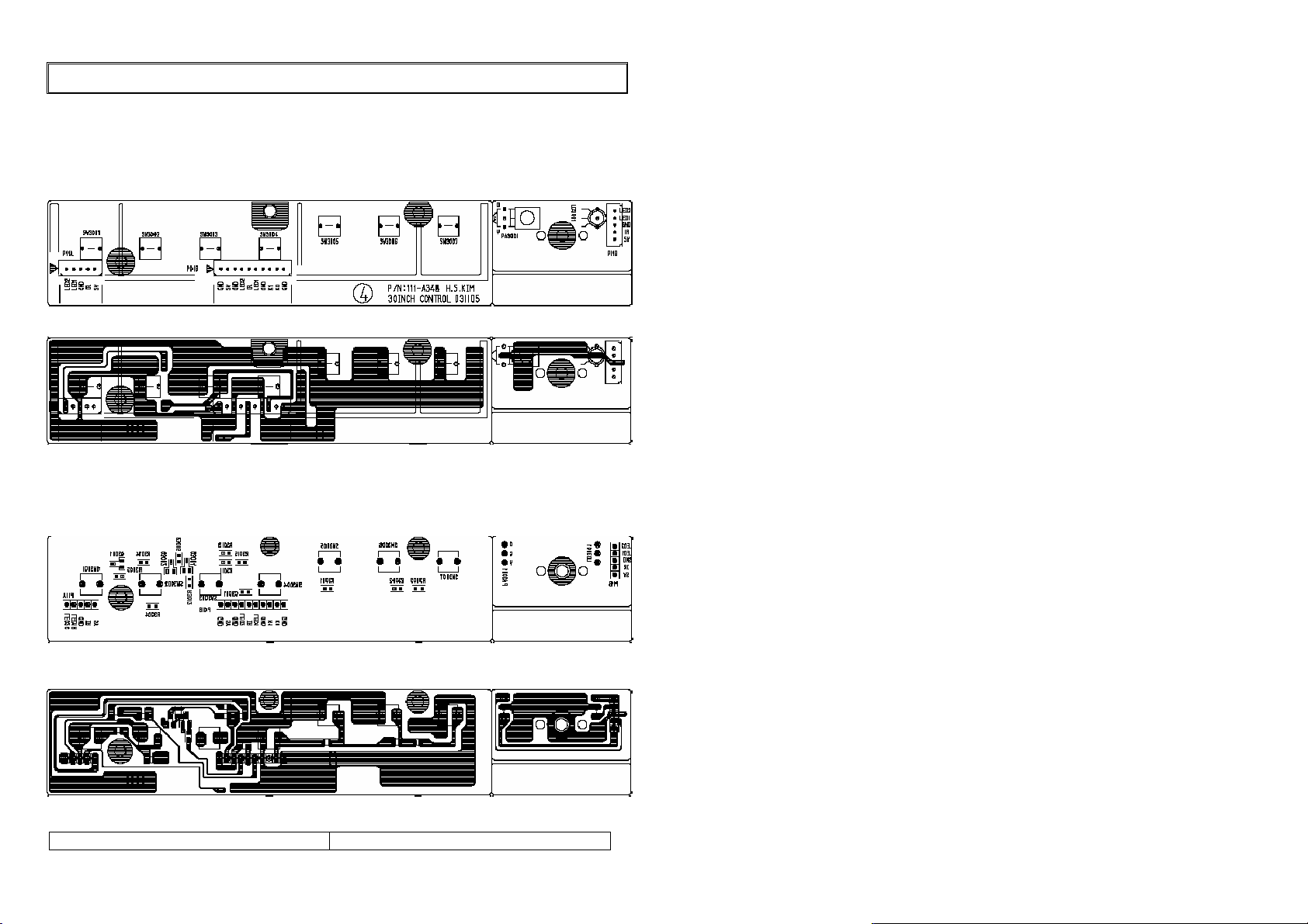
3-1. CONTROL PCB
1 ) TOP
< COMP >
PCB LAYOUT
< PATTERN >
2) BOTTOM
< COMP >
< PATTERN >
SERVICE MANUAL
PAG E:
71
Page 72
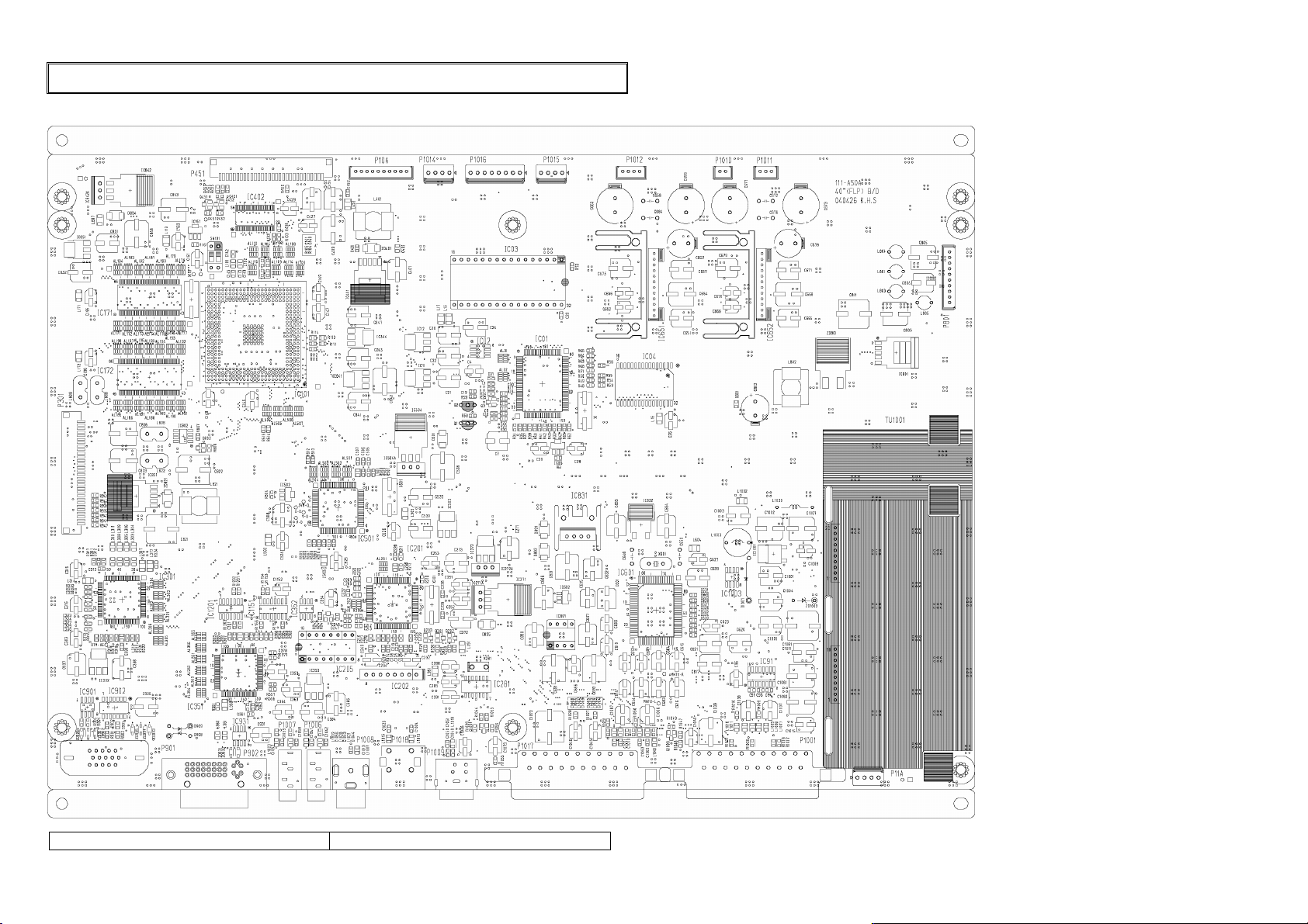
3-1. Main PCB ( TOP COMP )
PCB LAYOUT
SERVICE MANUAL
PAG E:
72
Page 73
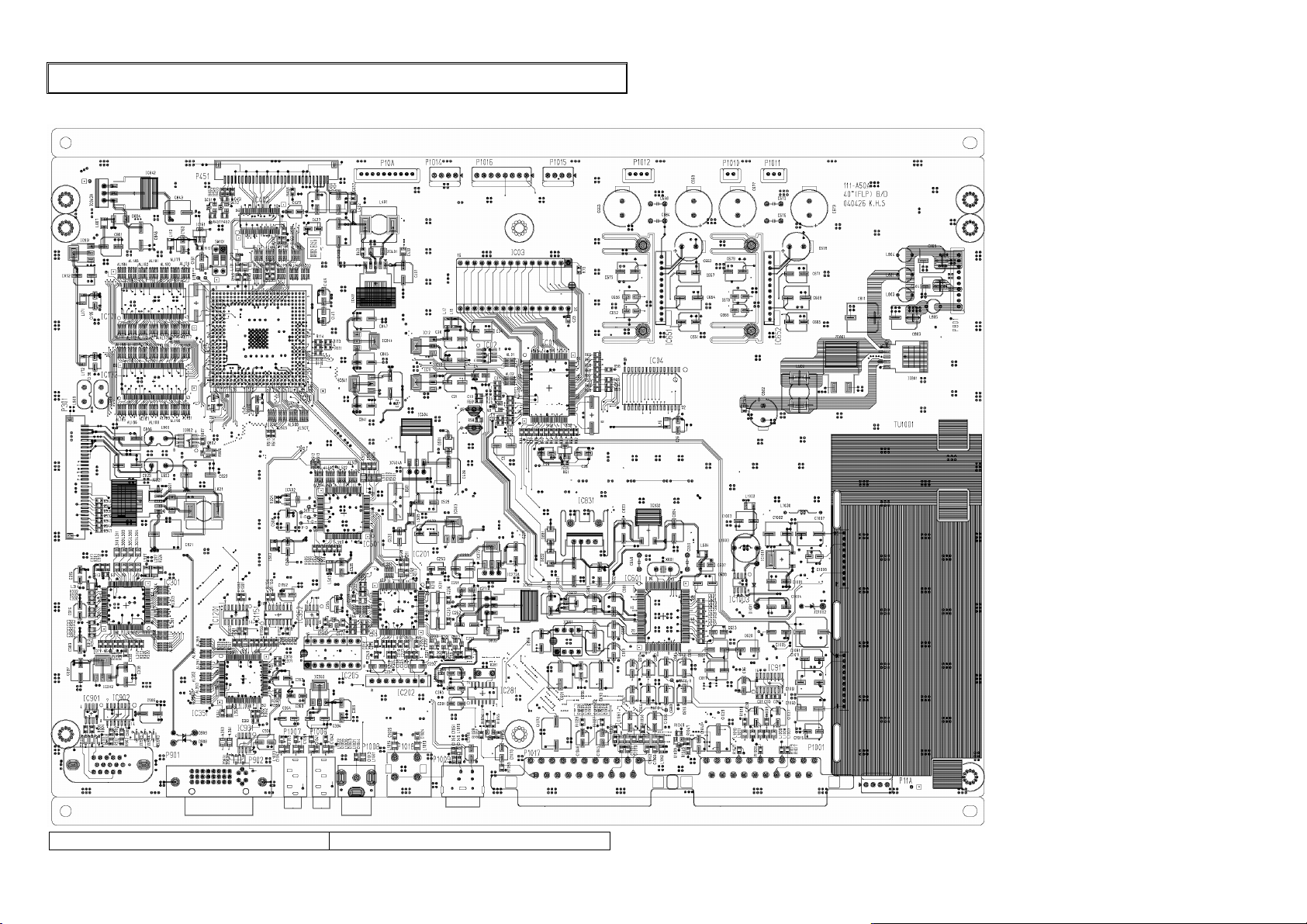
3-2. Main PCB (TOP PATTEN)
PCB LAYOUT
SERVICE MANUAL
PAG E:
73
Page 74
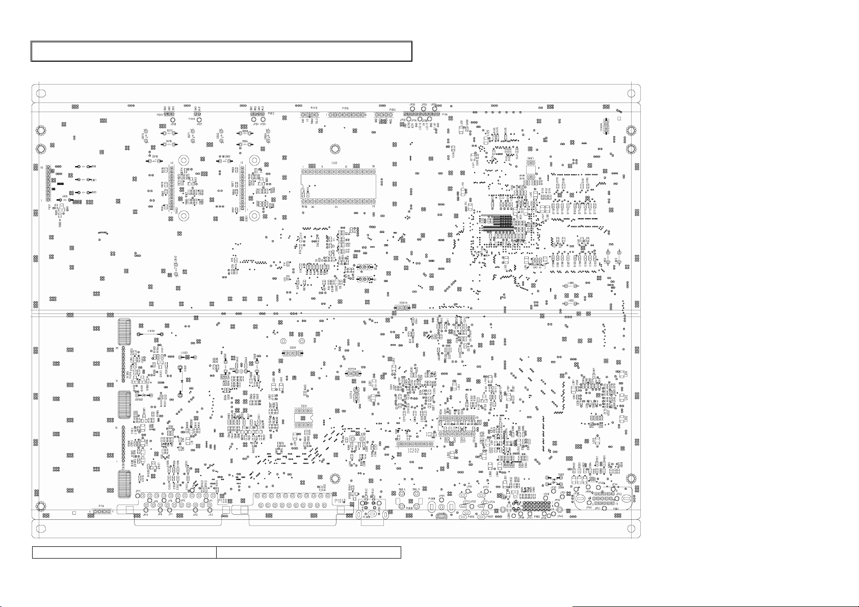
3-3. Main PCB ( BOTTOM COMP )
PCB LAYOUT
SERVICE MANUAL
PAG E:
74
Page 75
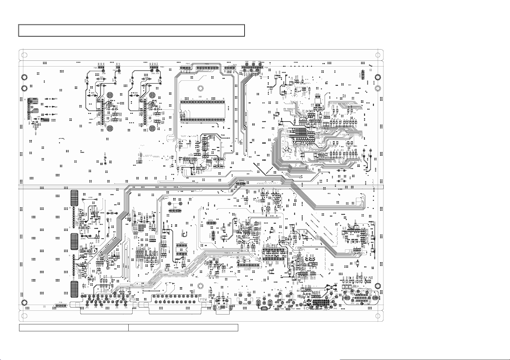
3-4. Main PCB ( BOTTOM PATTEN)
PCB LAYOUT
SERVICE MANUAL
PAG E:
75
Page 76
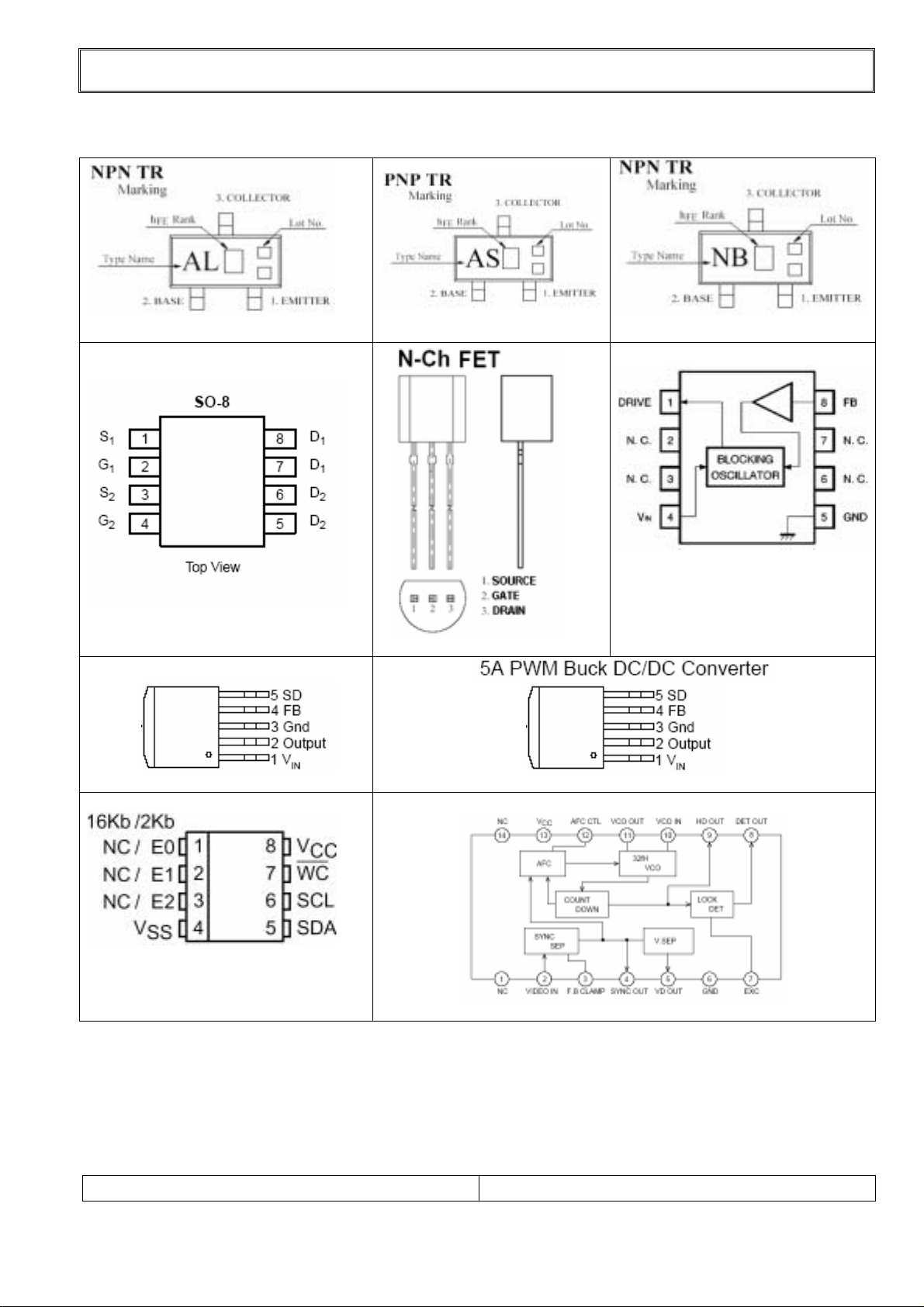
1-1. Part appearance
PART APPEARANCE
C3875S
DUAL P-CH 30V MOSFET
SI4925DY
3A REGULATOR
A1504S
2N7000
C102S
RegulatorforTuningVoltage
BA6161F
AP1501 ( 5V )
AP1501A ( 12V & 5V )
Sync-signal separator with AFC and Sync detector
EEPROM24C16W,24C02W
LA7217
SERVICE MANUAL
PAGE:
76
Page 77
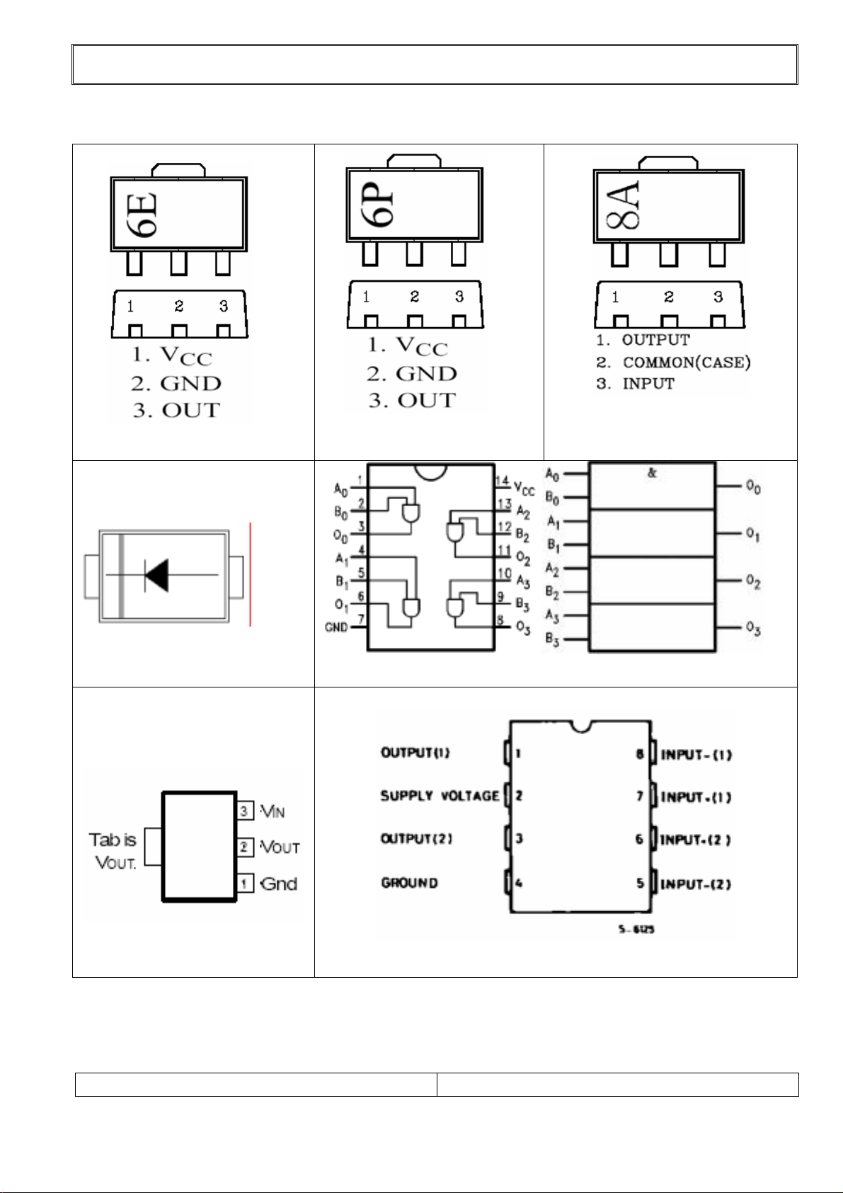
1-2. Part appearance
VoltageDetector
KIA7027AF
PART APPEARANCE
VoltageDetector
KIA7042AF
Voltage Reg
KIA78L05F
Schottky Rectifier B340
VOLTAGE
REGULATOR - 1A
IRU-1010 (1.8V / 2.5V /3.3V)
TTL LOGIC IC 74F08
DUAL LOW VOLTAGE POWER AMPLIFIER ( MINIDIP)
TDA2822
SERVICE MANUAL
PAGE:
77
Page 78
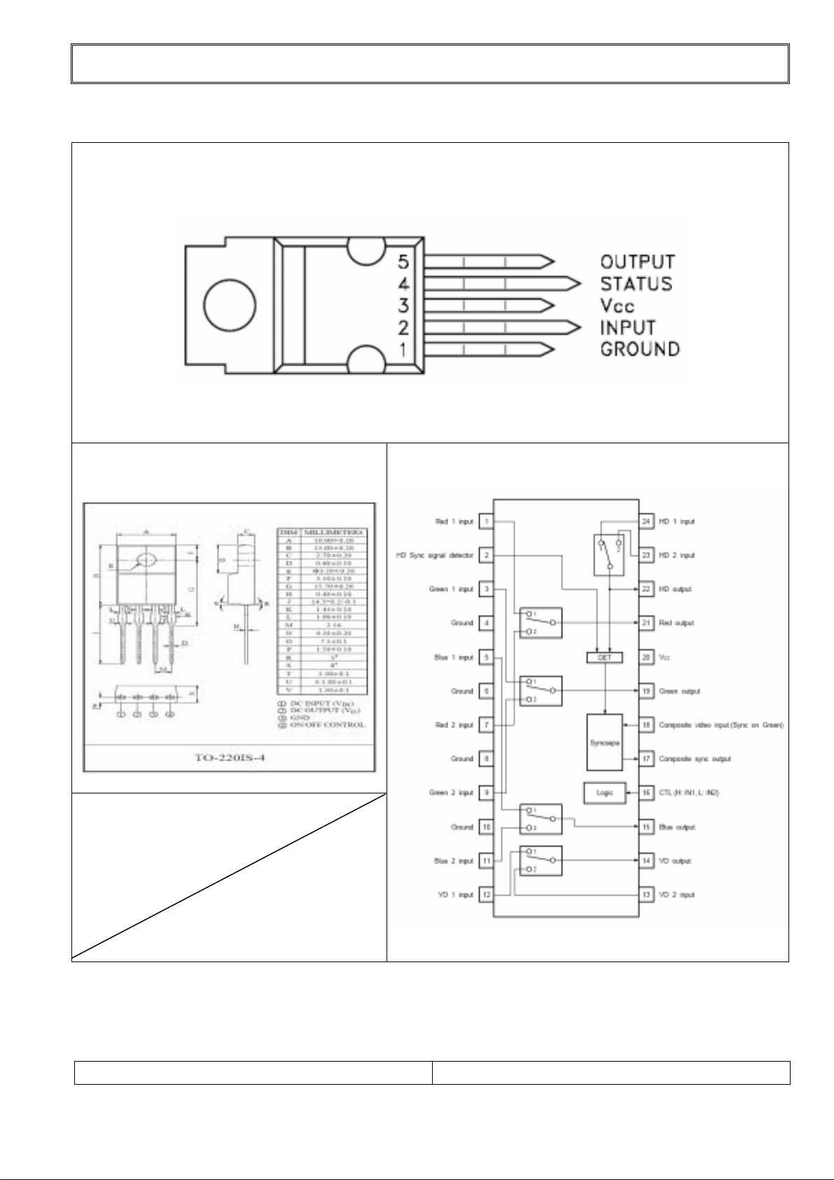
1-3. Part appearance
VOLTALGE REGULATOR
PART APPEARANCE
HIGH SIDE SMART POWER SOLID STATE RELAY
VERTICAL
VN02AN
INPUT SELECTOR SWITCH FOR HIGH
DEFINITION DISPLAY
A78R08(8V)
BA7657F
SERVICE MANUAL
PAGE:
78
Page 79
REPLACEMENT PART LIST
1.Parts List (Assemble process)
LEVEL
1
1
1
1
1
1
1
1
1
1
1
1
1
1
1
1
1
1
1
1
1
1
1
1
1
1
1
1
1
1
1
1
1
1
1
1
1
1
1
1
1
1
1
1
1
1
PART NO PART NAME DESCRIPTION Q,TY
300-003R 40 ACCESSORY BOX BOX, ACCESSORY 1
300-018B 40,COLOR,NO BRAND BOX, GIFT 1
310-016A 40",F-MODEL,TOP-L PACKING, TOP "L" 1
310-016B 40",F-MODEL,TOP-M PACKING, TOP "M" 1
310-016C 40",F-MODEL,TOP-R PACKING, TOP "R" 1
310-016D 40",F-MODEL,BOTTOM-L PACKING, BOTTOM "L" 1
310-016E 40",F-MODEL,BOTTOM-M PACKING, BOTTOM "M" 1
310-016F 40",F-MODEL,BOTTOM-R PACKING, BOTTOM "R" 1
320-001A ACCESSORY PACKING BAG, VINYL 1
321-009A 40 SET PACKING BAG, PACKING 1
402-004Z 40 POWER CORD HOLDE CORD HOLDER 1
404-004A F/N, L/KEY,Chromium BLOCK KNOB 1
407-001E 30"FIX BRKT,4-03-015 SHIELD, SUPPORT 4
407-004G 40" LCD BRKT (FRONT) SHIELD, FRONT 1
407-004H 40" SHIELD PCB(REAR) SHIELD, REAR 1
407-004K 40" SHIELD JACK(SCT) SHIELD, JACK(SCART) 1
407-004L 40" MOUND BRKT SHIELD, MOUNT 2
410-001K TTB 3*8 SCREW 10
410-001N FTB 3*6 SCREW 18
410-001Q BTB 4*12 SCREW 50
410-001R PB 4*8 SCREW 22
490-011L MSF15-20-30-00K FORM, SHIELD 1
490-011U MK-10-25-550-00 FORM, SHIELD 1
491-001A W40mm,L20mm, COPPERTAPE, CONDUCTIVE 5
491-001D W:100,L:60,COPPER TAPE, CONDUCTIVE 2
492-001B CLIP, ZCHT1730-0730 FERRITE CORE 4
492-001D CLIP, ZCAT2035-0930 FERRITE CORE 1
496-001J CR, 20*10*8 RUBBER 1
499-002A W:70mm TAPE, OPP 4800
499-004A W:20mm, L:30m TAPE, ACETATE 390
500-029G 40FLP,XTV-4050WX OWNERS MANUAL 1
501-001B ENGLISH LABEL, WARNING 1
501-0030 SILVER/BLACK LABEL, SERIAL 1
501-017F 40" IRRADIO, 95mm STICKER, LOGO 1
501-092K 40FLP,XTV-4050WX LABEL, ID 1
502-0010 ALL MODEL LABEL, BOX ID 1
507-001A PANEL FILM FIX LABEL, PROTECTIVE 4
508-001N 40FLP,XTV-4050WX LABEL, BAR CODE 2
509-002A 40"IRRADIO LABEL, BRAND 2
510-006A 40" ,EU,(PR) REMOCON 1
520-001A 1.5V, AAA SIZE BATTERY 2
610-005A 20W, 8 OHM SPEAKER 2
610-005B 10W, 8OHM SPEAKER 2
620-005A SMPS BOARD, 275W AC/DC ADAPTER 1
621-001V VDE KKP-4819R POWER CORD 1
626-001A IVORY, 1.8M, 15-PIN CABLE, PC RGB 1
SERVICE MANUAL
PAGE:
79
Page 80
REPLACEMENT PART LIST
2.Parts List (Assemble process)
LEVEL
626-003A IVORY,2.0M 18*1 Pin CABLE, DVI 1
1
627-001A 1.8M, BK CABLE, PC-SOUND 1
1
AYBCLT40A01A LT-40*EP/*LP Back Body,40inch 1
1
AYCALT40A01A 40",F-MODEL,PAL,LG Front body,40inch 1
1
AYCOLT32A01A F/N MODEL,111A34B30 CONTROL PCB ASSY 1
1
AYMALT34A01B 40*LP,SCART+MSP3410 MAIN PCB ASSY 1
1
CON02P200AOY 40",SPK,2-PIN,900MM LEAD ASSY 1
1
CON03P200AO4 40",SPK,3-PIN,1150MM LEAD ASSY 1
1
CON04P200AO4 40",SPK,4-PIN,1150MM LEAD ASSY 1
1
CON05P200ABH 301 LED,5P 200MM H/H LEAD ASSY 1
1
CON10P200ABL 40",POWER,10P,300MM LEAD ASSY 1
1
CON10P200ABY 40",CTRL,10PIN,900MM LEAD ASSY 1
1
CON14P200ABD 40",L01,14P,100 LEAD ASSY 1
1
CON14P200ADY 40",IVT,14P,900MM LEAD ASSY 1
1
CON30P125ABL 40,PAN,30P,300MM LEAD ASSY 1
1
1
PANLTA400W10 40",SS,LTA400W1-L** PANEL, LCD COLOR 1
PART NO PART NAME DESCRIPTION Q,TY
SERVICE MANUAL
PAGE:
80
Page 81
REPLACEMENT PART LIST
3. Parts List (Main PCB)
LEVEL PART NO PART NAME DESCRIPTIONS LOCATION NO Q,TY
0 AYMALT34A01B MAIN PCB ASS'Y
1 GRLT34AA001A MAIN AUTO INSERT GR,40" MAIN A/I 1
2 0LBSS3580RTR BFD-3580 R2F BEAD CORE, RADIAL L801,L803,L804,L805 4
2 1DDRO41480TA 1N4148-GSD DIODE, SWITCHING D908,D909 2
2 1DDSKEU1Z0TA FAST RECVRY, 200V DIODE, RECTIFIER D1001 1
2 1DZSSHZT33TA 33V DIODE, ZENER AXIAL ZD1002 1
2 1ICFC2N700TR 2N7000TA FET, LEVEL SHIFT Q1,Q2 2
1 GRLT34AM001A MAIN MANUAL INSERT GR,40" OPTION,M/I 1
2 0ICKE78R08AD KIA78R08PI, 8.0V IC, REGULATOR IC831 1
2 410-001J PB 3*8 SCREW IC831 1
2 420-001C TSS016003,KIA7809AP HEAT SINK IC831 1
2 498-001A Silicon Grease IC831 1
1 GRLT34AM001B MAIN MANUAL INSERT GR, 40" MAIN M/I 1
2 0CESH471FMBD 470UF 35V CAPACITOR, ELEC. C802 1
2 0ISSY32P00BD DIP 32P SOCKET, IC IC03 1
2 0JADM15RF00D DAH-15RF-4B4 JACK, D-SUB P901 1
2 0JAGN10300BD WOOFER, RCA-103 JACK, WOOFER P1008 1
2 0JAKKST215BD ST-215 JACK, SOUND P1006,P1007 2
2 0JAPK6046GBD S-VHS, PJ6046G JACK, S-VHS P1009 1
2 0JASYDVI29BD DVI-CON JACK, DVI-CON P902 1
2 0LRSM00100BD 1mH, SMC103 INDUCTOR, CHOKE L1003 1
2 0XTKI184320D 18.432MHZ CRYSTAL, RADIAL X601 1
2 1ICST2822MBD H/P SOUND AMP IC, SOUND AMP IC691 1
2 1ICSY12JC0BS AT29C020-120NS IC, FLASH EPROM IC03 1
2 420-001D TSC037013, MX88L285 HEAT SINK IC101 1
2 420-001G TSC020017,FRC9429 HEAT SINK IC501 1
2 496-002A ATS1-042 RUBBER, SILICON IC101 1
2 WA1YH10200AD 10P, P2.0mm ANGLE WAFER, PIN P10A,P801 2
2 WAFLG04250SD 4P, P:2.5mm WAFER, PIN P1014,P1015 2
2 WAFLG08250SD 8P, P:2.5mm WAFER, PIN P1016 1
2 WAFYH10200SD 10P, P2.0mm STRAIGHT WAFER, PIN P1004,P1005 2
1 GRLT34AM001D SCART.MANUAL INSERT GR,40" SCART.M/I 1
2 0JAGE14060BD RCA-1406(W/R) JACK, SOUND P1018 1
2 0JASCART000D RGB21PIN,VP 381-091B JACK, SCART P1001,P1017 2
2 1ICST5114ABD TEA5114A IC, RGB-SWITCH IC205 1
1 GRLT34AM001E SOUND1,MANUAL INSERT GR,40" SOUND 1 M/I 1
2 0CESH471FMBD 470UF 35V CAPACITOR, ELEC. C662 1
2 0CESS102FMBD 1000UF 35V CAPACITOR, ELEC. C659,C663 2
2 0CQSS104KKTR 0.1UF 100V CAPACITOR, MYLER C658,C664 2
2 1ICSA42820AD LA4282, SANYO IC, SOUND AMP IC651 1
2 410-001J PB 3*8 SCREW IC651 1
2 420-001A LA4282 42*16 HEAT SINK IC651 1
2 498-001A Silicon Grease IC651 1
2 WAFYH04200AD 4-PIN, P2.0mm ANGLE WAFER, PIN P1012 1
1 GRLT34AM001F SOUND2,MANUAL INSERT GR,40" SOUND 2 M/I 1
2 0CESH471FMBD 470UF 35V CAPACITOR, ELEC. C678 1
2 0CESS102FMBD 1000UF 35V CAPACITOR, ELEC. C677,C673 2
LT-40FLP,
SCART+ MAP3410D
1
SERVICE MANUAL
PAGE:
81
Page 82
REPLACEMENT PART LIST
T
T
E
C1040,C1048,C161,C
4. Parts List (Main PCB)
LEVEL PART NO PART NAME DESCRIPTIONS LOCATION NO Q,TY
0CQSS104KKTR 0.1UF 100V CAPACITOR, MYLER C672,C676 2
2
1ICSA42820AD LA4282, SANYO IC, SOUND AMP IC652 1
2
410-001J PB 3*8 SCREW IC652 1
2
420-001A LA4282 42*16 HEAT SINK IC652 1
2
498-001A Silicon Grease IC652 1
2
WAFYH02200SD 2P,P2.0mm STRAIGH
2
WAFYH03200SD 3P, P2.0mm STRAIGH
2
GRLT34AM001J TUNER MANUAL INS
1
0TULGS212DBD 2IN1 TAFD-S212D TUNER TU101 1
2
111-A35A 30 TUNER PCB, TUNER 1
2
WAFYH10200AD 10P, P2.0mm ANGLE WAFER, PIN P101,P102 2
2
GRLT34AS001B MAIN SMD INSERT GR,40*LP OPTION,S/I 1
1
0RHSS000EJTS 0 OHM, 2012 J RESISTOR, CHIP R121 1
2
111-A50A 40*EP/LP INCH MAIN PCB, MAIN
2
GRLT34AS001C MAIN SMD INSERT GR, 40" MAIN S/I 1
1
0CASH100CMTS 10UF 16V CAPACITOR,CAN
2
0CASH100HMTS 10UF 50V CAPACITOR,CAN
2
0CASH101AMTS 100UF 10V CAPACITOR,CAN
2
WAFER, PIN P1011 1
WAFER, PIN P1010 1
GR,40"TUNER.SECAM M/ 1
40*EP/LP
C4,C353,C363,C364,
C644,C931,C1152,C2
51,C252,C253,C254,C
524,C531C525,C526,
C146,C147,C148,C14
9,C162,C195,C196,C2
9,C427,C429,C637,C6
96
C1003,C1004,C1005,
C1011,C508,C601,C6
06,C617,C620,C621,C
633
C20,C21,C22,C24,C3
84,C697,C698,C834,C
841,C852
전용
1
27
11
10
0CASH101CMTS 100UF 16V CAPACITOR,CAN
2
0CASH101EMTS 100UF 25V CAPACITOR,CAN C831 1
2
0CASH1R0HMTS 1UF 50V CAPACITOR,CAN
2
0CASH220CMTS 22UF 16V CAPACITOR,CAN
2
0CASH221AMTS 220UF 10V CAPACITOR,CAN
2
0CASH221EMTS 220UF 25V CAPACITOR,CAN C811 1
2
0CASH2R2HMTS 2.2UF 50V CAPACITOR,CAN
2
0CASH330CMTS 33UF 16V CAPACITOR,CAN C7 1
2
0CASH334HMTS 0.33UF 50V CAPACITOR,CAN C1008 1
2
0CASH3R3HMTS 3.3UF 50V CAPACITOR,CAN C623 1
2
0CASH470CMTS 47UF 16V CAPACITOR,CAN
2
0CASH471AMTS 470UF 10V CAPACITOR,CAN
2
C1001,C401,C832,C8
33,C271,C272,C273
C608,C610,C613,C61
4,C647
C605,C615,C616,C68
3,C684,C1037,C1038
C1002,C403,C803,C6
91,C693,C843,C848,C
842,C528
C385,C454,C455,C52
9,C530,C851,C906
C1007,C1061,C1081,
C1039
7
5
7
9
4
7
4
SERVICE MANUAL
PAGE:
82
Page 83
REPLACEMENT PART LIST
5. Parts List (Main PCB)
LEVEL PART NO PART NAME DESCRIPTIONS LOCATION NO Q,TY
2 0CHSS020DCTS 2PF,1608 CAPACITOR, CHIP C642,C643 2
2 0CHSS101DJTS 100PF,1608 CAPACITOR, CHIP
2 0CHSS102DKTS 1000PF,1608 CAPACITOR, CHIP
2 0CHSS103DKTS 0.01UF,1608 CAPACITOR, CHIP
2 0CHSS104DZTS 0.1UF,1608 CAPACITOR, CHIP
C9,C10,C505,C506,C
11,C639,C641,L1004
C607,C609,C611,C61
2,C645,C646,C681,C6
82,C2003,C1041,C10
42,1043,C1044
C402,C451,C801,C11
51,C1201,C371,C404,
C695,C932
C1,C101,C1012,C101
4,C103,C104,C105,C1
06,C107,C108,C109,C
110,C111,C112,C113,
C114,C115,C116,C11
7,C118,C119,C12,C12
0,C121,C122,C123,C1
27,C128,C129,C130,C
131,C132,C134,C135,
C136,C137,C138,C13
9,C15,C16,C17,C171,
C172,C173,C174,C17
5,C176,C177,C178,C1
79,C18,C180,C181,C1
82,C183,C184,C185,C
186,C187,C188,C189,
C190,C191,C192,C19
3,C194,C2,C201,C202
,C203
8
13
9
70
2 0CHSS104DZTS 0.1UF,1608 CAPACITOR, CHIP
2 0CHSS150DJTS 15PF,1608 CAPACITOR, CHIP
SERVICE MANUAL
,C204,C205,C206,C20
7,C208,C209,C210,C2
11,C215,C216,C220,C
221,C222,C227,C27,C
3,C351,C352,C354,C3
55,C356,C357,C358,C
359,C362,C365,C366,
C367,C369,C370,C37
3,C374,C376,C380,C3
82,C383,C421,C422,C
424,C425,C426,C453,
C501,C502,C509,C51
0,C511,C512,C513,C5
14,C515,C516,C518,C
519,C520,C521,C522,
C523,C6,C692,C694C
903,C904,C905
C124,C125,C133,C14
0,C141
83
PAGE:
79
5
Page 84
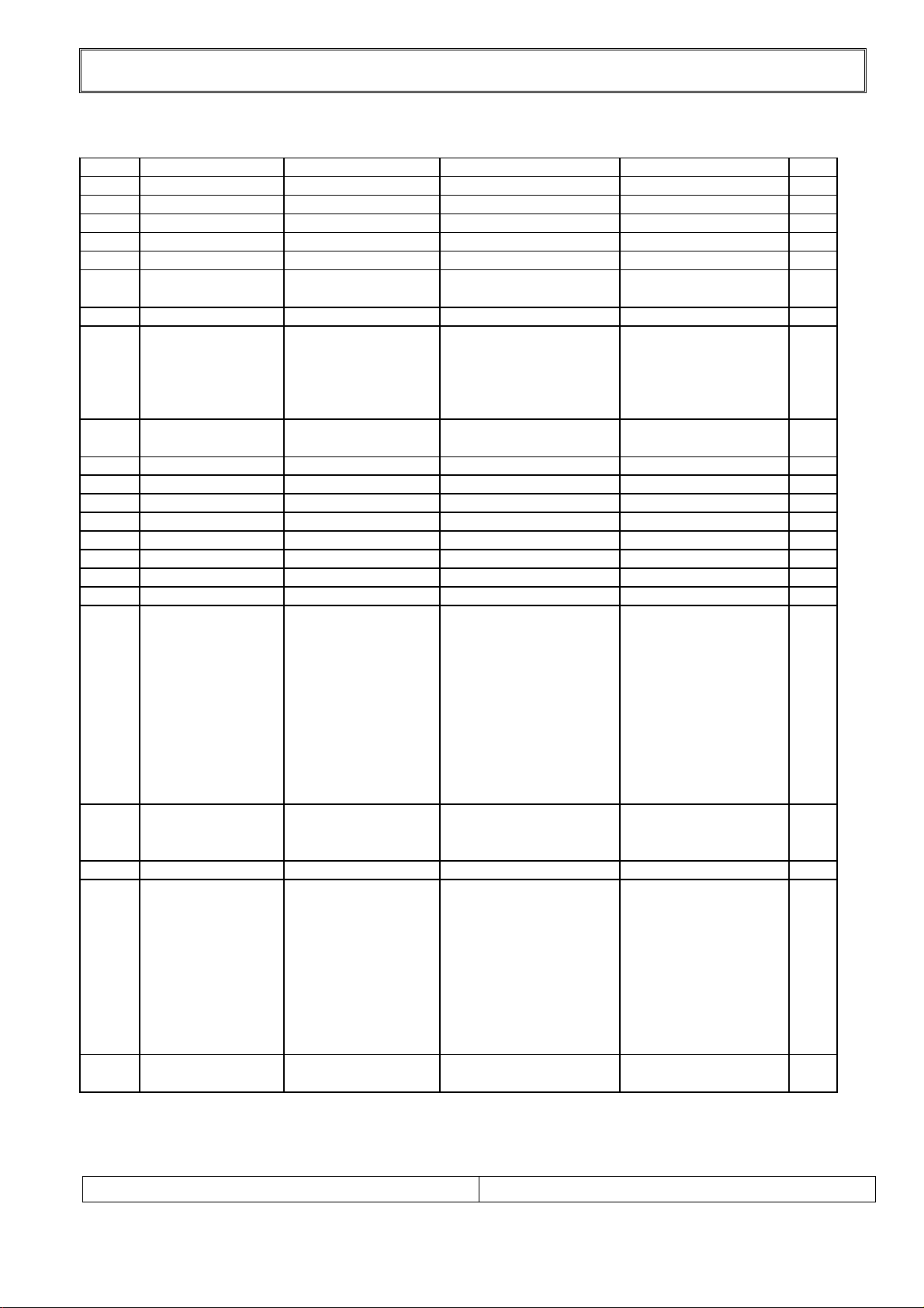
REPLACEMENT PART LIST
C624,C625,C626,C627
L102,L205,L366,L501,L1
6. Parts List (Main PCB)
LEVEL PART NO PART NAME DESCRIPTIONS LOCATION NO Q,TY
0CHSS152DKTS 1500PF,1608 CAPACITOR, CHIP C602,C619,C636 3
2
0CHSS220DJTS 22PF,1608 CAPACITOR, CHIP C235,C236,C503,C504 4
2
0CHSS221DJTS 220PF,1608 CAPACITOR, CHIP C604 1
2
0CHSS224DZTS 0.22UF,1608 CAPACITOR, CHIP C30 1
2
0CHSS330DJTS 33PF,1608 CAPACITOR, CHIP C13,C14 2
2
0CHSS334DZTS 0.33UF,1608 CAPACITOR, CHIP
2
0CHSS470DJTS 47PF,1608 CAPACITOR, CHIP C1009,C1010 2
2
0CHSS471DJTS 470PF,1608 CAPACITOR, CHIP
2
0CHSS473DKTS 0.047UF,1608 CAPACITOR, CHIP
2
0CHSS560DJTS 56PF,1608 CAPACITOR, CHIP C638,C640,C649 3
2
0CHSS822DJTS 8200PF,1608 CAPACITOR,CHIP C360 1
2
0CHSS823DKTS 0.082UF,1608 CAPACITOR,CHIP C361 1
2
0DSSCB340ATS B340A, 3A DIODE, SCHOTTKY CHIP ZD401 1
2
0ICKE7027FTS KIA7027AF, IC, RESET CHIP IC161,IC502,IC06 3
2
0ICKE7042FTS KIA7042AF, IC, RESET CHIP IC602 1
2
0ICKE7805ATS KIA7805AF 5.0V 1A IC, REGULATOR CHIP IC1001,IC832 2
2
0LBSS301FJTS 300 OHM, 3216 BEAD, CHIP L901,L902,L903 3
2
0LBSS601FJTS 600 OHM, 3216 BEAD, CHIP
2
0LHSS100EKTS 10UH, 2012 INDUCTOR, CHIP
2
0LRSL10100BS 33UH, SMD12128.5 INDUCTOR L802,L401 2
2
0RHSS000DJTS 0 OHM, 1608 J RESISTOR, CHIP
2
C628,C629,C630,C631,
C603,C618,C635,C1013,
C1056,C1057,C1058,C1
059,C1033,C1034,C1035
,C1036,C1052,C1053,C1
054,C1055
C212,C213,C214,C218,
C368,C372,C375
L1002,L113,L17,L171,L1
72,L251,L353,L452,L502
,L503,L505,L604,L807,L
1005,L1006,L103,L104,L
105,L106,L107,L108,L10
9,L110,L1151,L1201,L12
1,L201,L202,L203,L204,
L351,L352,L362,L363,L3
64,L365,L421,L422,L451
,L601,L603,L691,L904,L
931,L531
L1001,L1007,L1008,L10
09,L1010,L1011,L1022,L
1023,L602
R434,R401,R73,C1006,
R1007,R1008,R115,R16
2,R163,R204,R205,R361
,R433,R52,R71,R63,R64
,R62,R212,R512,R513,R
902,R910,R1151,R1154,
R1155,R1156,R364,R11
52,R1153,R365,R206,R2
46,C1049,R51
,
9
16
7
45
9
35
0RHSS000EJTS 0 OHM, 2012 J RESISTOR, CHIP
2
SERVICE MANUAL
12,L360,L361,L1019,R12
84
PAGE:
9
Page 85
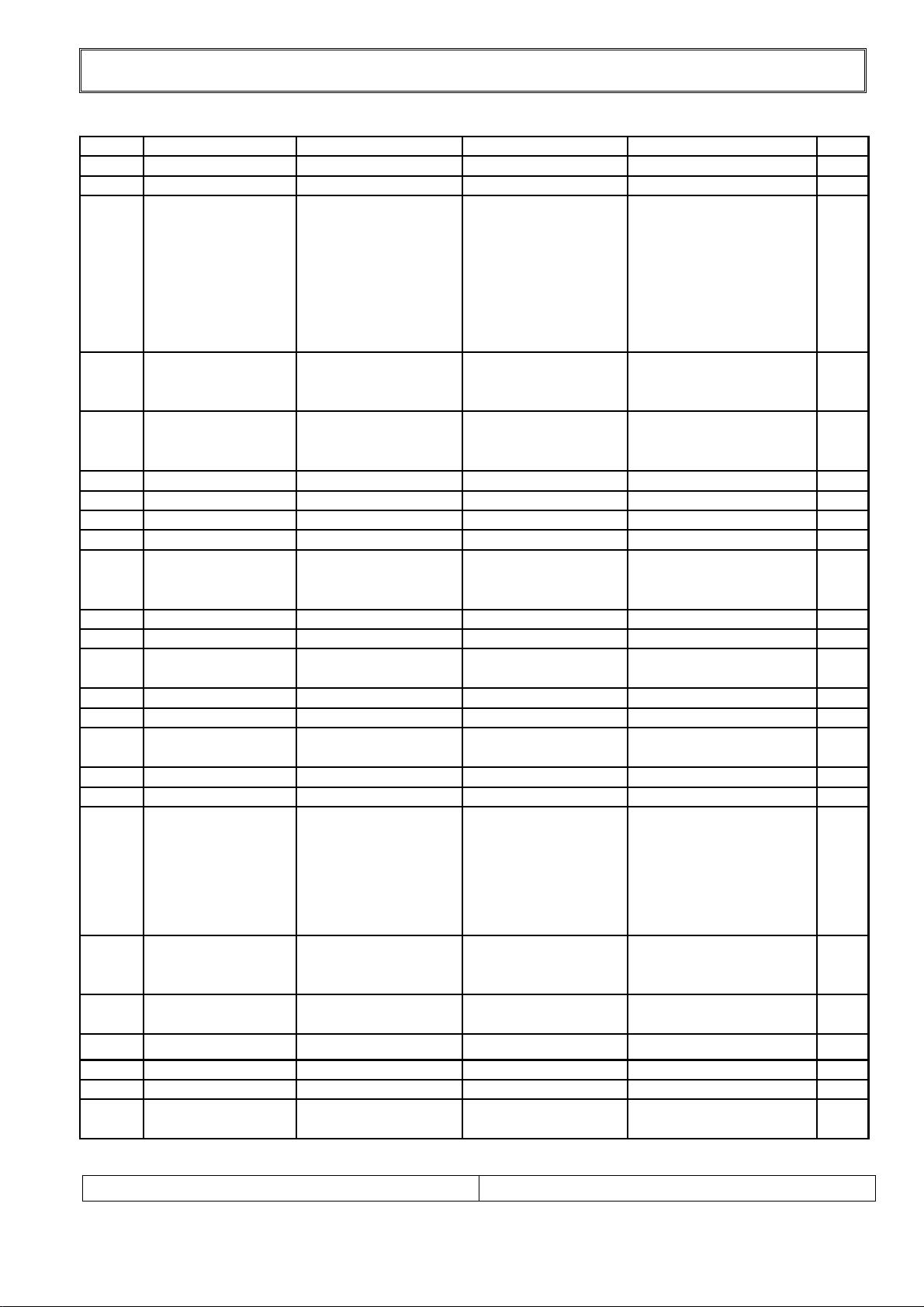
REPLACEMENT PART LIST
7. Parts List (Main PCB)
LEVEL PART NO PART NAME DESCRIPTIONS LOCATION NO Q,TY
2 0RHSS010DJTS 1 OHM, 1608 J RESISTOR, CHIP R1013 1
2 0RHSS100DJTS 10 OHM, 1608 J RESISTOR, CHIP R609,R623 2
R17,R19,R22,R33,R34,R3
5,R37,R39,R40,R41,R42,
R43,R47,R48,R49,R50,R6
2 0RHSS101DJTS 100 OHM, 1608 J RESISTOR, CHIP
2 0RHSS102DJTS 1K OHM, 1608 J RESISTOR, CHIP
2 0RHSS103DJTS 10K OHM, 1608 J RESISTOR, CHIP
2 0RHSS104DJTS 100K OHM, 1608 J RESISTOR, CHIP R1001 1
2 0RHSS105DJTS 1M OHM, 1608 J RESISTOR, CHIP R102 1
2 0RHSS122DJTS 1.2K OHM, 1608 J RESISTOR, CHIP R1002 1
2 0RHSS152DJTS 1.5K OHM, 1608 J RESISTOR, CHIP R637,R639 2
2 0RHSS220DJTS 22 OHM, 1608 J RESISTOR, CHIP
2 0RHSS221DJTS 220 OHM, 1608 J RESISTOR, CHIP R1086 1
2 0RHSS222DJTS 2.2K OHM, 1608 J RESISTOR, CHIP R801 1
2 0RHSS223DJTS 22K OHM, 1608 J RESISTOR, CHIP
2 0RHSS272DJTS 2.7K OHM, 1608 J RESISTOR, CHIP R352 1
2 0RHSS331DJTS 330 OHM, 1608 J RESISTOR, CHIP R1085 1
2 0RHSS332DJTS 3.3K OHM, 1608 J RESISTOR, CHIP
2 0RHSS333DJTS 33K OHM, 1608 J RESISTOR, CHIP R27 1
2 0RHSS392DJTS 3.9K OHM, 1608 J RESISTOR, CHIP R621,R622,R631 3
2 0RHSS470DJTS 47 OHM, 1608 J RESISTOR, CHIP
5,R901,R1014,R1042,R36
,R38,R44,R45,R46,R604,
R605,R608,R640,R641,R2
9,R30,R223,R224
R1009,R1010,R1025,R10
49,R1084,R53,R54,R56,R
55,R606,R607
R161,R453,R454,R455,R5
04,R603,R61,R909,R911,
R924
R103,R104,R105,R211,R2
26,R501,R502,R503,R225
,R908
R1011,R1048,R451,R452,
R1082,R802
R2,R4,R6,R8,R10,R12,R1
4,R16,R18,R20,R21,R67
R110,R112,R114,R1201,R
1202,R1203,R356,R357,R
362,R363,R368,R505,R50
6,R904,R905,R131,R201,
R202,R601,R602,R919,R9
20,L1020,L1021
34
11
10
10
6
12
24
R101,R1161,R1081,R422,
2 0RHSS472DJTS 4.7K OHM, 1608 J RESISTOR, CHIP
2 0RHSS473DJTS 47K OHM, 1608 J RESISTOR, CHIP
2 0RHSS4R7DJTS 4.7 OHM, 1608 J RESISTOR, CHIP R691,R692 2
2 0RHSS510DJTS 51 OHM, 1608 J RESISTOR, CHIP R219,R220,R221 3
2 0RHSS511DJTS 510 OHM, 1608 J RESISTOR, CHIP R351 1
2 0RHSS750DJTS 75 OHM, 1608 J RESISTOR, CHIP
R57,R58,R59,R917,R918,
R931,R932
R1012,R1047,R60,R636,R
638,R1083,R1162,R925
R1017,R1043,R921,R922,
R923
SERVICE MANUAL
PAGE:
85
11
8
5
Page 86
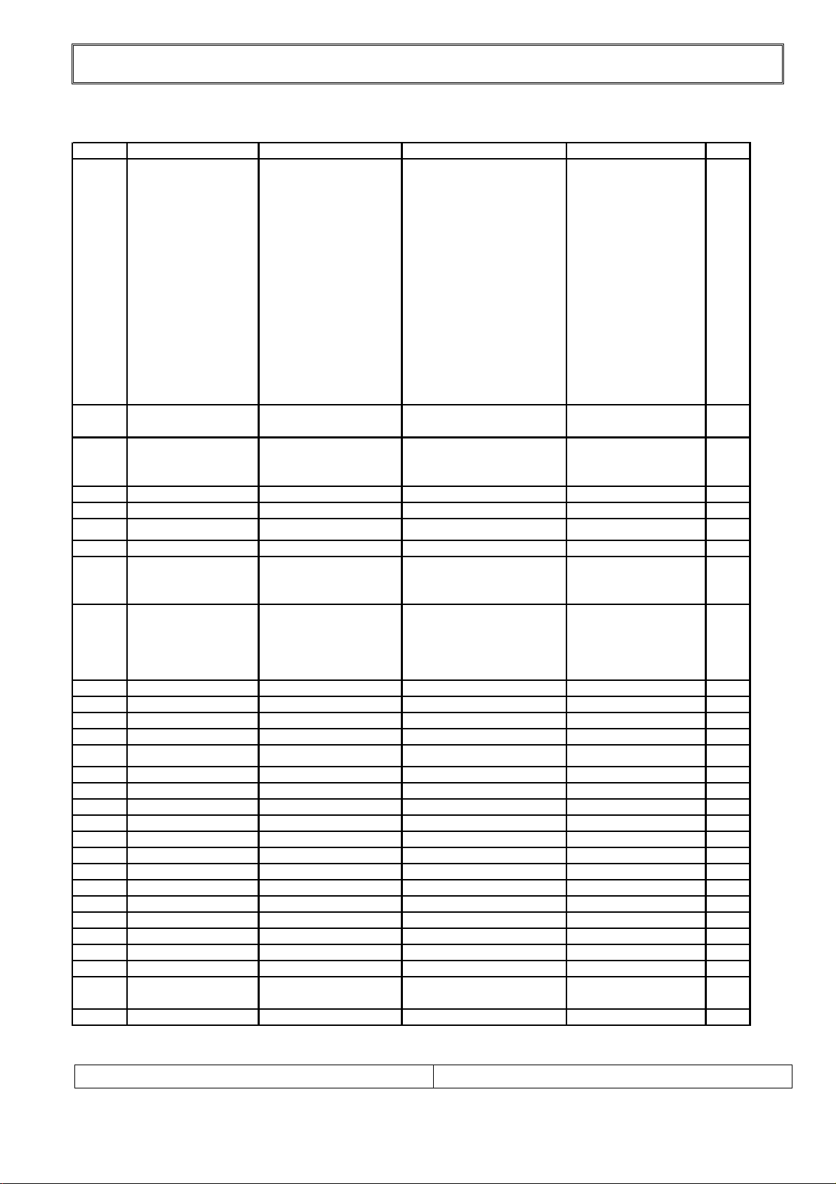
REPLACEMENT PART LIST
0
K
K
K
8. Parts List (Main PCB)
LEVEL PART NO PART NAME DESCRIPTIONS LOCATION NO Q,TY
AL102,AL103,AL104,A
L108,AL109,AL110,AL
114,AL115,AL171,AL1
72,AL173,AL174,AL17
5,AL176,AL177,AL178
,AL179,AL180,AL181,
2 0RYSS330FJTS 33 OHM, 3216 RESISTOR, ARRAY CHIP
AL182,AL183,AL184,A
L185,AL186,AL187,AL
188,AL189,AL190,AL1
91,AL192,AL193,AL19
4,AL195,AL196,AL197
,AL198,AL201,AL202,
AL01,AL02,AL501,AL5
02,AL505
50
2 0TRKE1504STS KTA1504 TRANSISTOR, CHIP
2 0TRKE3875STS KTC3875S TRANSISTOR, CHIP
2 0XTKI06M00TS 6.0MHZ, 33PF CRYSTAL, CHIP X1 1
2 0XTKI143180S 14.318MHZ CRYSTAL, CHIP X101 1
2 0XTKI20M25TS 20.25MHZ, 22PF CRYSTAL, CHIP X201,X501 2
2 1DHSTS1545GS D2PAK, 45V 15A DIODE, RECTIFIER ZD801 1
2 1DHSTYW020TS SMBYW02-200 DIODE, CHIP
2 1DZSC5231BTS 5.1V, MMSZ5231BS-7 DIODE, ZENER CHIP
2 1DZSC5237BTS 8.2V DIODE, ZENER CHIP ZD601 1
2 1ICAD98820BS AD9882A-100MHZ IC, A/D CONVERTER IC351 1
2 1ICIPAP5R0BD AP1501-5.0 IC, DC/DC CONVERTER IC401 1
2 1ICMI5550MBS Txt-pro,PQFP-100 IC, MICOM SDA555OM IC01 1
2 1ICMI9417BCS VSP9417B-C3 IC, VIDEO DECODER IC201 1
2 1ICMI9429AAS FRC9429A-A1(80P) IC, VIDEO DECODER IC501 1
2 1ICMX88L285S MX88L285-S IC, SCALER IC101 1
2 1ICNS90C383S DS90C383S,64MHZ,24 IC, LVDS TRANSMITTER IC402 1
2 1ICNSLM5R0BS 3A, LM2576HVSX-5.0V IC, REGULATOR IC801 1
2 1ICPH74F08TS N74F08, PHLIPS IC, AND GATE IC902 1
2 1ICRO6161FTS ROHM, BA6161F 30~4
2 1ICSE24C16TS 24C16,16K IC, EEPROM IC02 1
2 1ICST24C02WS 24C02W IC, EEPROM IC931,IC901 2
2 1ICST4053BMS HCF4053BM1 IC, TRIPPLE IC1151 1
2 1ICSTLD18DTS LD1085D2M18R,D2PA
2 1ICSTLD25DTS LD1085D2M25R,D2PA
2 1ICSTLD25TTS LD1117S25TR Regulator(STM) IC12 1
2 1ICSTLD33DTS LD1085D2M33R,D2PA
2 1ICSTLD33TTS LD1117S33TR Regulator(STM)
2 1ICWB986532S 512Kx32bitx4 SDRAM IC, SDRAM CHIP IC171,IC172 2
IC, REGULATOR IC1003 1
REGULATOR, IC IC504,IC271 2
IC, REGULATOR IC842 1
IC, REGULATOR IC841 1
Q201,Q202,Q621,Q62
2,Q623,Q203
Q451,Q452,Q1081,Q1
003,Q1009,Q1152,Q3,
Q801,Q921
D831,D832,D834,D83
5,D501
ZD901,ZD902,ZD903,
ZD904,ZD905,ZD1005
,ZD1006,ZD906,ZD90
7,
IC11,IC353,IC503,IC8
51,IC272
6
9
5
9
5
SERVICE MANUAL
PAGE:
86
Page 87
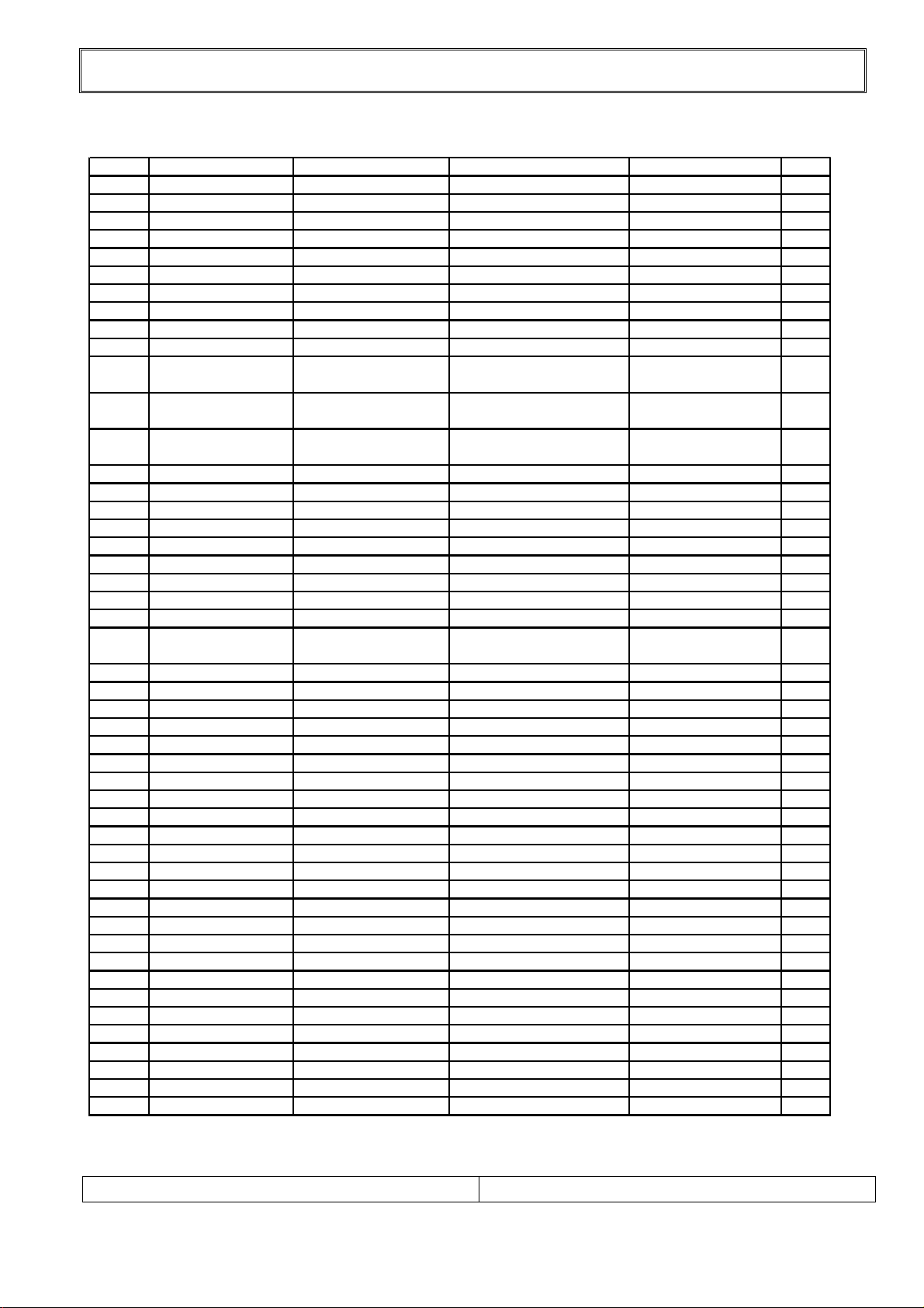
REPLACEMENT PART LIST
T
T
9. Parts List (Main PCB)
LEVEL PART NO PART NAME DESCRIPTIONS LOCATION NO Q,TY
2 WAFYH30125AS 30P, P125, ANGLE WAFER, PIN P451 1
1 GRLT34AS001E TEXT SMD INSERT GR, 40" TEXT S/I 1
2 0RHSS000DJTS 0 OHM, 1608 J RESISTOR, CHIP R24 1
2 0RHSS221DJTS 220 OHM, 1608 J RESISTOR, CHIP R25 1
2 0RHSS392DJTS 3.9K OHM, 1608 J RESISTOR, CHIP R28 1
1 GRLT34AS001G SCART SMD INSERT GR, 40" SCART. S/I 1
2 0CASH220CMTS 22UF 16V CAPACITOR,CAN C1066,C1067 2
2 0CASH2R2HMTS 2.2UF 50V CAPACITOR,CAN C1073 1
2 0CASH471AMTS 470UF 10V CAPACITOR,CAN C1072 1
2 0CHSS104DZTS 0.1UF,1608 CAPACITOR, CHIP C8,C245 2
2 0CHSS471DJTS 470PF,1608 CAPACITOR, CHIP
2 0CHSS473DKTS 0.047UF,1608 CAPACITOR, CHIP
2 0LHSS100EKTS 10UH, 2012 INDUCTOR, CHIP
2 0RHSS000DJTS 0 OHM, 1608 J RESISTOR, CHIP R214 1
2 0RHSS010DJTS 1 OHM, 1608 J RESISTOR, CHIP R1052 1
2 0RHSS102DJTS 1K OHM, 1608 J RESISTOR, CHIP R1050,R1051,R1054 3
2 0RHSS153DJTS 15K OHM, 1608 J RESISTOR, CHIP R31 1
2 0RHSS223DJTS 22K OHM, 1608 J RESISTOR, CHIP R1055 1
2 0RHSS331DJTS 330 OHM, 1608 J RESISTOR, CHIP R231,R232,R233 3
2 0RHSS471DJTS 470 OHM, 1608 J RESISTOR, CHIP R241 1
2 0RHSS472DJTS 4.7K OHM, 1608 J RESISTOR, CHIP R242 1
2 0RHSS473DJTS 47K OHM, 1608 J RESISTOR, CHIP R32,R1056 2
2 0RHSS750DJTS 75 OHM, 1608 J RESISTOR, CHIP
2 0TRKE3875STS KTC3875S TRANSISTOR, CHIP Q241,Q1051 2
1 GRLT34AS001H SOUND 1 SMD INSER
2 0CASH101EMTS 100UF 25V CAPACITOR,CAN C654 1
2 0CASH2R2HMTS 2.2UF 50V CAPACITOR,CAN C652,C656 2
2 0CASH330CMTS 33UF 16V CAPACITOR,CAN C675 1
2 0CHSS103DKTS 0.01UF,1608 CAPACITOR, CHIP C661 1
2 0CHSS332DKTS 3300PF,1608 CAPACITOR, CHIP C653,C655 2
2 0RHSS101DJTS 100 OHM, 1608 J RESISTOR, CHIP R658,R681,R682 3
2 0RHSS2R2DJTS 2.2 OHM, 1608 J RESISTOR, CHIP R657,R663 2
2 0RHSS472DJTS 4.7K OHM, 1608 J RESISTOR, CHIP R653,R654 2
2 0RHSS473DJTS 47K OHM, 1608 J RESISTOR, CHIP R659,R660 2
2 0RHSS561DJTS 560 OHM, 1608 J RESISTOR, CHIP R651,R656 2
2 0TRKE3875STS KTC3875S TRANSISTOR, CHIP Q651 1
1 GRLT34AS001J SOUND 2 SMD INSER
2 0CASH101EMTS 100UF 25V CAPACITOR,CAN C668 1
2 0CASH2R2HMTS 2.2UF 50V CAPACITOR,CAN C666,C670 2
2 0CASH330CMTS 33UF 16V CAPACITOR,CAN C679 1
2 0CHSS103DKTS 0.01UF,1608 CAPACITOR, CHIP C674 1
2 0CHSS332DKTS 3300PF,1608 CAPACITOR, CHIP C667,C669 2
2 0RHSS101DJTS 100 OHM, 1608 J RESISTOR, CHIP R665,R668,R672 3
2 0RHSS2R2DJTS 2.2 OHM, 1608 J RESISTOR, CHIP R670,R676 2
2 0RHSS472DJTS 4.7K OHM, 1608 J RESISTOR, CHIP R666,R667 2
2 0RHSS473DJTS 47K OHM, 1608 J RESISTOR, CHIP R671,R673 2
2 0RHSS561DJTS 560 OHM, 1608 J RESISTOR, CHIP R664,R669 2
2 0TRKE3875STS KTC3875S TRANSISTOR, CHIP Q652 1
GR, 40" SOUND 1 S/I 1
GR, 40" SOUND 2 S/I 1
C1064,C1065,C1068,
C1069,C1024,C1025
C239,C240,C241,C24
2,C243,C244
L1013,L1015,L1062,L
1063,L1064,L1065
R1019,R1020,R1021,
R1053
6
6
6
4
SERVICE MANUAL
PAGE:
87
Page 88
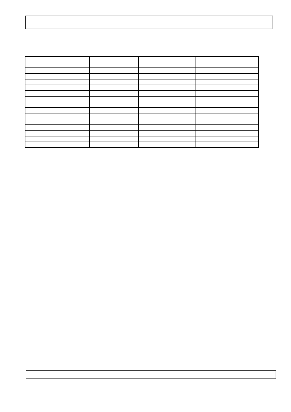
REPLACEMENT PART LIST
10. Parts List (Main PCB )
LEVEL PART NO PART NAME DESCRIPTIONS LOCATION NO Q,TY
1 GRLT34AS001M TUNER SMD INSERT GR,40"TUNER.SECAM S/ 1
2 0CASH100CMTS 10UF 16V CAPACITOR,CAN C26 1
2 0CASH221AMTS 220UF 10V CAPACITOR,CAN C1060 1
2 0CASH4R7HMTS 4.7UF 50V CAPACITOR,CAN C1015 1
2 0CHSS104DZTS 0.1UF,1608 CAPACITOR, CHIP C25 1
2 0CHSS334DZTS 0.33UF,1608 CAPACITOR, CHIP C1016 1
2 0ICHNV8100BS 128K x 8bit, 70ns IC, SDRAM CHIP IC04 1
2 0LBSS601FJTS 600 OHM, 3216 BEAD, CHIP L16 1
2 0RHSS000DJTS 0 OHM, 1608 J RESISTOR, CHIP R74 1
2 0RHSS103DJTS 10K OHM, 1608 J RESISTOR, CHIP
2 0RHSS221DJTS 220 OHM, 1608 J RESISTOR, CHIP R1004,R1003 2
2 0TRKE102S0TS KRC102S TRANSISTOR, CHIP Q1002 1
2 0TRKE3875STS KTC3875S TRANSISTOR, CHIP Q1001,Q1007 2
2 1ICMI3410DBS MSP3410D/G, SMD IC, SOUND DECODER IC601 1
R1005,R1006,R1061,
R1026
4
SERVICE MANUAL
PAGE:
88
Page 89
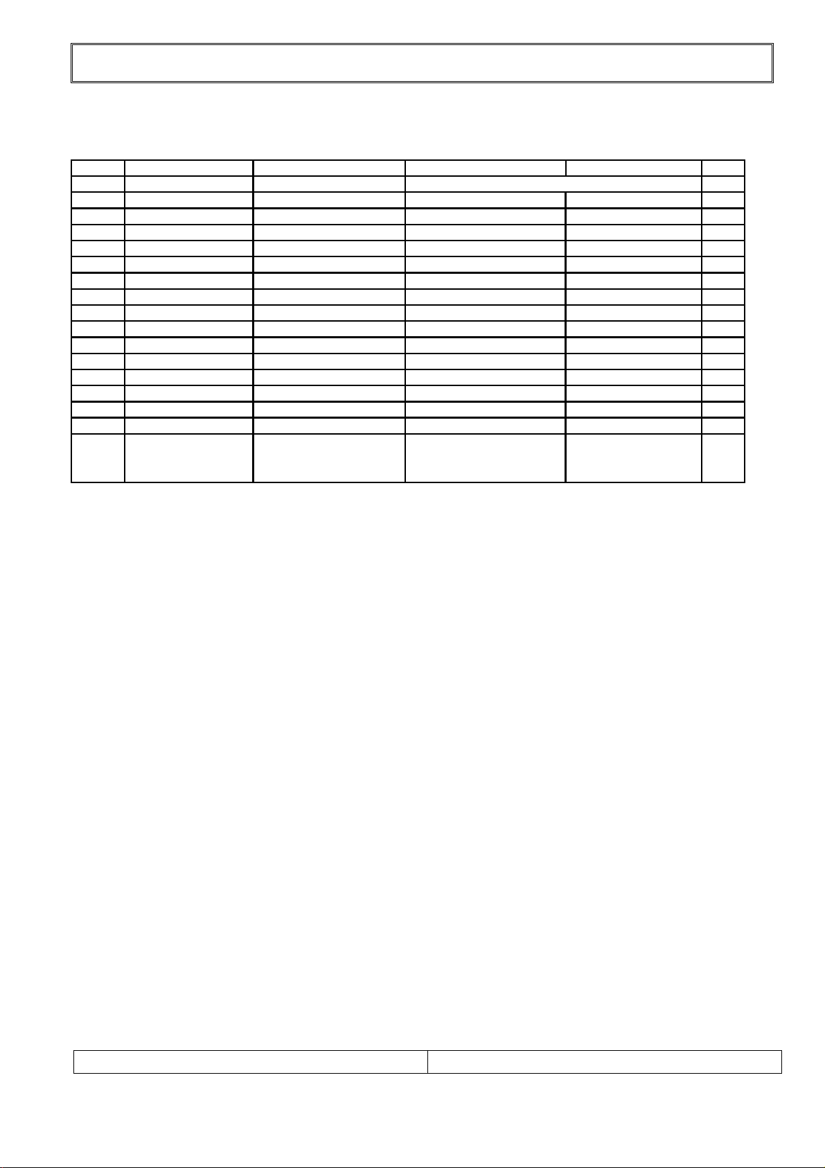
REPLACEMENT PART LIST
11. Parts List (Control PCB )
LEVEL PART NO PART NAME DESCRIPTIONS LOCATION NO Q,TY
1 AYCOLT32A01B CONTROL PCB ASS'Y F/N MODEL, 111-A34A-30 CONTROL 1
2 GRLT32AS002A GR, 30" Control S/I CTRL,SMD INSERT 1
3 111-A34B PCB, CONTROL H/M MODEL CONTROL 1
3 0TRKE3875STS TRANSISTOR, CHIP KTC3875S Q3001,Q3002,Q3004 3
3 0RHSS472DJTS RESISTOR, CHIP 4.7K OHM, 1608 J R3012,R3014,R3016 3
3 0RHSS471DJTS RESISTOR, CHIP 470 OHM, 1608 J R3011,R3013 2
3 0RHSS222DJTS RESISTOR, CHIP 2.2K OHM, 1608 J R3002,R3003,R3005 3
3 0RHSS120DJTS RESISTOR, CHIP 12 OHM, 1608 J R3015 1
3 0RHSS102DJTS RESISTOR, CHIP 1K OHM, 1608 J R3001,R3004 2
3 0CHSS101DJTS CAPACITOR, CHIP 100PF,1608 C3001 1
2 GRLT32AM002A GR, 30" Control M/I CTRL,MANUAL INSERT 1
3 WAFYH10200AD WAFER, PIN 10-PIN, P2.0mm ANGLE P108 1
3 WAFYH05200AD WAFER, PIN 5-PIN, P2.0mm ANGLE P11A,P11B 2
3 0PAVI48380AD PRE-AMP PRE-AMP, 38KHZ PA3001 1
3 0DLSYRG138AD DIODE, LED RED, SL RG138 BIG SIZE LD3001 1
2 GRLT32AA002A GR, 30" Control A/I CTRL,AUTO INSERT 1
SW3001,SW3002,SW
3 600-002A SWITCH, TACT YTP-1141A
3003,SW3004,SW300
5,SW3006,SW 3007
7
SERVICE MANUAL
PAGE:
89
Page 90

1. Block Diagram
BLOCK DIAGRAM
SERVICE MANUAL
PAGE:
90
Page 91
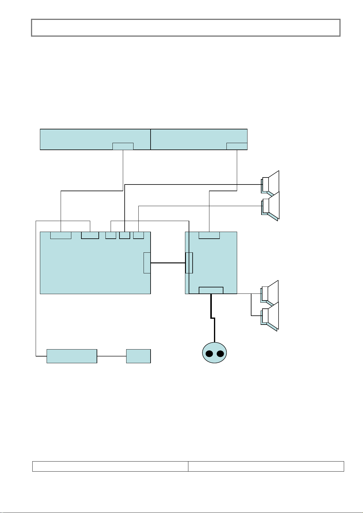
1. Connection diagram
PANEL INVERTER
CONNECTION DIAGRAM
30PIN
MAIN Board
4PIN
2PIN
3PIN
14PIN
14PIN
SMPS
Board
3 PIN
L
R
MAIN
SPEAKER
10 PIN
5 PIN
CONTROL IR
SERVICE MANUAL
Power Cord
SUB
SPEAKER
91
PAGE:
Page 92

1.Schematic Diagram
SCHEMATIC DIAGRAM
SERVICE MANUAL
PAGE:
92
Page 93
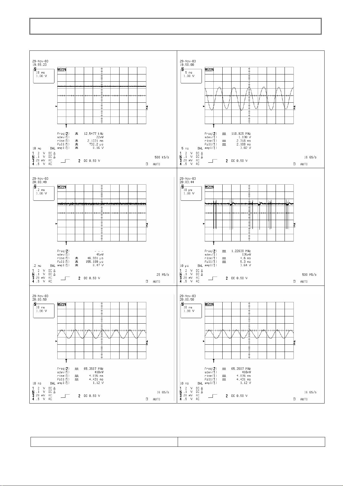
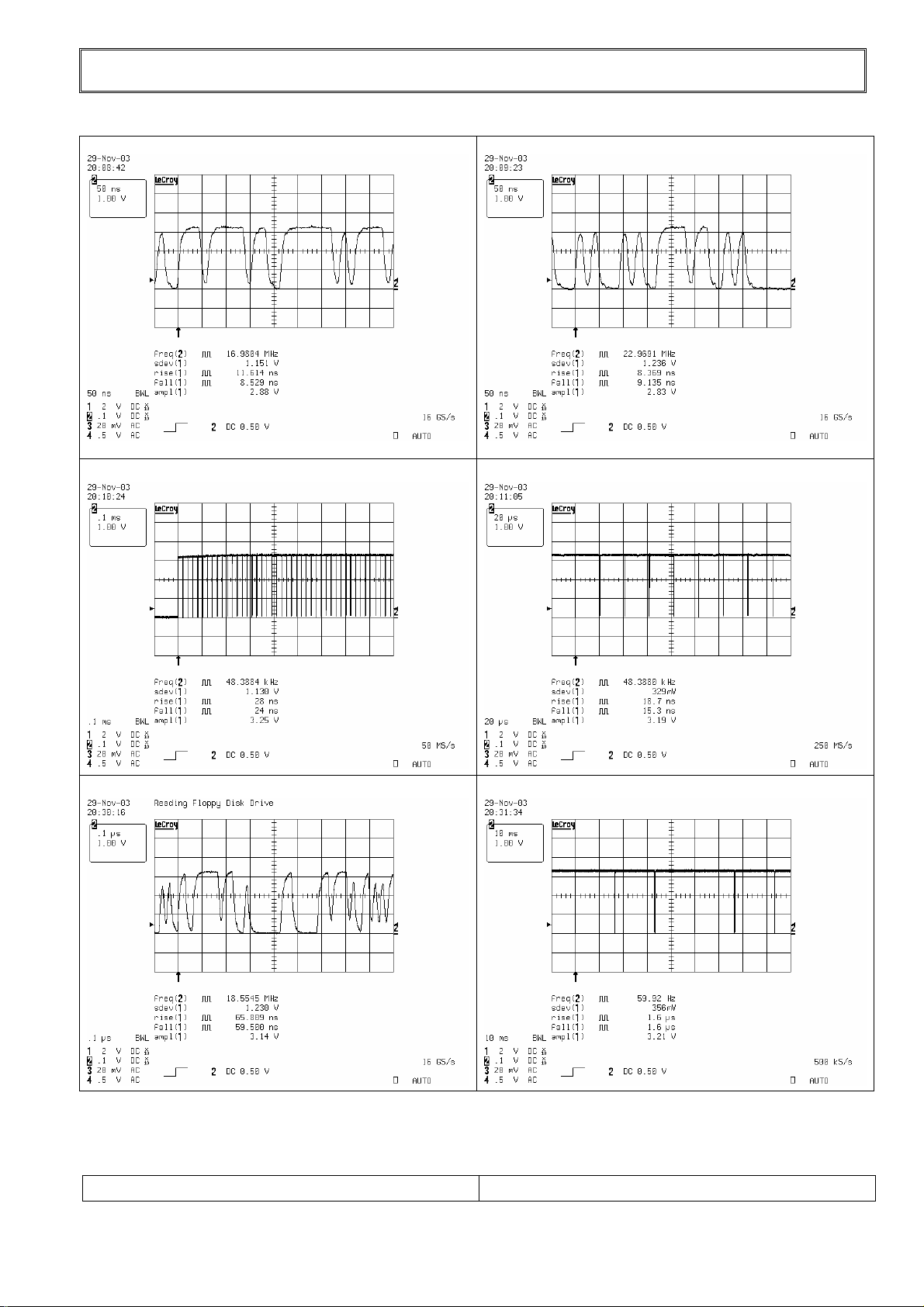
WAVE FORM
NOTE!!: You can find number from Schematic Diagram
1)IC101 PIN27 - MCKA 2)IC801 PIN26 - MCLK
3)IC101 PIN 24 - MCKE 4) )IC101 PIN 23 - MCAS
5) IC101 PIN 380 - LCLKA 6) ) IC101 PIN 378 - LCLKA
SERVICE MANUAL
PAGE:
93
Page 94
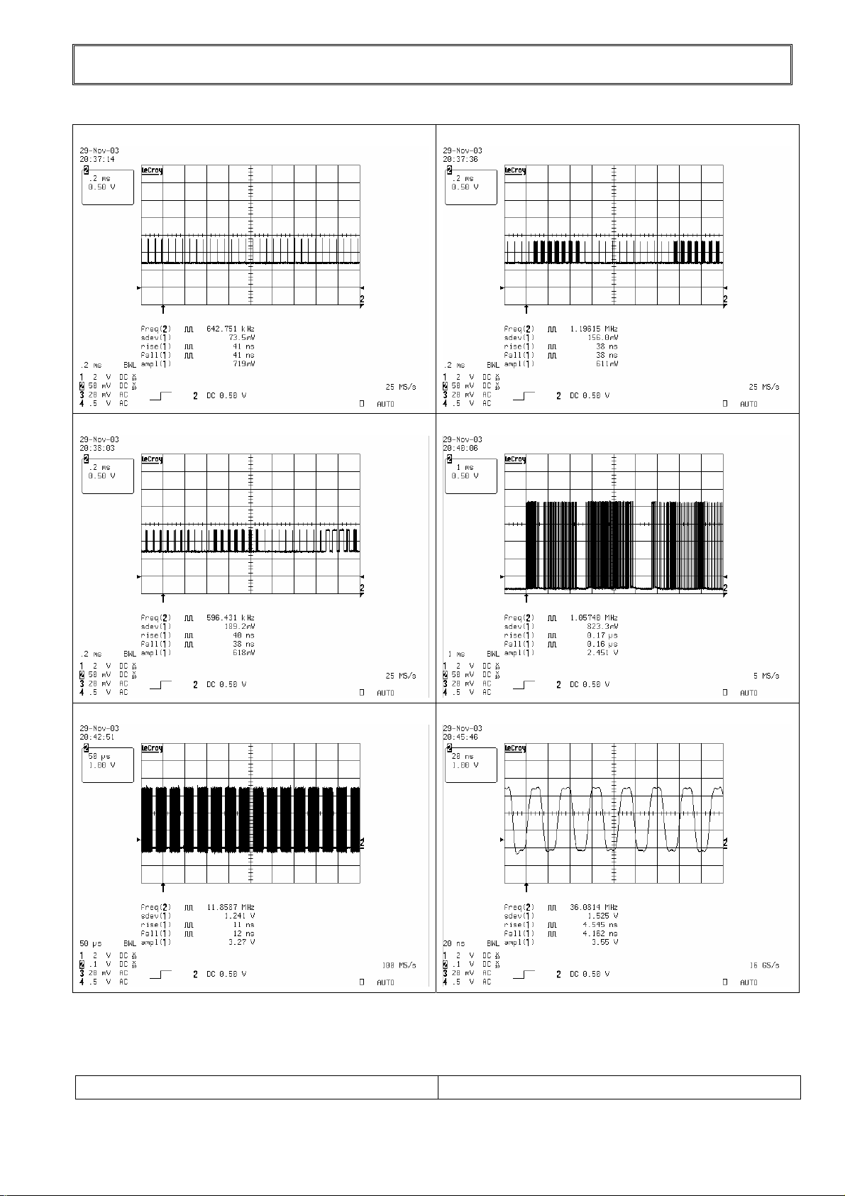
WAVE FORM
NOTE!!: You can find number from Schematic Diagram
7) IC101 PIN 369 – B signal OUT
8) IC101 PIN 346 – G signal OUT
9) IC101 PIN 327 - LDTG 10)IC101 PIN 326 H- sync
11) IC101 PIN 328 R signal out 12)IC 101 pin 301 V-sync
SERVICE MANUAL
PAGE:
94
Page 95
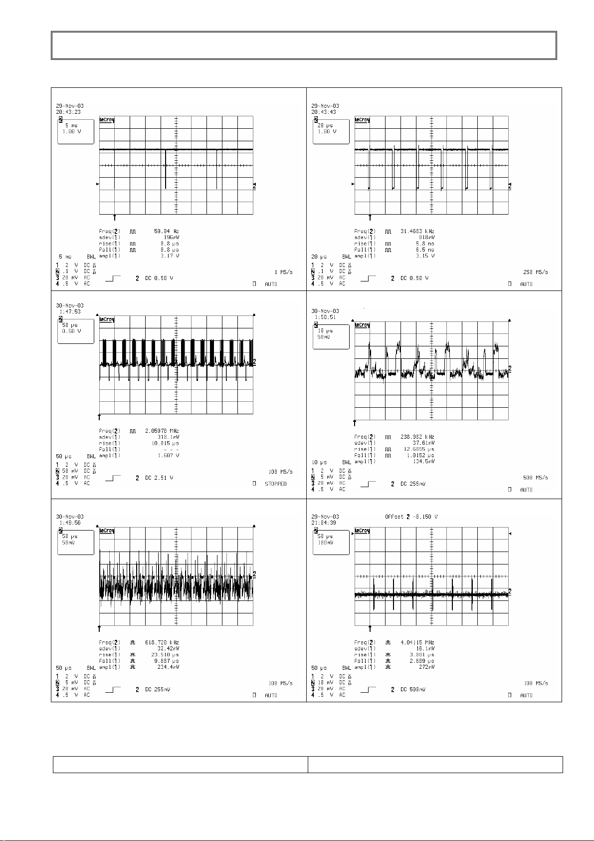
WAVE FORM
NOTE!!: You can find number from Schematic Diagram
13) IC 201 pin 40 TELETEXT B signal input 14) IC 201 pin 39 TELETEXT G signal input
15) IC 201 pin 38 TELETEXT R signal.input 16) IC 201 pin 37 TELETEXT FB signal input
17) IC201 pin 54 R signal output 18) IC 201 pin 51 clock output
SERVICE MANUAL
PAGE:
95
Page 96
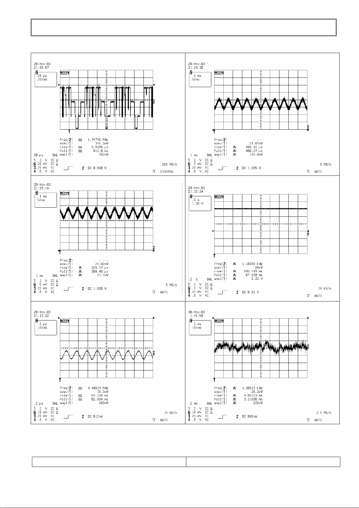
WAVE FORM
NOTE!!: You can find number from Schematic Diagram
19) IC201 pin 23 V-output 20) IC201 pin 17 H-output
21) IC201 pin 80 Component Y - signal input
23) IC201 pin 82 Component U - signal input 24) IC201 pin 55 S-Video C signal input
22) IC201 pin 78 Component V - signal input
SERVICE MANUAL
PAGE:
96
Page 97
WAVE FORM
NOTE!!: You can find number from Schematic Diagram
25) IC201 PIN 56 S-Video Y signal input 26) IC691 pin 3 HEAD_PHONE L -sound output
27) IC691 pin 1 HEAD_PHONE R -sound output
29) IC601 pin 67 SIF signal input 30) IC601 pin 56&57 AV1 sound input(video)
28) IC651& 652 pin 8 MUTE
SERVICE MANUAL
PAGE:
97
Page 98
WAVE FORM
NOTE!!: You can find number from Schematic Diagram
31) IC601 pin 50&51 sound input(phone -2P)
33) IC601 pin 28 L -sound output 34) IC601 pin 27 R- sound output
32) IC601 pin 47&48 sound input ( PC )
( XGA 1024*768@60HZ )
35) IC351 pin 99 R signal ouput
( XGA 1024*768@60HZ)
SERVICE MANUAL
36) IC351 pin 10 G signal ouput
( XGA 1024*768@60HZ)
PAGE:
98
Page 99
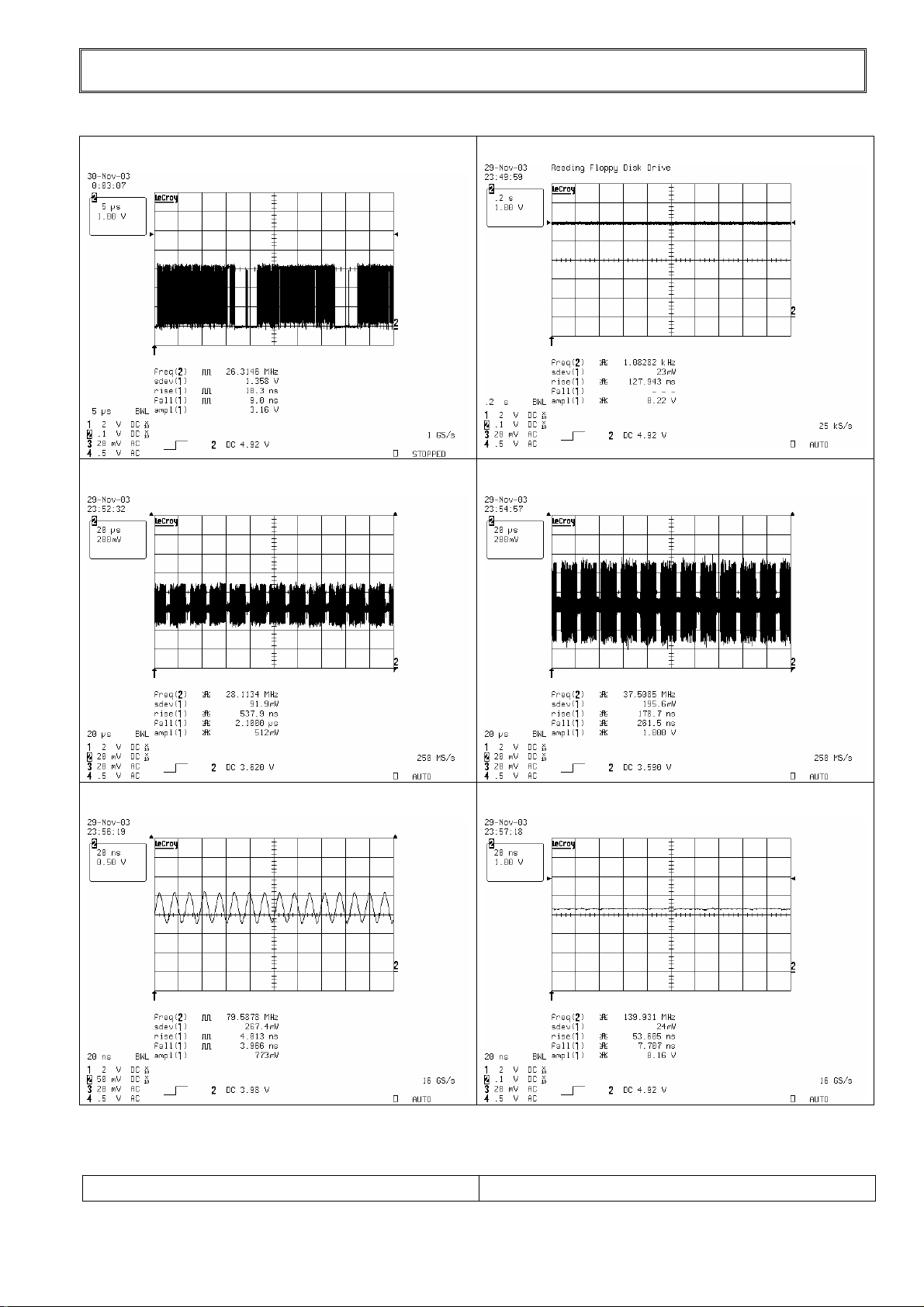
WAVE FORM
NOTE!!: You can find number from Schematic Diagram
37) IC351 pin 20 B signal ouput
( XGA 1024*768@60HZ)
38) IC301 5V (VCC)
39) IC351 RX0+ signal
( XGA 1024*768@60HZ )
41) IC351 pin 85 data clock
( XGA 1024*768@60HZ)
40) IC351 RX2+ signal
( XGA 1024*768@60HZ ).
42) IC351 pin 86 Disenable
( XGA 1024*768@60HZ)
SERVICE MANUAL
PAGE:
99
Page 100
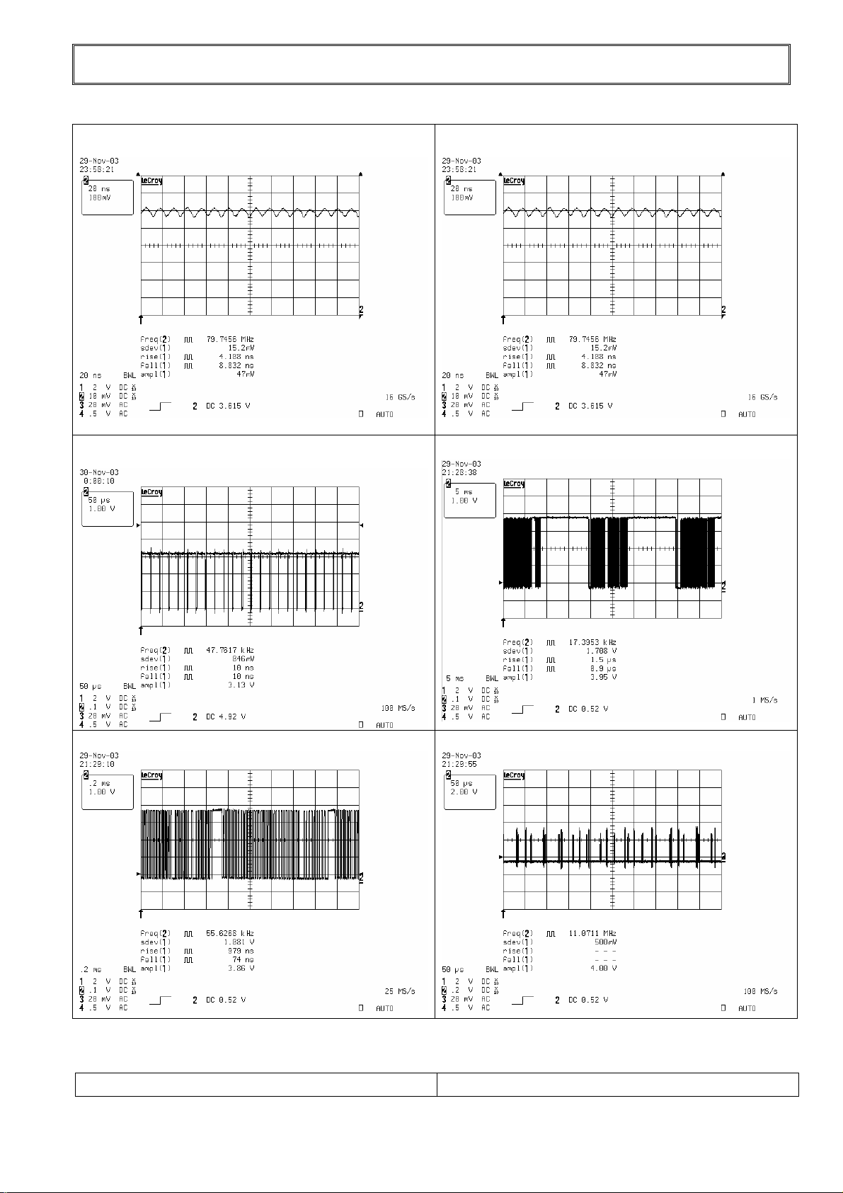
WAVE FORM
NOTE!!: You can find number from Schematic Diagram
43) IC351 pin 87 V - sync output
( XGA 1024*768@60HZ)
44) IC351 pin 88 H - sync output
( XGA 1024*768@60HZ)
45) IC351 pin 89 SOG sync output
( XGA 1024*768@60HZ)
47) IC01 pin 11 SCL clock output 48) IC171 pin 2 data input.
46) IC01 pin 11 SDA clock output
SERVICE MANUAL
PAGE:
100
 Loading...