

Page 1
LT3595
1
3595f
, LT, LTC and LTM are registered trademarks of Linear Technology Corporation.
True Color PWM is a trademark of Linear Technology Corporation. All other trademarks are
the property of their respective owners.
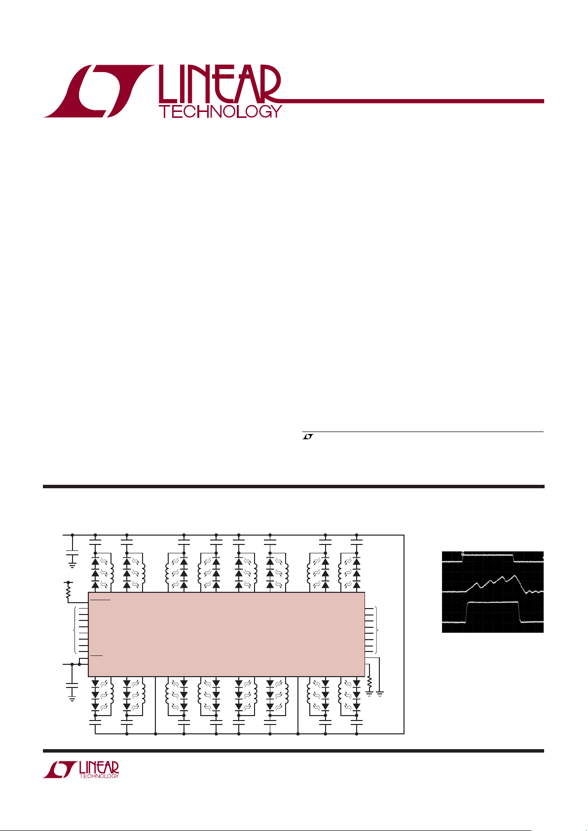
TYPICAL APPLICATION
FEATURES
APPLICATIONS
DESCRIPTION
16 Channel
Buck Mode LED Driver
The LT®3595 is a high performance LED Driver designed
to drive sixteen independent channels of up to 10 LEDs
at currents up to 50mA. Series connection of the LEDs
provides identical LED currents resulting in uniform brightness. Power switches, Schottky diodes, and compensation
components are all internal, providing a small converter
footprint and lower component cost. The high 2MHz
switching frequency permits the use of tiny, low profi le
inductors and capacitors. A fi xed frequency, current mode
architecture results in stable operation over a wide range
of supply and output voltage.
A single external resistor sets the LED current for all sixteen
channels, and dimming is then controlled for each channel
by pulse width modulating the individual PWM pins. Relative current matching among the sixteen drivers is 8% and
the PWM dimming range is 5000:1. The part is available
in a 5mm × 9mm × 0.75mm 56-pin QFN package.
16-Channel LED Driver (Three LEDs per Channel), 20mA Current
■
4.5V to 45V Input Supply Range
■
Up to 50mA LED Current per Channel
■
100mA, 45V Internal Switches
■
8% Relative LED Current Match at 20mA
■
16 Independent LED Channels
■
5000:1 True Color PWMTM Dimming Range
■
LEDs Disconnected in Shutdown
■
Internal Schottky Diodes
■
Low Quiescent Current
■
2MHz Switching Frequency
■
R
SET
Pin Sets Master LED Current
■
Typical Effi ciency: 92%
■
Open LED Detection and Thermal Protection
■
56-Pin 5mm × 9mm × 0.75mm QFN Package
■
LED Video Billboards
■
LCD Televisions
■
Stadium and Advertising Displays
5000:1 PWM
Dimming at 100Hz
V
IN
15V TO
45V
LED
BRIGHTNESS
CONTROL
V
CC
3V TO
5.5V
V
CC
0.47μF 0.47μF 0.47μF 0.47μF 0.47μF 0.47μF 0.47μF 0.47μF
0.47
μF
10
μF
10
μF
100k
75.0k
0.47μF 0.47μF 0.47μF 0.47μF 0.47μF 0.47μF 0.47μF
3595 TA01
OPENLED
PWM1
PWM2
PWM3
PWM4
PWM5
PWM6
PWM7
PWM8
V
CC
PWM9
PWM10
PWM11
PWM12
PWM13
PWM14
PWM15
PWM16
GND
R
SET
L1 SW1 SW2 L4SW3 SW7L3 SW4 L5 L6SW5 SW6L2 L7 SW8 L8
L16 SW16 SW15 V
IN
L13SW14 VINSW10L14 SW13 L12 L11SW12 SW11L15 L10 SW9 L9
100μH
100
μH
100
μH
100μH100
μH
100μH
100
μH
100μH
100
μH
100
μH
100
μH
100μH100
μH
100μH
100
μH
100μH
SHDN
LT3595
LED
BRIGHTNESS
CONTROL
400ns/DIV
I
LED
10mA/DIV
I
SW
20mA/DIV
V
PWM
5V/DIV
3595 TA01
b
V
IN
= 15V
3 LEDS AT 20mA
T = 10ms
T
ON
= 2μs
Page 2
LT3595
2
3595f
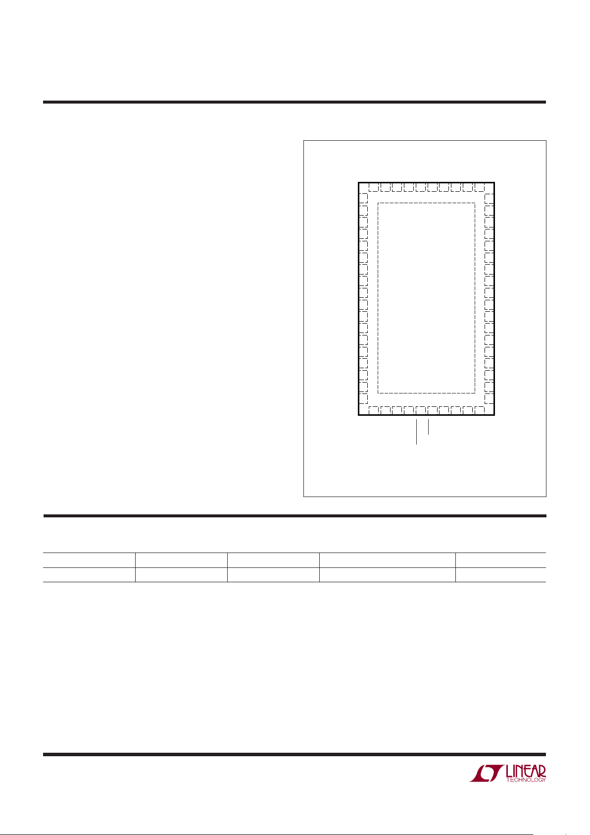
PIN CONFIGURATIONABSOLUTE MAXIMUM RATINGS
Input Voltage (VIN) ....................................................45V
L1-16 Voltage ...........................................................45V
Supply Voltage (V
CC
) ..................................................6V
R
SET
, ⎯O⎯P⎯E⎯N⎯L⎯E⎯D , PWM1-16, ⎯S⎯H⎯D⎯N Voltage ...............6V
Operating Junction Temperature Range
(Note 2) ...............................................–40°C to 85°C
Maximum Junction Temperature .......................... 125°C
Storage Temperature Range ...................–65°C to 125°C
(Note 1)
19 20 21 22
TOP VIEW
57
UHH PACKAGE
56-LEAD (5mm × 9mm) PLASTIC QFN
23 24 25 26 27 28
56 55 54 53 52 51 50 49 48 47
39
40
41
42
43
44
45
46
8
7
6
5
4
3
2
1L16
SW16
L15
SW15
V
IN
SW14
L14
SW13
L13
L12
SW12
L11
SW11
V
IN
SW10
L10
SW9
L9
L1
SW1
L2
SW2
NC
SW3
L3
SW4
L4
L5
SW5
L6
SW6
NC
SW7
L7
SW8
L8
PWM16
PWM15
PWM14
PWM13
VCCR
SET
PWM4
PWM3
PWM2
PWM1
38
37
36
35
34
33
32
31
30
29
9
10
11
12
13
14
15
16
17
18
PWM9
PWM10
PWM11
PWM12
OPENLED
SHDN
PWM5
PWM6
PWM7
PWM8
T
JMAX
= 125°C, θJA = 31°C/W, θJC = 0.5°C/W
EXPOSED PAD (PIN 57) IS GND, MUST BE SOLDERED TO PCB
ORDER INFORMATION
LEAD FREE FINISH TAPE AND REEL PART MARKING PACKAGE DESCRIPTION TEMPERATURE RANGE
LT3595EUHH#PBF LT3595EUHH#TRPBF 3595 56-Lead (5mm × 9mm) Plastic QFN –40°C to 85°C
Consult LTC Marketing for parts specifi ed with wider operating temperature ranges.
Consult LTC Marketing for information on non-standard lead based fi nish parts.
For more information on lead free part marking, go to: http://www.linear.com/leadfree/
For more information on tape and reel specifi cations, go to: http://www.linear.com/tapeandreel/
Page 3
LT3595
3
3595f
ELECTRICAL CHARACTERISTICS
Note 1: Stresses beyond those listed under Absolute Maximum Ratings
may cause permanent damage to the device. Exposure to any Absolute
Maximum Rating condition for extended periods may affect device
reliability and lifetime.
PARAMETER CONDITIONS MIN TYP MAX UNITS
V
IN
Operating Voltage
4.5 V
V
CC
Operating Voltage
3 5.5 V
V
CC
Input Under Voltage Lockout
2.6 2.9 V
I
VIN
Quiescent Current ON, No Switching VIN = 45V 0.25 mA
I
VIN
Quiescent Current in Shutdown VIN = 45V, ⎯S⎯H⎯D⎯N = 0V 15 40 μA
I
VCC
Quiescent Current ON, No Switching VCC = 3.3V 17 mA
I
VCC
Quiescent Current in Shutdown VCC = 3.3V, ⎯S⎯H⎯D⎯N = 0V 3 10 μA
I
L1-16
Output Current Accuracy R
SET
= 75.0kΩ 18.4 20 21.6 mA
Switching Frequency 1.622.4MHz
Maximum Duty Cycle
●
78 83 %
Switch Current Limit
●
90 120 150 mA
Switch V
CESAT
ISW1-16 = 50mA 450 mV
Switch Leakage Current VSW1-16 = 45V 0.1 6 μA
Schottky Forward Drop I
SCHOTTKY
= 50mA 0.8 V
Schottky Leakage Current V
IN
= 45V, V
SW1-16
= 0.7V, ⎯S⎯H⎯D⎯N = 0V 0.1 4 μA
⎯S⎯H⎯D⎯
N, PWM1-16 Input Low Voltage 0.4 V
⎯S⎯H⎯D⎯
N, PWM1-16 Input High Voltage 1.6 V
⎯S⎯H⎯D⎯
N Pin Bias Current
⎯S⎯H⎯D⎯
N = 3.3V 35 μA
PWM1-16 Pin Bias Current PWM1-16 = 3.3V 0.1 1 μA
⎯O⎯P⎯E⎯N⎯L⎯E⎯
D Pin Voltage VCC = 3.3V, I
⎯O⎯P⎯E⎯N⎯L⎯E⎯
D
= 200μA 0.12 V
⎯O⎯P⎯E⎯N⎯L⎯E⎯
D Pin Input Leakage Current
⎯O⎯P⎯E⎯N⎯L⎯E⎯
D = 3.3V 0.1 1 μA
The ● denotes the specifi cations which apply over the full operating
temperature range, otherwise specifi cations are at T
A
= 25°C, VIN = 45V, VCC = 3.3V, PWM = ⎯S⎯H⎯D⎯N = ⎯O⎯P⎯E⎯N⎯L⎯E⎯D = 3.3V, R
SET
= 75kΩ,
GND = 0V, unless otherwise noted.
Note 2: The LT3595 is guaranteed to meet performance specifi cations
from 0°C to 85°C junction temperature. Specifi cations over the – 40°C
to 85°C operating junction temperature range are assured by design,
characterization and correlation with statistical process controls.
Page 4
LT3595
4
3595f
R
SET
RESISTANCE (kΩ)
25
LED CURRENT (mA)
30
50
40
60
50 150
20
10
0
75 100 125
3595 G05
DUTY CYCLE (%)
0.01
LED CURRENT (mA)
1
10
100
0.1
0.01
0.001
0.1
1
10
100
3595 G04
VIN = 45V
10 LEDS AT 20mA
PWM FREQUENCY = 100Hz
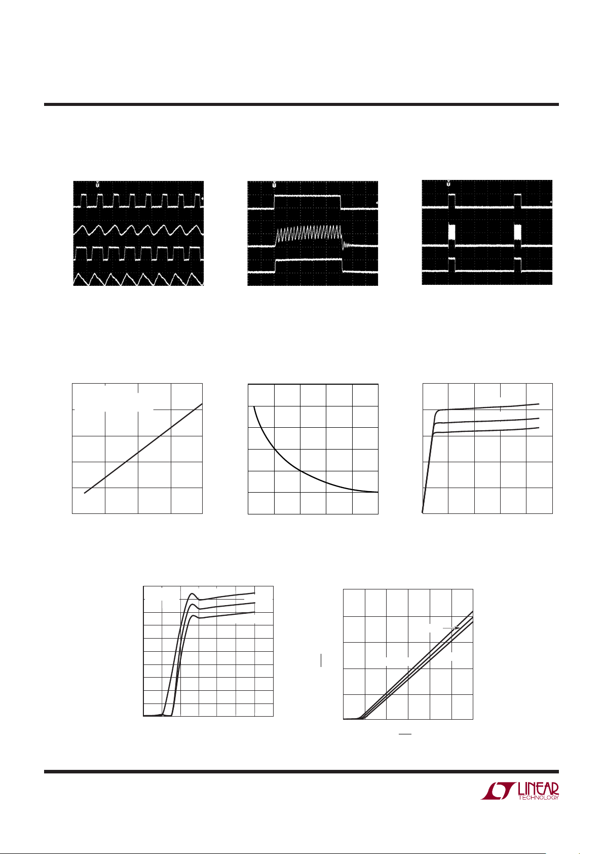
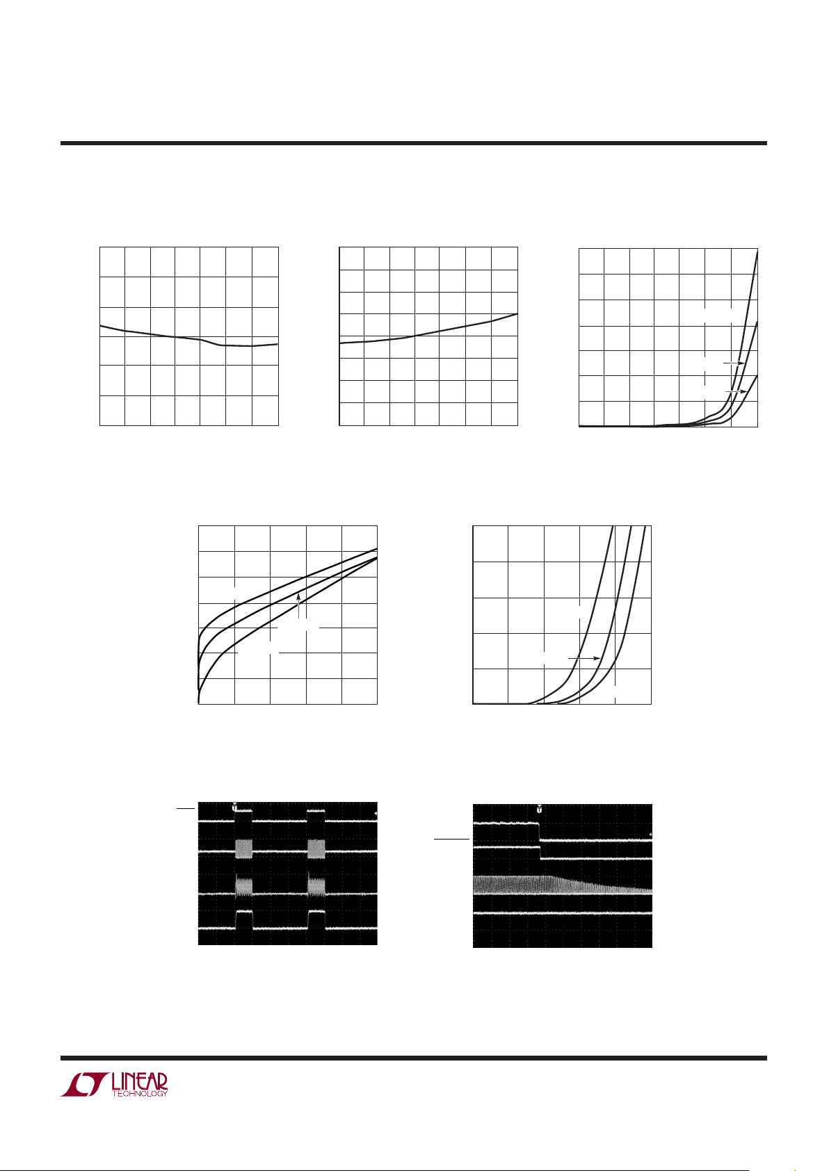
TYPICAL PERFORMANCE CHARACTERISTICS
Switching Waveforms
PWM Dimming Waveforms
(1000:1)
LED Current vs PWM Duty Cycle
Wide Dimming Range (5000:1)
LED Current vs R
SET
Resistance
VIN Quiescent Current
VCC Quiescent Current
⎯S⎯H⎯D⎯
N Pin Bias Current
PWM Dimming Waveforms
(10:1)
VIN (V)
0
V
IN
CURRENT (mA)
1.2
1.6
2.0
40
0.8
0.4
0
10
20
30
50
3595 G06
T = 25°C
T = 125°C
T = – 40°C
400ns/DIV
10 LEDS
V
SW1
50V/DIV
10 LEDS
I
L1
50mA/DIV
5 LEDS
V
SW2
50V/DIV
5 LEDS
I
L2
50mA/DIV
3595 G01
V
IN
= 45V
I
LED
= 20mA
2μs/DIV
I
LED
20mA/DIV
I
L
20mA/DIV
PWM
5V/DIV
3595 G02
V
IN
= 40V
10 LEDS AT 20mA
PWM FREQUENCY = 100H
z
TON = 10μs
2ms/DIV
I
LED
20mA/DIV
I
L
20mA/DIV
PWM
5V/DIV
3595 G03
V
IN
= 40V
10 LEDS AT 20mA
PWM FREQUENCY = 100H
z
TON = 1ms
V
CC
(V)
0
0
V
CC
CURRENT (mA)
2
6
8
10
20
14
2
4
5
4
16
18
12
1
3
6
7
3595 F07
T = 125°C
T = –40°C
T = 25°C
VCC = 3.3V
0
0
20
40
60
80
100
1
234
56
3595 F08
T = 125°C
T = –40°C
I
SHDN
(μA)
T = 25°C
V
SHDN
(V)
Page 5
LT3595
5
3595f
Current Limit vs Temperature
TYPICAL PERFORMANCE CHARACTERISTICS
Switching Frequency
vs Temperature
Schottky Leakage Current
vs Temperature
Switch Saturation Voltage
(V
CESAT
)
Schottky Forward Voltage Drop
Transient Response
⎯O⎯P⎯E⎯N⎯L⎯E⎯
D Waveforms
TEMPERATURE (°C)
–50
130
140
150
25 75
120
110
–25 0
50 100 125
100
90
CURRENT LIMIT (mA)
3595 G09
TEMPERATURE (°C)
–50
2.0
2.2
2.1
2.3
2.4
25 75
1.9
1.8
–25 0
50 100 125
1.7
1.6
SWITCHING FREQUENCY (MHz)
3595 G10
TEMPERATURE (°C)
–50
0.8
1.0
1.4
25 75
0.6
0.4
–25 0
50 100 125
0.2
0
1.2
SCHOTTKY LEAKAGE CURRENT (μA)
3595 G11
VIN = 45V
VIN = 24V
VIN = 4.5V
SWITCH CURRENT (mA)
0
500
600
700
80
400
300
20 40 60 100
200
100
0
SWITCH SATURATION VOLTAGE (mV)
T = 125°C
T = –40°C
T = 25°C
SCHOTTKY FORWARD DROP (V)
0
SCHOTTKY FORWARD CURRENT (mA)
60
80
100
0.8
40
20
0
0.2
0.4
0.6
1
3595 G13
T = 125°C
T = – 40°C
T = 25°C
100μs/DIV
V
SW
50V/DIV
I
SW
50mA/DIV
I
LED
20mA/DIV
3595 G1
4
V
IN
= 45V
10 LEDS AT 20mA
V
SHDN
5V/DIV
20μs/DIV
V
SW
CH 1
50V/DIV
I
LED
CH 2
20mA/DIV
I
LED
CH 1
20mA/DIV
3595 G1
5
OPENLED
5V/DIV
V
IN
= 45V
10 LEDS AT 20mA
Page 6

LT3595
6
3595f
PIN FUNCTIONS
L1-16 (Pins 1, 3, 7, 9, 10, 12, 16, 18, 29, 31, 35, 37,
38, 40, 44, 46): LED Pins. Connection point for the anode
of the highest LED in each string.
SW1-16 (Pins 2, 4, 6, 8, 11, 13, 15, 17, 30, 32, 34,
36, 39, 41, 43, 45): Switch Pins. Minimize trace area
at these pins to minimize EMI. Connect the inductors to
these pins.
V
IN
(Pins 5, 14): 4.5V to 45V Input Supply Pin.
Must be locally bypassed. Both V
IN
pins must be tied
together.
PWM1-16 (Pins 19-22, 25-28, 47-50, 53-56): Input Pin
for LED Dimming Function. The rising edge of each channel
must be synchronized.
⎯O⎯P⎯E⎯N⎯L⎯E⎯
D (Pin 23): Open Collector Output for Reporting
Faults. If any channel experiences an open LED connection, the
⎯O⎯P⎯E⎯N⎯L⎯E⎯
D pin is pulled low.
⎯S⎯H⎯D⎯
N (Pin 24): Shutdown. Tie to 1.6V or greater to enable
the device. Tie below 0.4V to turn off the device.
NC (Pins 33, 42): No Connect. Connect these pins to
ground.
R
SET
(Pin 51): External Resistor to Set the Master LED
Current. The LED current is equal to:
I
V
R
LED
SET
=
121
1240
.
•
where R
SET
is the value of the external resistor. Use a
kelvin for ground metal.
V
CC
(Pin 52): 3.3V Input Supply. Must be locally by-
passed.
Exposed Pad (Pin 57): Ground. The Exposed Pad must
be soldered to PCB. Use wide metal from backtab to the
grounds of the input capacitors on V
CC
and VIN.
Page 7

LT3595
7
3595f
BLOCK DIAGRAM
3595 BD
+
–
57
23
52
24
51
DFC
CONTROL
RAMP
GENERATOR
R
S
V/I
Q
2MHz
OSCILLATOR
Σ
CONTROL
ISNS
1 CHANNEL
16X
VREG
V
REG
V
CC
3.3V
L1-16
SW1-16
OPENLED
GND
V
IN
C1
10
μF
R
SET
V
CC
SHDN
R
SET
L
1-16
100μH
C
OUT1-16
0.47μF
C
IN
10μF
V
IN
PWM1-16
REF
+
–
PWM
Page 8

LT3595
8
3595f
OPERATION
The LT3595 uses a constant-frequency, current mode
control scheme to provide excellent line and load regulation. Operation is best understood by referring to the Block
Diagram. The oscillator, V-I converter and internal regulator
are shared by the sixteen converters. The control circuitry,
power switches, PWM comparators and dimming control
(DFC) are identical for all converters.
The LT3595 enters shutdown mode when the
⎯S⎯H⎯D⎯
N pin
is lower than 400mV. If the
⎯S⎯H⎯D⎯
N pin is above 1.6V,
then the LT3595 turns on. At the start of each oscillator
cycle, the power switch is turned on. Current ramps up
through the output capacitor, the inductor, and the switch
to ground. When the voltage across the output capacitor
is larger than the LEDs’ forward voltage, current fl ows
through the LEDs.
When the switch is on, a voltage proportional to the switch
current is added to a stabilizing ramp and the resulting
sum is fed into the positive terminal of the PWM comparator. When this voltage exceeds the level at the negative
input of the PWM comparator, the PWM logic turns off
the power switch. The level at the negative input of the
PWM comparator is set by the error amplifi er output. This
voltage is set by the LED current and the bandgap reference. In this manner, the error amplifi er sets the correct
peak current level in the inductor to keep the LED output
current in regulation. The external R
SET
resistor is used
to program the LED current from 10mA to 50mA.
Input Voltage Range
The minimum input voltage required to generate a specifi c
output voltage in an LT3595 application is limited by its
4.5V input voltage or by its maximum duty cycle. The duty
cycle is the fraction of time that the internal switch is on
divided by the total period. It is determined by the input
voltage and the voltage across the LEDs:
DC
VV
VV V
LED D
VIN CESAT D
=
+
−+
where V
LED
is the voltage drop across the LEDs, VD is
the Schottky forward drop, and V
CESAT
is the saturation
voltage of the internal switch. This leads to a minimum
input voltage of:
V
VV
DC
VV
IN MIN
LED D
MAX
CESAT D()
=
+
+−
where DC
MAX
is the minimum rating of maximum duty
cycle.
The maximum input voltage is limited by the absolute
maximum rating of 45V.
Pulse-Skipping
At low duty cycles, the LT3595 may enter pulse-skipping
mode. Low duty cycle occurs at higher input voltages and
lower LED count. The LT3595 can drive currents without
pulse-skipping provided the voltage across the LED
string is greater than 15% of the input supply voltage. If
the current decreases to the point that the LED voltage is
less than 15% of the input supply, the device may begin
skipping pulses. This will result in some low frequency
ripple, although the LED current remains regulated on an
average basis down to 10mA.
Page 9

LT3595
9
3595f
TYPICAL APPLICATIONS
Discontinuous Current Mode
The LT3595 can drive a 10-LED string at 15mA LED current operating in continuous conduction mode using the
recommended external components shown in the application circuit on page 1 of this data sheet. As current
is further reduced, the regulator enters discontinuous
conduction mode. The photo in Figure 1 details circuit
operation driving ten LEDs at 10mA load. The inductor
current reaches zero during the discharge phase and the
SW pin exhibits ringing. The ringing is due to the LC tank
circuit formed by the inductor in combination with the
switch and diode capacitance. This ringing is not harmful;
far less spectral energy is contained in the ringing than in
the switch transitions.
OPERATION
Figure 1. Switching Waveforms
Inductor Selection
A 100μH inductor is recommended for most LT3595
applications. Although small size and high effi ciency are
major concerns, the inductor should have low core losses
at 2MHz and low DCR (copper wire resistance). Some
inductors that meet these criteria are listed in Table 1. An
effi ciency comparison of different inductors is shown in
Figure 2.
Table 1. Inductor Manufacturers
VENDOR
PART
SERIES
INDUCTANCE
RANGE (μH)
RELEVANT TO
LT3595
DIMENSIONS
(mm)
Coilcraft
www.coilcraft.com
DO1605
LPS4012
1812FS
MSS5131
100 to 680
100 to 680
100 to 680
100 to 390
5.4 × 4.2 × 1.8
4 × 4 × 1.2
5.8 × 4.9 × 3.8
5.1 × 5.1 × 3.1
Sumida
www.sumida.com
CDC4D20 100 to 680 4.8 × 4.8 × 2
Toko
www.tokoam.com
D53LC 100 to 680 5.2 × 5.4 × 3
TDK
www.component.
tdk.com
VLCF4020T 100 to 330 4 × 4 × 2
Coiltronics
www.cooperet.com
SD3812
SD52
100 to 330
100 to 330
4 × 4 × 1.2
5.6 × 5.2 × 2
Murata
www.murata.com
LQH32M
LQH43M
100 to 560
100 to 680
3.2 × 2.5 × 2
4.5 × 3.2 × 2
Capacitor Selection
The small size of ceramic capacitors make them ideal for
LT3595 applications. Only X5R and X7R types should be
used because they retain their capacitance over wider
voltage and temperature ranges than other types such
as Y5V or Z5U. Typically, 10μF capacitors on V
IN
and
V
CC
are suffi cient. The output capacitor used across the
Figure 2. Effi ciency Comparison of Different Inductors
400ns/DIV
I
L
20mA/DIV
V
SW
20V/DIV
3595 F01
V
IN
= 45V
10 LEDS AT 10mA
I
LED
(mA)
0.01
EFFICIENCY (%)
100
95
90
85
0.1
1
10
100
3595 F02
COILCRAFT 1812FS-104KLB
COILCRAFT LPS4012-104MLB
TOKO A915AY-101M
TDK VLCF4020T-101MR26
COILTRONICS SD3812-101
COILTRONICS SD52-101
VIN = 45V
10 LEDS
L = 100μH
Page 10

LT3595
10
3595f
APPLICATIONS INFORMATION
LED string depends on the number of LEDs and can vary
from 0.47μF to 1μF. Refer to Table 2 for proper output
capacitor selection.
Table 2. Recommended Output Capacitor Values (V
LED
= 3.5V)
# LEDs C
OUT
(μF)
3-10 0.47
1-2 1
Table 3. Recommended Ceramic Capacitor Manufacturers
Taiyo Yuden (408) 573-4150
www.t-yuden.com
TDK (847) 803-6100
www.component.tdk.com
Murata (714) 852-2001
www.murata.com
Kemet (408)-986-0424
www.kemet.com
Table 3 shows a list of several ceramic capacitor manufacturers. Consult the manufacturers for detailed information
on their entire selection of ceramic parts.
Open LED Detection
The LT3595 detects an open LED on any channel and
reports it to the
⎯O⎯P⎯E⎯N⎯L⎯E⎯
D pin. The fault also reports during startup until the output voltage and LED current are
in regulation. Therefore, it can also be used as a “power
ok” signal.
Programming LED Current
The set resistor (R
SET
in the Block Diagram) controls
the LED current in all sixteen channels. LED current as
a function of the R
SET
resistance is shown in the Typical
Performance Characteristics. Common values for LED current and their required resistor values are listed in Table 4.
Since resistor error directly translates to LED current error,
precision resistors are preferred (1% is recommended).
The maximum allowed resistor value is 150k.
Table 4. LED Current vs R
SET
Resistance
R
SET
(kΩ)I
LED
(mA)
150 10
75.0 20
49.9 30
37.4 40
30.1 50
Page 11

LT3595
11
3595f
Figure 3. Timing Diagram for Multi-Channel Modulation
Dimming Control
The sixteen PWM1-16 inputs control the dimming function. Each channel is modulated by its corresponding
PWM1-16 input. On a rising edge of any PWM1-16, the
IC’s internal support circuitry is enabled and the specifi c
channel turns on. LED current fl ows in the channel until
the falling edge of the PWM1-16 input. In this way, the
average LED current is modulated. The minimum on time
APPLICATIONS INFORMATION
of a channel is 2μs and the maximum period is 10ms (at
100Hz). Therefore, the maximum dimming ratio is 5000:1.
Since the maximum R
SET
produces 10mA, the minimum
modulated LED current is 2μA.
When multiple channels are modulated, the rising edges
of PWM1-16 must be synchronized. The falling edges may
be asynchronous. A sample timing diagram is shown in
Figure 3.
3595 F03
PWM1-4
PWM5-8
PWM9-16
I
LED1-4
I
LED5-8
I
LED9-16
t
MAX
= 10ms
t
ON(MIN)
= 2μs
SYNCHRONIZED RISING EDGES
Page 12

LT3595
12
3595f
APPLICATIONS INFORMATION
Figure 4. PCB Layer 1
Figure 5. PCB Layer 2
Board Layout Considerations
As with all switching regulators, careful attention must be
paid to the PCB board layout and component placement.
To prevent electromagnetic interference (EMI) problems,
proper layout of high frequency switching paths is essential.
Minimize the length and area of all traces connected to
the SW1-16
and PWM1-16 pins. Keep the sense voltage
pins (VIN and L1-16) away from the switching nodes.
Place C
OUT1-16
and CIN close to the VIN pins. Always use
a ground plane under the switching regulator to minimize
interplane coupling. Recommended component placement
is shown in Figures 4-7.
Page 13

LT3595
13
3595f
APPLICATIONS INFORMATION
Figure 6. PCB Layer 3
Figure 7. PCB Layer 4
Page 14

LT3595
14
3595f
30W LED Driver for 160 LEDs (16 Strings, 10 LEDs per String) at 50mA
Conversion Effi ciency
TYPICAL APPLICATIONS
V
IN
45V
0.47
μF 0.47μF 0.47μF 0.47μF 0.47μF 0.47μF 0.47μF 0.47μF
0.47
μF
10
μF
0.47
μF 0.47μF
0.47
μF
0.47
μF 0.47μF 0.47μF 0.47μF
3595 TA02
L1 SW1 SW2 L4SW3 SW7L3 SW4 L5 L6SW5 SW6L2 L7 SW8 L8
L16 SW16 SW15 V
IN
L13SW14 VINSW10L14 SW13 L12 L11SW12 SW11L15 L10 SW9 L9
100μH
100
μH
100
μH
100μH100
μH
100μH
100
μH
100
μH
100
μH
100
μH
100
μH
100μH100
μH
100μH
100
μH
100
μH
LT3595
LED
BRIGHTNESS
CONTROL
3V TO
5.5V
V
CC
10μF
100k
30.1k
OPENLED
PWM1
PWM2
PWM3
PWM4
PWM5
PWM6
PWM7
PWM8
V
CC
PWM9
PWM10
PWM11
PWM12
PWM13
PWM14
PWM15
PWM16
GND
R
SET
LED
BRIGHTNESS
CONTROL
SHDN
5000:1 PWM Dimming at 100Hz
I
LED
(mA)
10
EFFICIENCY (mA)
100
95
90
85
20
30
40
50
3595 TA02b
400ns/DIV
I
SW
50mA/DIV
I
LED
20mA/DIV
V
PWM
5V/DIV
3595 TA02
c
10 LEDS AT 40mA
Page 15

LT3595
15
3595f
Information furnished by Linear Technology Corporation is believed to be accurate and reliable.
However, no responsibility is assumed for its use. Linear Technology Corporation makes no representation that the interconnection of its circuits as described herein will not infringe on existing patent rights.
PACKAGE DESCRIPTION
UHH Package
56-Lead Plastic QFN (5mm × 9mm)
(Reference LTC DWG # 05-08-1727 Rev A)
5.00 ± 0.10
(2 SIDES)
NOTE:
1. DRAWING IS NOT A JEDEC PACKAGE OUTLINE
2. DRAWING NOT TO SCALE
3. ALL DIMENSIONS ARE IN MILLIMETERS
PIN 1
TOP MARK
(SEE NOTE 6)
55
1
2
BOTTOM VIEW—EXPOSED PAD
3.45 ±0.10
7.13 ±0.10
6.80 REF
9.00 ± 0.10
(2 SIDES)
0.75 ± 0.05
R = 0.115
TYP
0.20 ± 0.05
(UH) QFN 0406 REV A
0.40 BSC
0.200 REF
0.200 REF
0.00 – 0.05
RECOMMENDED SOLDER PAD PITCH AND DIMENSIONS
APPLY SOLDER MASK TO AREAS THAT ARE NOT SOLDERED
3.60 REF
0.40 ±0.10
0.00 – 0.05
0.75 ± 0.05
0.70 ± 0.05
0.40 BSC
6.80 REF (2 SIDES)
3.60 REF
(2 SIDES)
4.10 ± 0.05
(2 SIDES)
5.50 ± 0.05
(2 SIDES)
7.13 ±0.05
3.45 ±0.05
8.10 ± 0.05 (2 SIDES)
9.50 ± 0.05 (2 SIDES)
0.20 ± 0.05
PACKAGE
OUTLINE
4. DIMENSIONS OF EXPOSED PAD ON BOTTOM OF PACKAGE DO NOT INCLUDE
MOLD FLASH. MOLD FLASH, IF PRESENT, SHALL NOT EXCEED 0.20mm ON ANY SIDE
5. EXPOSED PAD SHALL BE SOLDER PLATED
6. SHADED AREA IS ONLY A REFERENCE FOR PIN 1 LOCATION
ON THE TOP AND BOTTOM OF PACKAGE
PIN 1 NOTCH
R = 0.30 TYP OR
0.35 × 45° CHAMFER
56
Page 16

LT3595
16
3595f
Linear Technology Corporation
1630 McCarthy Blvd., Milpitas, CA 95035-7417
(408) 432-1900 ● FAX: (408) 434-0507
●
www.linear.com
© LINEAR TECHNOLOGY CORPORATION 2007
LT 0807 • PRINTED IN USA
RELATED PARTS
TYPICAL APPLICATIONS
PART NUMBER DESCRIPTION COMMENTS
LT3463/
LT3463A
Dual Output, Boost/Inverter, 250mA I
SW
, Constant Off-Time, High
Effi ciency Step-Up DC/DC Converter with Integrated Schottky Diodes
VIN: 2.3V to 15V, V
OUT(MAX)
= ±40V, IQ = 40μA, ISD < 1μA,
3mm × 3mm DFN-10 Package
LT3465/
LT3465A
Constant-Current, 1.2MHz/2.7MHz, High Effi ciency White LED Boost
Regulator with Integrated Schottky Diode
VIN: 2.7V to 16V, V
OUT(MAX)
= 34V, IQ = 1.9mA, ISD < 1μA,
ThinSOT
TM
Package
LT3466/
LT3466-1
Dual Constant-Current, 2MHz, High Effi ciency White LED Boost
Regulator with Integrated Schottky Diode
V
IN
: 2.7V to 24V, V
OUT(MAX)
= 40V, IQ = 5mA, ISD < 16μA,
3mm × 3mm DFN-10 Package
LT3474 36V, 1A (I
LED
), 2MHz, Step-Down LED Driver VIN: 4V to 36V, V
OUT(MAX)
= 13.5V, 400:1 True Color PWMTM,
I
SD
< 1μA, TSSOP-16E Package
LT3475 Dual 1.5A (I
LED
), 36V, 2MHz, Step-Down LED Driver VIN: 4V to 36V, V
OUT(MAX)
= 13.5V, 3000:1 True Color PWM,
ISD < 1μA, TSSOP-20E Package
LT3476 Quad Output 1.5A, 2MHz High Current LED Driver with 1000:1
Dimming
V
IN
: 2.8V to 16V, V
OUT(MAX)
= 36V, 1000:1 True Color PWM,
I
SD
< 10μA, 5mm × 7mm QFN-10 Package
LT3486 Dual 1.3A , 2MHz High Current LED Driver V
IN
: 2.5V to 24V, V
OUT(MAX)
= 36V, 1000:1 True Color PWM,
I
SD
< 1μA, 5mm × 3mm DFN and TSSOP-16E Packages
LT3491 Constant-Current, 2.3MHz, High Effi ciency White LED Boost
Regulator with Integrated Schottky Diode
V
IN
: 2.5V to 12V, V
OUT(MAX)
= 27V, IQ = 2.6mA, ISD < 8μA,
2mm × 2mm DFN-6 and SC70 Packages
LT3497 Dual 2.3MHz, Full Function LED Driver with Integrated Schottky
Diodes and 250:1 True Color PWM Dimming
VIN: 2.5V to 10V, V
OUT(MAX)
= 32V, IQ = 6μA, ISD < 12μA,
3mm × 2mm DFN-10 Package
LT3498 2.3MHz, 20mA LED Driver and OLED Driver with Integrated Schottky
Diodes
VIN: 2.5V to 12V, V
OUT(MAX)
= 32V, IQ = 1.65mA, ISD < 9μA,
3mm × 2mm DFN-12 Package
LT3517/LT3518 2.3A/1.3A 45V, 2.5MHz Full Featured LED Driver with True Color
PWM Dimming
VIN: 3V to 30V/40V, V
OUT(MAX)
= 42V, 3000:1 True Color PWM,
I
SD
< 5μA, 4mm × 4mm QFN-16 Package
LT3590 48V Buck Mode LED Driver V
IN
: 4.5V to 55V, V
OUT(MAX)
= 5V, IQ = 700μA, ISD < 15μA,
2mm × 2mm DFN-16 and SC70 Packages
LT3591 Constant-Current, 1MHz, High Effi ciency White LED Boost Regulator
with Integrated Schottky Diode and 80:1 True Color PWM Dimming
VIN: 2.5V to 12V, V
OUT(MAX)
= 40V, IQ = 4mA, ISD < 9μA,
3mm × 2mm DFN-8 Package
True Color PWM and ThinSOT are trademarks of Linear Technology Corporation.
5000:1 PWM Dimming at 100Hz16-Channel LED Driver (Three LEDs per Channel), 20mA Current
V
IN
15V TO
45V
0.47
μF 0.47μF 0.47μF 0.47μF 0.47μF 0.47μF 0.47μF 0.47μF
0.47
μF
10
μF
0.47
μF 0.47μF 0.47μF 0.47μF 0.47μF 0.47μF 0.47μF
3595 TA03
L1 SW1 SW2 L4SW3 SW7L3 SW4 L5 L6SW5 SW6L2 L7 SW8 L8
L16 SW16 SW15 V
IN
L13SW14 VINSW10L14 SW13 L12 L11SW12 SW11L15 L10 SW9 L9
100μH
100
μH
100
μH
100μH100
μH
100μH
100
μH
100μH
100
μH
100
μH
100
μH
100μH100
μH
100μH
100
μH
100μH
LT3595
LED
BRIGHTNESS
CONTROL
3V TO
5.5V
V
CC
10μF
100k
75.0k
OPENLED
PWM1
PWM2
PWM3
PWM4
PWM5
PWM6
PWM7
PWM8
V
CC
PWM9
PWM10
PWM11
PWM12
PWM13
PWM14
PWM15
PWM16
GND
R
SET
LED
BRIGHTNESS
CONTROL
SHDN
400ns/DIV
I
LED
10mA/DIV
I
SW
20mA/DIV
V
PWM
5V/DIV
3595 TA03
b
V
IN
= 15V
3 LEDS AT 20mA
T = 10ms
T
ON
= 2μs
 Loading...