

Page 1
OUTPUT VOLTAGE (V)
1
0
OUTPUT VOLTAGE ERROR (%)
3
5
7
10
10 100
138A/338A TA02
1
4
6
9
12
11
8
2
2% RESISTORS
2% RESISTORS
1% RESISTORS
1% RESISTORS
LM338
LM338
LT338A
LT338A
FEATURES
■
Guaranteed
■
Guaranteed
■
Guaranteed
■
100% Thermal Limit Burn-In
■
12A Transient Output Current
1% Initial Tolerance
0.3% Load Regulation
5A Output Current
U
APPLICATIO S
■
High Power Linear Regulator
■
Battery Chargers
■
Power Driver
■
Constant-Current Regulator
LT138A/LT338A
LM138/LM338
5A Positive Adjustable
Voltage Regulator
U
DESCRIPTIO
The LT®138A series of adjustable regulators provide 5A
output current over an output voltage range of 1.2V to 32V.
The internal voltage reference is trimmed to less than 1%,
enabling a very tight output voltage. In addition to excellent line and load regulation, with full overload protection,
the LT138A incorporates new current limiting circuitry
allowing large transient load currents to be handled for
short periods. Transient load currents of up to 12A can be
supplied without limiting, eliminating the need for a large
output capacitor.
The LT138A is an improved version of the popular LM138
with improved circuit design and advanced process techniques to provide superior performance and reliability.
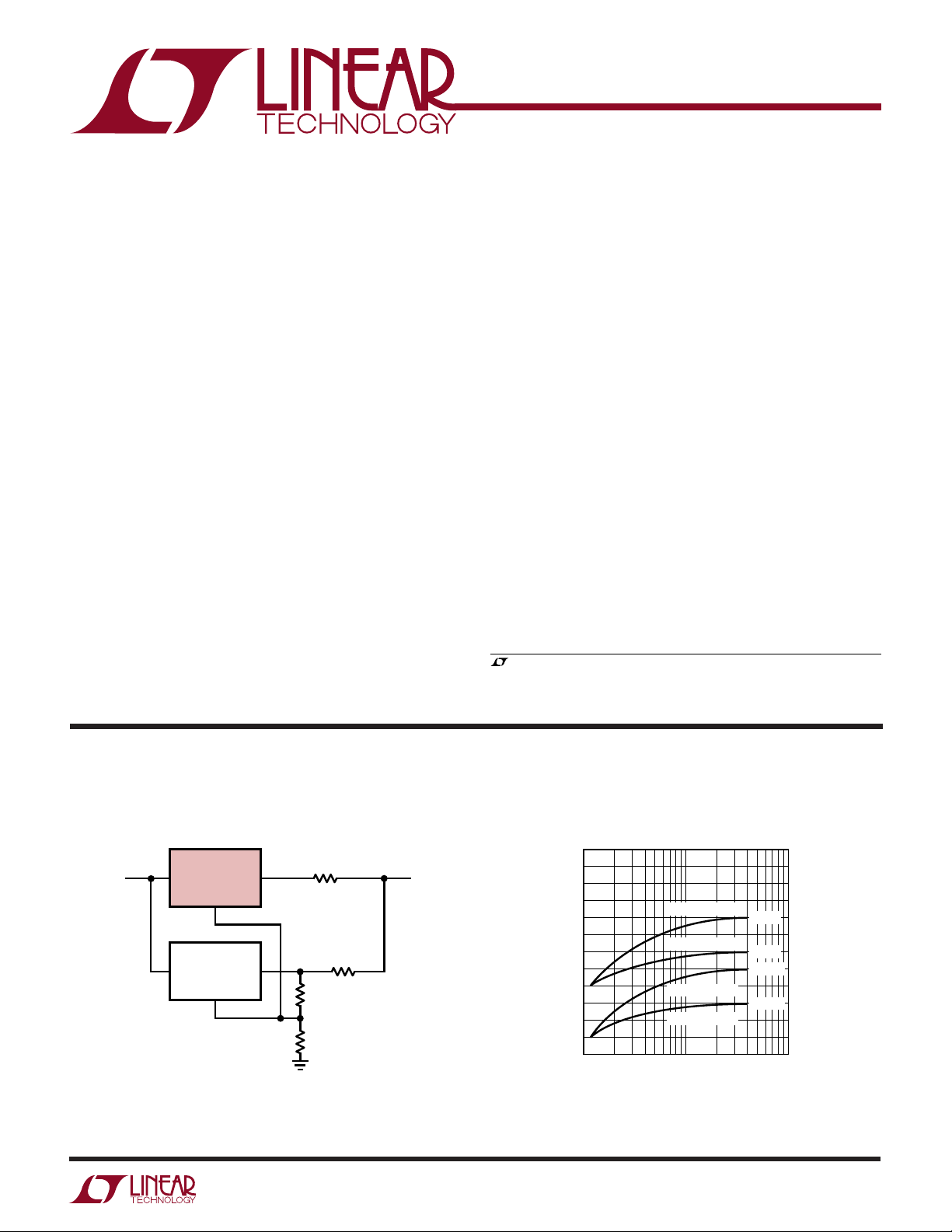
TYPICAL APPLICATIO
V
IN
THIS CIRCUIT WILL NOT WORK WITH LM VERSION DEVICES
*
CURRENT SHARING RESISTORS DEGRADE REGULATION TO 1%
**
U
Parallel Regulators for Higher Current*
LT338A
V
IN
V
IN
V
ADJ
LT350A
V
ADJ
OUT
OUT
0.01Ω**
0.016Ω**
121Ω
1%
365Ω
1%
138/338 TA01
The graph below shows the significant improvement in
output voltage tolerance achieved by using the LT138A or
LT338A.
, LTC and LT are registered trademarks of Linear Technology Corporation.
Output Voltage Error
5V
8A
1
Page 2
LT138A/LT338A
LM138/LM338
A
W
O
LUTEXI TIS
S
A
WUW
U
(Note 1)
ARB
G
Power Dissipation.............................. Internally Limited
Input-to-Output Voltage Differential........................ 35V
Operating Junction Temperature Range
LT138A/LM138 ............................... –55°C to 150°C
LT338A/LM338 ................................... 0°C to 125°C
WU
/
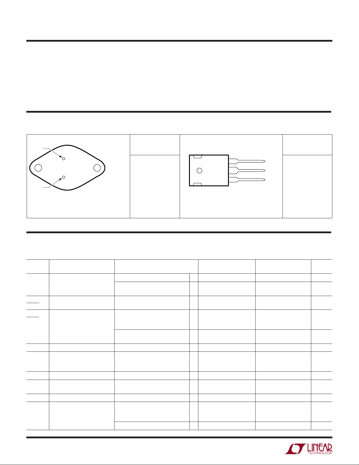
PACKAGE
V
IN
ADJ
2-LEAD TO-3 METAL CAN
T
= 150°C, θ
JMAX
= 125°C, θ
T
JMAX
O
BOTTOM VIEW
2
1
K PACKAGE
= 35°C/ W, θ
JA
= 35°C/ W, θ
JA
RDER I FOR ATIO
ORDER
PART NUMBER
CASE
IS OUTPUT
= 1°C/ W (LT138A/LT138)
JC
= 1°C/ W (LT338A/LT338)
JC
LT138AK
LT338AK
LM138K
LM338K
Storage Temperature Range ................ – 65°C to 150°C
Lead Temperature (Soldering, 10 sec)................. 300°C
UUU
PRECONDITIONI G
100% Thermal Limit Burn-In
U
ORDER
FRONT VIEW
3
2
1
P PACKAGE
3-LEAD PLASTIC TO-3P
T
JMAX
= 125°C, θ
= 45°C/W
JA
V
V
ADJ
PART NUMBER
OUT
IN
LM338P
Consult factory for Industrial grade parts.
ELECTRICAL CHARACTERISTICS
The ● denotes specifications which apply over the full operating
temperature range, otherwise specifications are at TA = 25°C. (Note 2)
SYMBOL PARAMETER CONDITIONS MIN TYP MAX MIN TYP MAX UNITS
V
∆V
∆V
∆V
∆I
I
ADJ
∆I
I
SC
REF
OUT
IN
OUT
OUT
ADJ
Reference Voltage I
Line Regulation 3V ≤ (VIN – V
Load Regulation 10mA ≤ I
Thermal Regulation 20ms Pulse 0.002 0.01 0.002 0.01 %/W
Ripple Rejection V
Adjust Pin Current ● 45 100 45 100 µA
Adjust Pin Current Change 10mA ≤ I
Minimum Load Current (VIN – V
Current Limit (VIN – V
= 10mA, TJ = 25°C 1.238 1.250 1.262 V
OUT
3V ≤ (VIN – V
10mA ≤ I
V
≤ 5V 5 15 5 15 mV
OUT
≥ 5V 0.1 0.3 0.1 0.3 %
V
OUT
V
≤ 5V ● 20 30 20 30 mV
OUT
≥ 5V ● 0.3 0.6 0.3 0.6 %
V
OUT
= 10V, f = 120Hz
OUT
= 0µF ● 60 60 dB
C
ADJ
= 10µF ● 60 75 60 75 dB
C
ADJ
3V ≤ (VIN – V
DC ● 58 58 A
0.5ms Peak
(VIN – V
) ≤ 35V, ● 1.225 1.250 1.270 1.19 1.24 1.29 V
OUT
≤ 5A, P ≤ 50W
OUT
) ≤ 35V, (Note 3) 0.005 0.01 0.005 0.01 %/V
OUT
≤ 5A, (Note 3)
OUT
≤ 5A, ● 0.2 5 0.2 5 µA
OUT
) ≤ 35V
OUT
) = 35V ● 3.5 5 3.5 5 mA
OUT
) ≤ 10V
OUT
) = 30V, TJ = 25°C121A
OUT
● 0.02 0.04 0.02 0.04 %/V
● 612 612 A
LT138A LM138
2
Page 3
LT138A/LT338A
LM138/LM338
ELECTRICAL CHARACTERISTICS
The ● denotes specifications which apply over the full operating
temperature range, otherwise specifications are at TA = 25°C. (Note 2)
LT138A LM138
SYMBOL PARAMETER CONDITIONS MIN TYP MAX MIN TYP MAX UNITS
∆V
OUT
Temperature Stability ● 12 1 %
∆Temp
∆V
OUT
Long-Term Stability TA = 125°C, 1000 Hours 0.3 1 0.3 1 %
∆Time
e
n
θ
JC
RMS Output Noise (% of V
) 10Hz ≤ f ≤ 10kHz 0.001 0.003 %
OUT
Thermal Resistance K Package 1 1 °C/W
Junction-to-Case
The ● denotes specifications which apply over the full operating temperature range,
otherwise specifications are at TA = 25°C. (Note 2)
LT338A LM338
SYMBOL PARAMETER CONDITIONS MIN TYP MAX MIN TYP MAX UNITS
V
REF
∆V
OUT
∆V
IN
∆V
OUT
∆I
OUT
I
ADJ
∆I
ADJ
I
SC
∆V
OUT
∆Temp
∆V
OUT
∆Time
e
n
θ
JC
Reference Voltage I
Line Regulation 3V ≤ (VIN – V
Load Regulation 10mA ≤ I
= 10mA 1.238 1.250 1.262 V
OUT
3V ≤ (VIN – V
10mA ≤ I
V
≤ 5V 5 15 5 25 mV
OUT
V
≥ 5V 0.1 0.3 0.1 0.5 %
OUT
V
≤ 5V ● 20 30 20 50 mV
OUT
≥ 5V ● 0.3 0.6 0.3 1 %
V
OUT
) ≤ 35V, ● 1.225 1.250 1.270 1.19 1.24 1.29 V
OUT
≤ 5A, P ≤ 50W
OUT
) ≤ 35V, (Note 3) 0.005 0.01 0.005 0.03 %/V
OUT
≤ 5A, (Note 3)
OUT
● 0.02 0.04 0.02 0.06 %/V
Thermal Regulation 20ms Pulse 0.002 0.02 0.002 0.02 %/W
Ripple Rejection V
= 10V, f = 120Hz
OUT
C
= 0µF ● 60 60 dB
ADJ
= 10µF ● 60 75 60 75 dB
C
ADJ
Adjust Pin Current ● 45 100 45 100 µA
Adjust Pin Current Change 10mA ≤ I
3V ≤ (V
Minimum Load Current (VIN – V
Current Limit (VIN – V
DC
≤ 5A, ● 0.2 5 0.2 5 µA
OUT
– V
IN
) ≤ 35V
OUT
) = 35V ● 3.5 10 3.5 10 mA
OUT
) ≤ 10V
OUT
● 58 58 A
0.5ms Peak ● 612 612 A
(VIN – V
) = 30V, TJ = 25°C121A
OUT
Temperature Stability ● 12 1 %
Long-Term Stability TA = 125°C, 1000 Hours 0.3 1 0.3 1 %
RMS Output Noise (% of V
) 10Hz ≤ f ≤ 10kHz 0.001 0.003 %
OUT
Thermal Resistance K Package 1 1 °C/W
Junction-to-Case
Note 1: Absolute Maximum Ratings are those values beyond which the life
of the device may be impaired.
Note 2: Unless otherwise specified, these specifications apply:
V
– V
IN
= 5V and I
OUT
= 2.5A. These specifications are applicable for
OUT
power dissipations up to 50W.
Note 3: See thermal regulation specifications for changes in output voltage
due to heating effects. Load and line regulation are measured at a constant
junction temperature by low duty cycle pulse testing.
3
Page 4
LT138A/LT338A
TEMPERATURE (°C)
–75
ADJUSTMENT CURRENT (µA)
35
40
45
75
65
138A/338A G03
30
–25 25 125
50
55
60
LM138/LM338
UW
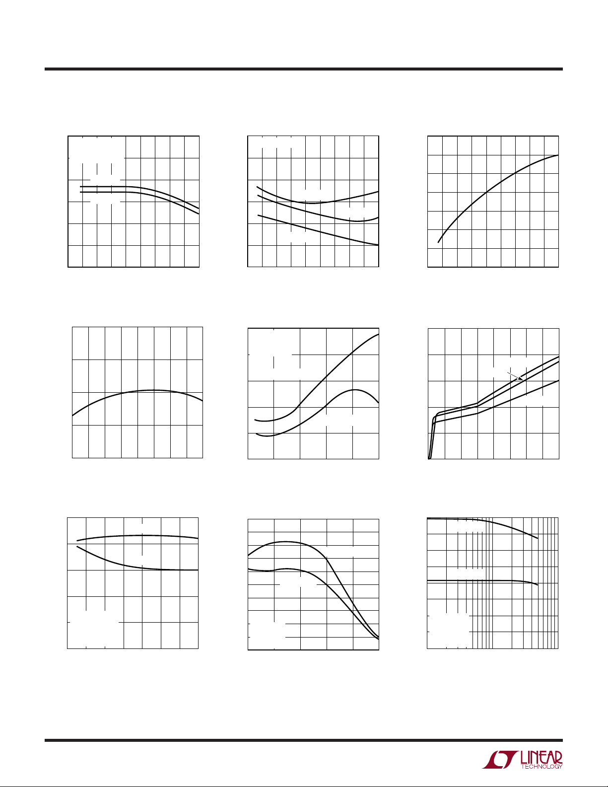
TYPICAL PERFOR A CE CHARACTERISTICS
Load RegulationLoad Regulation
0.2
= 15V
V
IN
V
= 10V
OUT
0.1
PRELOAD = 50mA
I
0
–0.1
–0.2
–0.3
OUTPUT VOLTAGE DEVIATION (%)
–0.4
–75
= 3A
OUT
I
= 5A
OUT
–50 0
–25
TEMPERATURE (°C)
50 150
25
Temperature Stability
1.270
1.260
1.250
1.240
REFERENCE VOLTAGE (V)
Dropout Voltage
4
= 100mV
∆V
OUT
3
I
= 5A
OUT
I
= 3A
2
I
= 1A
INPUT-OUTPUT DIFFERENTIAL (V)
100
125
75
138/338 G01
1
–75
–50 0
OUT
–25
25
TEMPERATURE (°C)
50 150
OUT
100
125
75
138/338 G02
Adjustment Current
Output Impedance Minimum Operating Current
0.1
0.01
OUTPUT IMPEDANCE (Ω)
0.001
10
1
VIN = 15V
= 10V
V
OUT
I
= 500mA
OUT
= C
OUT
= 0µF
C
ADJ
= C
OUT
= 10µF
C
ADJ
5
4
3
2
QUIESCENT CURRENT (mA)
1
TJ = 25°C
= 150°C
T
J
T
= –55°C
J
1.230
–50
–25 0 25 50
TEMPERATURE (°C)
75 100 125 150
138A/338A G04
0.0001
100
10
FREQUENCY (Hz)
10k
100k
1k
1M
138/338 G05
0
0
510
15 25 40
INPUT-OUTPUT DIFFERENTIAL (V)
20
30 35
138A/338A G06
Ripple Rejection Ripple RejectionRipple Rejection
100
C
= 10µF
ADJ
80
C
= 0µF
60
40
RIPPLE REJECTION (dB)
VIN – V
20
0
OUT
I
= 500mA
OUT
f = 120Hz
= 25°C
T
J
05
ADJ
= 5V
20
15
10
OUTPUT VOLTAGE (V)
25
30
138A/338A G07
35
100
80
60
40
RIPPLE REJECTION (dB)
20
VIN = 15V
V
I
0
10
OUT
OUT
= 10V
= 0.2A
100
C
ADJ
C
ADJ
= 0µF
10k
1k
FREQUENCY (Hz)
= 10µF
100k
1M
138A/338A G08
80
70
60
RIPPLE REJECTION (dB)
50
40
V
V
f = 120Hz
T
0.1
C
= 10µF
ADJ
C
ADJ
= 15V
IN
= 10V
OUT
= 25°C
CASE
OUTPUT CURRENT (A)
= 0µF
110
138/338 G09
4
Page 5

UW
TYPICAL PERFOR A CE CHARACTERISTICS
Current Limit Current LimitCurrent Limit
16
12
8
OUTPUT CURRENT (A)
4
0
0
10
INPUT-OUTPUT DIFFERENTIAL (V)
PEAK CURRENT LIMIT
DC CURRENT LIMIT
= 25°C
T
CASE
PRELOAD = 0A
PRELOAD = 5A
PRELOAD = 1A
20
30
138A/338A G10
40
14
12
10
PRELOAD = 5A
8
6
4
OUTPUT CURRENT (A)
VIN = 10V
2
= 5V
V
OUT
= 25°C
T
CASE
0
0.1
PRELOAD = 0A
1 10 100
TIME (ms)
138A/338A G11
LT138A/LT338A
LM138/LM338
14
12
10
8
6
4
OUTPUT CURRENT (A)
2
0
0.1
PRELOAD CURRENT = 0
T
= 25°C
CASE
VIN – V
VIN – V
VIN – V
VIN – V
1 10 100
TIME (ms)
= 10V
OUT
= 15V
OUT
= 20V
OUT
= 30V
OUT
138A/338A G12
Line Transient Response
1.5
V
= 10V
OUT
I
1.0
0.5
–0.5
DEVIATION (V)
OUTPUT VOLTAGE
–1.0
–1.5
1.0
0.5
CHANGE (V)
INPUT VOLTAGE
= 50mA
OUT
T
= 25°C
J
0
0
0
CL = 1µF
C
= 10µF
L
C
C
10 40
U
20 30
TIME (µs)
138A/338A G13
WUU
OUT
ADJ
= 0
= 0
APPLICATIONS INFORMATION
General
The LT138A develops a 1.25V reference voltage between
the output and the adjustable terminal (see Figure 1). By
placing a resistor, R1, between these two terminals, a constant current is caused to flow through R1 and down through
R2 to set the overall output voltage. Normally this current
is the specified minimum load current of 5mA or 10mA.
Because I
with the current through R1, it represents a small error and
can usually be ignored. It is easily seen from the output
voltage equation, that even if the resistors were of exact
value, the accuracy of the output is limited by the accuracy
of V
REF
is very small and constant when compared
ADJ
. Earlier adjustable regulators had a reference
Load Transient Response
3
2
CL = 1µF
= 10µF
C
ADJ
1
0
–1
DEVIATION (V)LOAD CURRENT (A)
OUTPUT VOLTAGE
–2
–3
6
4
2
0
010
CL = 0
= 0
C
ADJ
VIN = 15V
= 10V
V
OUT
= 25°C
T
CASE
PRELOAD = 100mA
20 40
TIME (µs)
30
138A/338A G14
tolerance of ±4% which is dangerously close to the ±5%
supply tolerance required in many logic and analog systems. Further, even 1% resistors can drift 0.01%/°C, adding additional error to the output voltage tolerance.
LT338A
V
IN
V
IN
+
I
ADJ
50µA
V
= V
OUT
Figure 1. Basic Adjustable Regulator
V
OUT
ADJ
1 + + I
REF
()
V
REF
R2
• R2
ADJ
R1
R1
R2
138A/338A F01
V
OUT
5
Page 6

LT138A/LT338A
LM138/LM338
U
WUU
APPLICATIONS INFORMATION
For example, using 2% resistors and ±4% tolerance for
V
, calculations will show that the expected range of a
REF
5V regulator design would be 4.66V ≤ V
approximately ±7%. If the same example were used for a
15V regulator, the expected tolerance would be ±8%. With
these results most applications required some method of
trimming, usually a trim pot. This solution is both expensive and not conductive to volume production.
One of the enhancements of Linear Technology’s adjustable regulators over existing devices is the tightened
initial tolerance of V
. This allows relatively inexpen-
REF
sive 1% or 2% film resistors to be used for R1 and R2 to
set the output voltage within an acceptable tolerance.
With a guaranteed 1% reference, a 5V power supply
design, using ±2% resistors, would have a worst-case
manufacturing tolerance of ±4%. If 1% resistors are used,
the tolerance will drop to ±2.5%. A plot of the worst-case
output voltage tolerance as a function of resistor tolerance
is shown on the front page of this data sheet.
For convenience, a table of standard 1% resistor values is
shown in Table 1.
Table 1. 0.5% and 1% Standard Resistance Values
1.00 1.47 2.15 3.16 4.64 6.81
1.02 1.50 2.21 3.24 4.75 6.98
1.05 1.54 2.26 3.32 4.87 7.15
1.07 1.58 2.32 3.40 4.99 7.32
1.10 1.62 2.37 3.48 5.11 7.50
1.13 1.65 2.43 3.57 5.23 7.68
1.15 1.69 2.49 3.65 5.36 7.87
1.18 1.74 2.55 3.74 5.49 8.06
1.21 1.78 2.61 3.83 5.62 8.25
1.24 1.82 2.67 3.92 5.76 8.45
1.27 1.87 2.74 4.02 5.90 8.66
1.30 1.91 2.80 4.12 6.04 8.87
1.33 1.96 2.87 4.22 6.19 9.09
1.37 2.00 2.94 4.32 6.34 9.31
1.40 2.05 3.01 4.42 6.49 9.53
1.43 2.10 3.09 4.53 6.65 9.76
Standard resistance values are obtained from the Decade Table by
multiplying by multiples of 10. As an example, 1.21 can represent 1.21Ω,
12.1Ω, 121Ω, 1.21k etc.
Bypass Capacitors
Input bypassing using a 1µF tantalum or 25µf electrolytic
is recommended when the input filter capacitors are more
than 5 inches from the device. Improved ripple rejection
≤ 5.36V or
OUT
(80dB) can be accomplished by adding a 10µF capacitor
from the ADJ pin to ground. Increasing the size of the
capacitor to 20µF will help ripple rejection at low output
voltage since the reactance of this capacitor should be
small compared to the voltage setting resistor, R2. For
improved AC transient response and to prevent the possibility of oscillation due to unknown reactive load, a 1µF
capacitor is also recommended at the output. Because of
their low impedance at high frequencies, the best type of
capacitor to use is solid tantalum.
Protection Diodes
The LT138A/LT338A do not require a protection diode
from the adjustment terminal to the output (see Figure 2).
Improved internal circuitry eliminates the need for this
diode when the adjustment pin is bypassed with a capacitor to improve ripple rejection.
If a very large output capacitor is used, such as a 100µF
shown in Figure 2, the regulator could be damaged or
destroyed if the input is accidentally shorted to ground or
crowbarred, due to the output capacitor discharging into
the output terminal of the regulator. To prevent this, a
diode D1 as shown, is recommended to safely discharge
the capacitor.
D1
1N4002
LT338A
V
IN
V
V
IN
ADJ
OUT
C
ADJ
10µF
Figure 2
NOT
R1
NEEDED
R2
+
V
C
OUT
100µF
138A/338A F02
OUT
Load Regulation
Because the LT138A is a three-terminal device, it is not
possible to provide true remote load sensing. Load regulation will be limited by the resistance of the wire connecting the regulator to the load. The data sheet specification
for load regulation is measured at the bottom of the
package. Negative side sensing is a true Kelvin connection, with the bottom of the output divider returned to the
6
Page 7

LT138A/LT338A
LM138/LM338
U
WUU
APPLICATIONS INFORMATION
negative side of the load. Although it may not be immediately obvious, best load regulation is obtained when the
top of the resistor divider, R1, is connected
case
not to the load
. This is illustrated in
directly
Figure 3
to the
. If R1
were connected to the load, the effective resistance between the regulator and the load would be:
RR
R
PP
21
+
R
1
R ParasiticLine sis ce
=, Re tan
Connected as shown, RP is not multiplied by the divider
ratio. RP is about 0.004Ω per foot using 16 gauge wire.
This translates to 4mV/ft at 1A load current, so it is
important to keep the positive lead between regulator and
load as short as possible, and use large wire or PC board
traces.
U
TYPICAL APPLICATIONS
R
P
LT338A
ADJ
V
OUT
V
IN
V
IN
PARASITIC
LINE RESISTANCE
CONNECT
R1 TO CASE
R1
R
R2
CONNECT
R2 TO LOAD
138A/338A F03
Figure 3. Connections for Best Load Regulation
L
Improving Ripple Rejection
LT338A
V
IN
+
*C1 IMPROVES RIPPLE REJECTION, X
SHOULD BE SMALL COMPARED TO R2
IN
1µF
ADJ
V
OUT
R1
121Ω
1%
R2
365Ω
1%
C
1.2V to 25V Adjustable Regulator
LT338A
V
IN
*
**
†
V
IN
+
C1*
1µF
NEEDED IF DEVICE IS FAR FROM FILTER CAPACITORS
OPTIONAL, IMPROVES TRANSIENT RESPONSE
V
= 1.25V
OUT
V
OUT
ADJ
R2
5k
R2
1 +
()
R1
R1
240Ω
+
138A/338A TA04
+
138A/338A TA03
V
C2**
1µF
C
10µF
OUT
5VV
*
L
†
7
Page 8

LT138A/LT338A
LM138/LM338
U
TYPICAL APPLICATIONS
Temperature Compensated Lead Acid Battery Charger
5V Regulator with Shutdown
LT338A
1µF
V
IN
ADJ
1k
1k
V
TTL
IN
+
V
OUT
2N3904
5V
121Ω
1%
365Ω
1%
138A/338A TA05
V
RETURN
3A
LT338A
V
IN
2N3906
ADJ
50Ω
V
OUT
243Ω
1%
10k
12V
2k
50k
138A/338A TA07
Remote Sensing
R
P
LT338A
ADJ
V
OUT
25Ω
121Ω
365Ω
7
6
LM301A
1
100pF
V
IN
IN
(MAX DROP
300mV)
V
IN
–
2
1k
+
3
8
5µF
4
V
OUT
5V
R
L
+
25Ω
138A/338A TA06
RETURN
8
Page 9

WW
SCHE ATIC DIAGRA
LT138A/LT338A
LM138/LM338
LT138A/LT338A
IN
V
300Ω
Q24
Q23
200Ω
D1
Q28
Q27
120Ω
Q26
12k
C3
6.7k
Q21
1.6k
Q19
18k
160k
400Ω
5pF
Q22
Q18
16k
D2
Q25
Q20
160Ω
3Ω
2.4k
Q17
12k
OUT
V
138A/338A SS
0.01Ω
ADJ
+
C2
C1
20k5.6k50Ω190Ω310Ω310Ω
30pF
30pF
+
Q14
3k
Q16
5.1k4.1k
Q15
Q13
Q1
Q9
Q6Q4
Q2
12.4k
4k
Q5
30k
Q12
Q10
Q11
Q8
130Ω
Q1
10Ω4.1k180Ω
Q7
Q3
160k
9
Page 10

LT138A/LT338A
LM138/LM338
PACKAGE DESCRIPTION
U
Dimensions in inches (millimeters) unless otherwise noted.
K Package
2-Lead TO-3 Metal Can
(LTC DWG # 05-08-1310)
0.320 – 0.350
(8.13 – 8.89)
0.420 – 0.480
(10.67 – 12.19)
0.210 – 0.220
(5.33 – 5.59)
0.425 – 0.435
(10.80 – 11.05)
0.067 – 0.077
(1.70 – 1.96)
0.760 – 0.775
(19.30 – 19.69)
0.038 – 0.043
(0.965 – 1.09)
1.177 – 1.197
(29.90 – 30.40)
0.060 – 0.135
(1.524 – 3.429)
0.655 – 0.675
(16.64 – 17.15)
0.490 – 0.510
(12.45 – 12.95)
R
0.151 – 0.161
(3.86 – 4.09)
DIA, 2PLCS
0.167 – 0.177
(4.24 – 4.49)
R
K2 (TO-3) 1098
10
Page 11

PACKAGE DESCRIPTION
LT138A/LT338A
LM138/LM338
U
Dimensions in inches (millimeters) unless otherwise noted.
P Package
3-Lead Plastic TO-3P (Similar to TO-247)
(LTC DWG # 05-08-1450)
0.560
(14.224)
0.325
(8.255)
BOTTOM VIEW OF TO-3P
HATCHED AREA IS SOLDER PLATED
COPPER HEAT SINK
0.580
(14.732)
(17.780)
0.124
(3.149)
0.275
(6.985)
0.700
0.098
(2.489)
0.830 – 0.870
(21.08 – 22.10)
0.580 – 0.6OO
0.580 – 0.6OO
(14.73 – 15.24)
(14.73 – 15.24)
0.780 – 0.800
(19.81 – 20.32)
0.042 – 0.052
(1.07 – 1.32)
0.170
(4.32)
MAX
0.074 – 0.084
(1.88 – 2.13)
0.620 – 0.64O
0.620 – 0.64O
(15.75 – 16.26)
(15.75 – 16.26)
0.215
(5.46)
BSC
0.113 – 0.123
(2.87 – 3.12)
MOUNTING HOLE
0.115 – 0.145
(2.92 – 3.68)
DIA
0.170 – 0.2OO
(4.32 – 5.08)
EJECTOR PIN MARKS
0.105 – 0.125
(2.67 – 3.18)
DIA
18° – 22°
3° – 7°
0.187 – 0.207
(4.75 – 5.26)
0.060 – 0.080
(1.52 – 2.03)
0.087 – 0.102
(2.21 – 2.59)
0.020 – 0.040
(0.51 – 1.02)
P3 0996
Information furnished by Linear Technology Corporation is believed to be accurate and reliable.
However, no responsibility is assumed for its use. Linear Technology Corporation makes no representation that the interconnection of its circuits as described herein will not infringe on existing patent rights.
11
Page 12

LT138A/LT338A
LM138/LM338
U
TYPICAL APPLICATIONS
15V
Lamp Flasher
LT338A
V
+
1k
IN
1µF
OFF
2N3904
ADJ
12k
12k
12k
V
OUT
10µF
10µF
10µF
+
+
+
12V
138A/338A TA08
Automatic Light Control
LT338A
V
IN
ADJ
V
OUT
1.2k
138A/338A TA09
Protected High Current Lamp Driver
15V
12V
5A
TTL OR
CMOS
LT338A
ADJ
V
IN
V
OUT
10k
138A/338A TA10
RELATED PARTS
PART NUMBER DESCRIPTION COMMENTS
LT1084 5A Low Dropout Operates to 30V Input
LT1580 7A Fast Transient Response Regulator with 0.7V Dropout For 3.3V to 2.xxV Applications
LT1581 10A Fast Transient Response Regulator For 3.3V to 2.xxV Applications
LT1585/LT1587 7A/4.6A/3A Low Dropout Fast Transient Response Regulator For 1.2V to 3.3V Outputs from 5V
12
Linear T echnology Corporation
1630 McCarthy Blvd., Milpitas, CA 95035-7417
(408) 432-1900 ● FAX: (408) 434-0507
●
www.linear-tech.com
138afa LT/LT 1199 2K REV A • PRINTED IN THE USA
LINEAR TECHNOLOGY CORPORATION 1991
 Loading...