

Page 1
PREPARED BY:
DATE:
A-
t SPEC.No: DG-996011
APPROVED BY: DATE: ELECTRONIC COMPONENTS GROUP
Jd B /‘YY
( SPECIFICATION 1 Opto-Electronic Devices Division
/
DEVICE SPECIFICATION FOR
SHARP CORPORATION
REPRESENTATIVE DIVISION:
Y
.
Light Emitting Diode
MODEL No.
LTlZE4OA
1. These specification sheets include materials protected under the copyright of Sharp Corporation (“Sharp”).
Please do not reproduce or cause anyone to reproduce them without Sharp5 consent.
2. When using this product, please observe the absolute maximum ratings and the instructions for use outlined
in these specification sheets, as well as the precautions mentioned below. Sharp assumes no responsibility
for any damage resulting corn use of the product which does not comply with the absolute maximum ratings
and the instructions included in these specification sheets, and the precautions mentioned below.
(Precautions)
(1) This products is designed for use in the following application areas;
* OA equipment * Audio visual equipment * Home appliance
* Telecommunication equipment (Terminal) * Measuring equipment
* Tooling machines * Computers
I
If the use of the product in the above application areas is for equipment listed in paragraphs
(2) or (3), please be sure to observe the precautions given in those respective paragraphs.
(2) Appropriate measures, such as fail-safe design and redundant design considering
the safety design of the overall system and equipment, should be taken to ensure reliability
and safety when this product is used for equipment which demands high reliability and
safety in function and precision, such as ;
* Transportation control and safety equipment (aircraft, train, automobile etc.)
* Traffic signals * Gas leakage sensor breakers l Rescue and security equipment
* Other safety equipment
L
(3) Please do not use this product for equipment which require extremely high reliability
and safety in fimction and precision, such as ;
* Space equipment * Telecommunication equipment (for trunk lines)
l
Nuclear power control equipment * Medical equipment
c
. (4) Please contact and consult with a Sharp sales representative if there are any questions
regarding interpretation of the above three paragraphs.
-I
1
1
1
3. Please contact and consult with a Sharp sales representative for any questions about this product.
DATE:
CUSTOMER’S APPROVAL
DATE:
BY:
PRESENTED BY:
M.Katoh,
Department General Manager of
Engineering Dept.,111
Opto-Electronic Devices Division
Electronic Components Group
SHARP CORPORATION
I
Page 2
J .i L.
i __,
MODEL Nd. ‘- _. -
LTlZE40A Smdkation
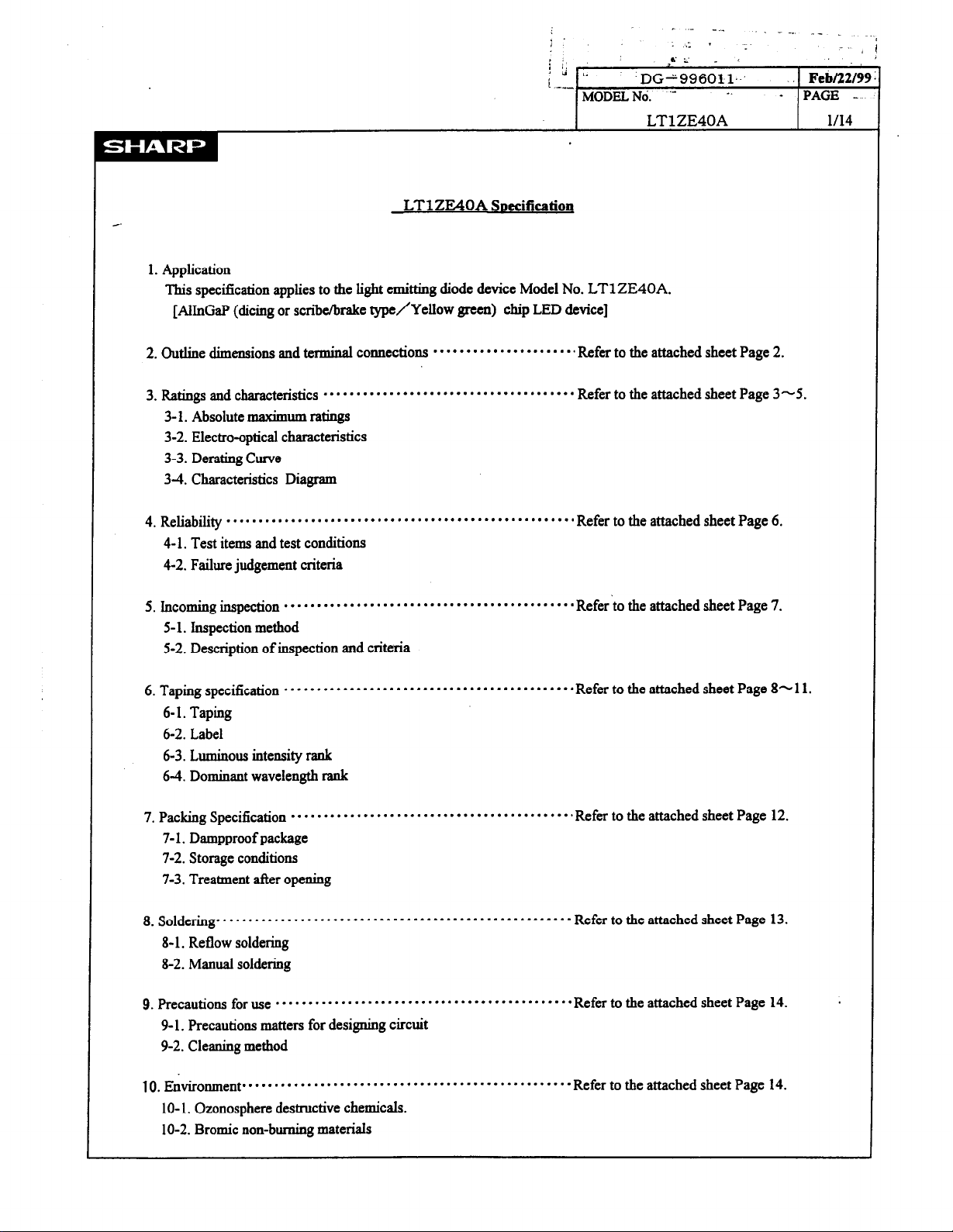
1. Application
This specification applies to the light emitting diode device Model No. LTl ZE4OA.
[AlInGaP (dicing or scribe/brake type/Yellow green) chip LED device]
.DG-g96011.-. . Feb/22/9!
PAGE -
LTl ZE40A l/14
2. Outline dimensions and temkal connections
3. Ratings and characteristics
. . . . . . . . . . . . . . . . . . . . . . . . . . . . . . . . . . . . . .
3- 1. Absolute maximum ratings
3-2. Electra-optical characteristics
3-3. Derating Curve
3-4. Characteristics Diagram
4. Reliability
. . . . . . . . . . . . . . . . . . . . . . . . . . . . . . . . . . . . . . . . . . . . . . . . . . . . .
4-1. Test items and test conditions
4-2. Failure judgement criteria
5. incoming inspection
. . . . . . . . . . . . . . . . . . . . . . . . . . . . . . . . . . . . . . . . . . . .
5- 1. Inspection method
5-2. Description of inspection and criteria
6. Taping specification
. . . . . . . . . . . . . . . . . . . . . . . . . . . . . . . . . . . . . . . . . . . .
6-1. Taping
6-2. Label
6-3. Luminous intensity rank
6-4. Dominant wavelength raak
...*.*..**...~.......,~f~ to the attached sheet Page2.
Refer to the attached sheet Page 3-5.
Refer to the attached sheet Page 6.
Refer to the attached sheet Page 7.
Refer to the attached sheet Page 8- 11.
7. Packing Specification
. . . . . . . . . . . . . . . . . . . . . . . . . . . . . . . . . . . . . . . ...*
7- 1. Dampproof package
7-2. Storage conditions
7-3. Treatment after opening
8. Soldering
. . . . . . . . . . . . . . . . . . . . . . . . . . . . . . . . . . . . . . . . . . . . . . . . . . . . . .
8- 1. Reflow soldering
8-2. Manual soldering
9. Precautions for use
. . . . . . . . . . . . . . . . . . . . . . . . . . . . . . . . . . . . . . . . . . . . .
9- 1. Precautions matters for designing circuit
9-2. Cleaning method
10. Ekironment
. . . . . . . . . . . . . . . . . . . . . . . . . . . . . . . . . . . . . . . . . . . . . . . . . .
lo- 1. Ozonosphere destructive chemicals.
10-2. Bromic non-burning materials
Refer to the attached sheet Page 12.
Refer to the attached sheet Page 13.
Refer to the attached sheet Page 14.
Refer to the attached sheet Page 14.
Page 3
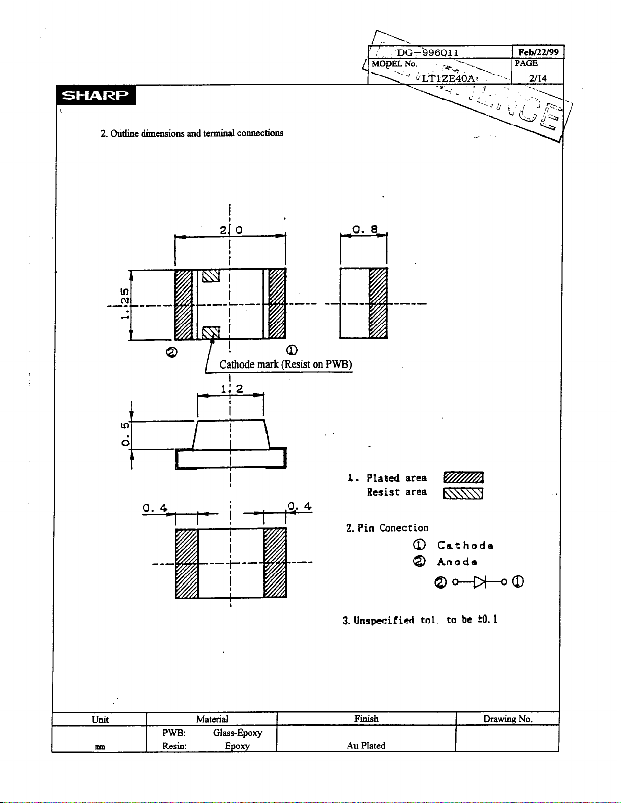
2. Outliue dimensions and terminal connections
Febl2219’
unit
mm
j---
0. 4 .
I I- h-l=
.
---
Material
PWB: Glass-Epoxy
Resin:
I
Epoxy
1. Plabzd area m
Resist area m
2. Pin Conection
0 Cathode
e-w
@ Anode
43-o
3. Unspecified tol. to be ktl. 1
Finish
Au Plated
Drawiug No.
Page 4
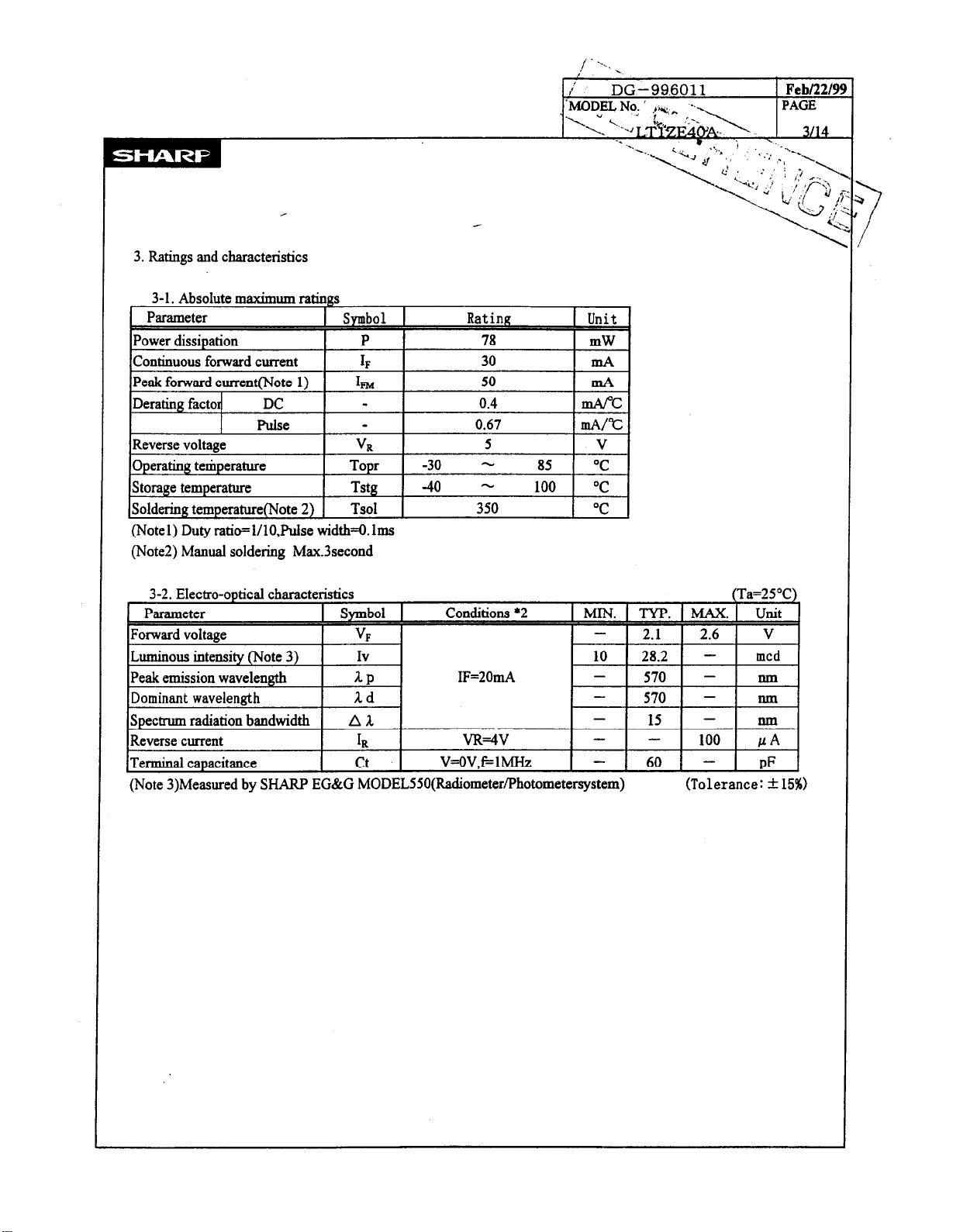
3. Ratings and characteristics
/ _.. _
/
I
DG-99.6011
ifDDEl, No. ’ ,,-, _
-‘.
‘-\U \.‘yi t * :.-- \
-.
.._
. . .
Febl22/99-
PAGE
3/14
(Notel) Duty ratio=l/lO,Puise width=O.lms
(Note2) Manual soldering Max.3second
(Note 3)Measured by SHARP EG&G MODELSSO(Radiometer/Photometersystem) (Tolerance: f 15%)
L
Page 5
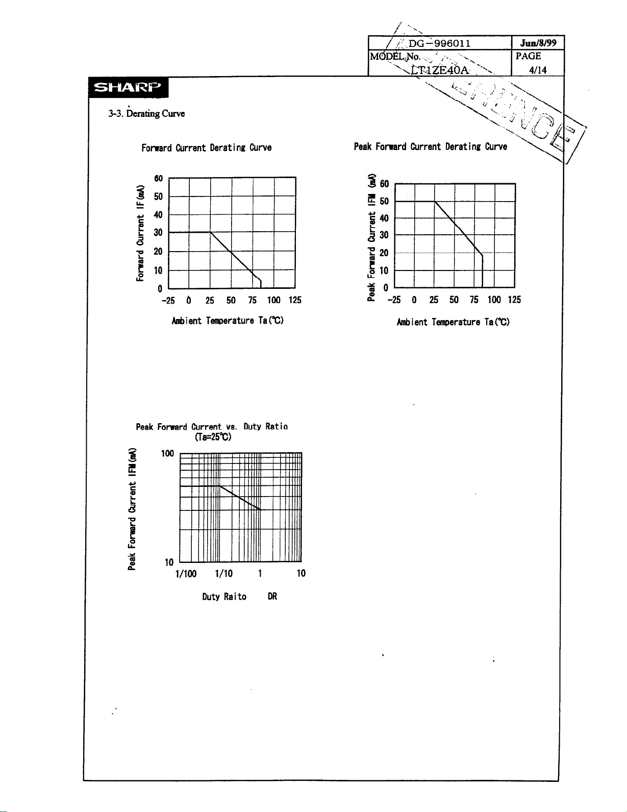
Forward Current Derating Curve
60
-25 b 25 50
Anbient Temperature Ta("c)
Peak Fotward Current vs. Duty Ratio
cTa=25"c)
l/100 l/10 1
Duty Raito DR
75 100 125
10
Page 6

(/ ’ ~ dG-996011 1 Jud8/9!
MopLyo.., .. \\
’ -.LT l,$EdO A~,
‘, ._ 5114
PAGE
3-4. Characteristics Diagram(typ)
Forward Current vs.Fotward Voltage
s
E
a
Y
t
2
l.L
0.
1 1.2 1.4 1.6 1.8 2 2.2 2.4
Fotward Voltage VFW
(Note
1)
fla=2573
Relative Luminous Intensity
vs. Ambient Tamerature
1000
8
B
-60 -40 -20 0 20 40 60 80 100 120
Ambient Tetwature Ta("c)
(IF=5mAI
Relative Lminoua lntenaitv VI. Fromrd Voltare
Ua=25%)
t
i i iiitttt i i iii/iii i i iiiiltl
0. 1 1 10 100
Forward Current IFW
(Note 1) Above characteristic data are typical data and not a guarantteed data.
Page 7

4. Reliability
The reliability of products shall be satisfied with items listed below.
,-I. Test items and test conditions Confidence level: 907
4-2. Failure judgement criteria * 1
Parameter Symbol
Forward voltage
Reverse current
Luminous intensity
l
1: Measuring condition is in accordance with specification.
vF
IR
IV
Iv > The first stage value X 2.0 or The first stage value X 0.5 > Iv
$2: U.S.L. is shown by Upper Specification Limit.
Failure judgement criteria l 2
v, > U.S.L. x 1.2
IR > U.S.L. x 2.0
Page 8

i I.
, I,. ., “k.
JIG<-9960‘1 1
/
*-YODEL No.,,.
y ~hZk40~-..
5. Incoming inspection
S- 1. Inspection method
A single sampling plan, normal inspection level S-4 based on IS0 2859-l shall be adopted.
) ‘I. .,
Febl22/9!
PAGE
7114
AQL
Product inserted in reverse direction
7
Outline dimensions
8 Dust and flaw
Not conforming to the specification
Effect to the specification
9 Resin flash Over the unspecified tolerance
10 Resin crack 0.3mm or greater Corn the product side face
11 Solderbility
could solder 50% or greater and less than 90% out of
judgement area * 1
* 1 Judgement area : The plated area of the product bottom
Minor
defect
0.1%
0.4%
Page 9

6.Taping specification
6-l.Tapiug
6-1-l.Shape and dimension of tape(TYP.)
w
tP Cathode 1
Cover tape
Carrier tape Width
Thickness of the entire unit t2 1.2
% Material : Carrier tape...PS, Cover tape.. . Polyester
Width
Thickness
Thickness t 1
WI 5.5
t
Wa
3
0.1
8.0
0.2
With cover tape and carrier tape combined
Page 10

6-I-2.Shape and dimension of reel(TYP.)
-._
. .
DG-996011
Febl22/9
PAGE
9114
Parameter 1 Symbol 1 Dimension 1
Frange
External diameter
Hub Spindle hole diameter
Key slit Width
Depth
dotation for part name etc.
% Material : Reel...Polystyrene
Remarks
460
C
E
U
Labeling on one side of flange.(part name,quantity,lot No.)
413
2.0
4.5
Page 11

MO&L go. ..-
6-1-3.Taping specification
(1) Lead tape:
End
(2) Cover tape strength against peeling:F=O. l-O.SN( 6 =lO”or less)
Cover tape
1 ’ - ‘%pe speed : Sum/s
<- Forward Carrier tape
’ I; DG-996011
--Y Ly &&A‘ y..,
40-50 pitch
Febl22/99
PAGE
10114
(3) Tape strength against bending:
The radius of bending circle should be 30mm or more.
If it is less than 3Omm, the cover may peel.
(4) Jointing of tape: There should not be joint of cover tape or carrier tape.
(5) Quantity per reel: Average 4,OOOpcs. per reel
(6) Others:
0 There should not be missing above continuous three products.
@ Products should be easily taken out.
@ Products should not be attached to the cover tape at peeling.
Page 12

6-2.
Label
cl+ Model number -
QUAIiKR
i
i-
c Quantity of products
+ EIAJ C-3 Bar code
0 Production plant code(to be indicated alphabetically)
@ Production lot(single or double figures)
Q) Year of production(tbe last two figures of the year)
@ Month of production
(to be indicated alphabetically with January corresponding to A)
@ Date of production(0 1 - 3 1)
,’ ,: DG-996011
Jud8/9!
M,ODEI, No. <4 “~ PAGE
.A. u ..LTl~Ei~A
1 l/14
6-3.Lurninous intensity rank(Note 1)
Luminous intensity
A 10 -
B
C
D
E
(Note 1)
14 -
21 -
30 43 - 84
Also I sbaIl not ask tbe delivery ratio of each rank.
6-4.Dominant wavelength rank (Note 2)
Dominant wavelength unit
d 562 - 566.0
e
f
(r
565.0 - 569
568 - 572.0
571n - 575
19
28
40
30
unit
mcd
(Ta=25”C)
Condition
J?=2omA
(Ta=25”C)
Condition
(Note 2) This rank value is the setting value of when that cla.ssiiIes it the rank and be not a guarantee value.
Also I shall not ask the delivery ratio of each rank.
Page 13

7. PaclAng specification
7- 1. Dampproof package
In other to avoid the absorption of humidity iu transport and storage,
the device s are packed in aluminum sleeve.
e -
Silicagel
,.’ , . . /
\ _
.-.
Y DGr996011
MODEL For 1 ..v , a; -- .
Label
Febl22199
PAGE
Q
Ree1 Label
7-2.Strage conditions
Temperature : 5 to 30°C Humidity : less than 6O%RH
7-3.Treatment after opening
(1) Please make a soldering within 15 days after opening under following condition;
Temperature : 5 to 30°C Humidity : less than 6O%RH
(2) In case the devices are not used for a long time after opening ,the storage in dry box is recommendable.
Or it is better to repack the devices with a desiccative by the sealer and put them in the some storage
conditions as 7-2. Then they should be used withiu 2 weeks.
(3) Please make a soldering after a follewing bakiug treatment if unused term should be over the conditions
OfW
*Recommendable conditions:
0 in taping
Temprature:6O”c to 65”C,Time:36 to 48 hours
0 in individual (on PWB or metallic tray)
Temprature:lOO”Cto120”C ,Time:2 to 3 hours
Page 14

8. Soldering
8- 1 .Reflow soldering
(1) It is not recommended to exceed the soldering temperature and time shown below.
Caused by substrate bend or the other mechanical stress during reflow soldering
may happen gold wire disconnection etc. Therefore please check and study your
solder reflow machine’s best condition.
(2) In case of 2 times reflow process.2nd reflow process should be done within 8 hours
after 1st reflow process.(Strage condition ; at 3O”c,RH less than 6O%RH) ’
(3) Reflow soldering temperature profile
to be done under the following condition.
MAX 250
Febl22/99
PAGE
13114
140-160
h
Time(s)
Recommendable Thermal Model
(4) Recommendable Metal Mask pattern for screen print
Recommend 0.2mm to 0.3mm thickness metal mask
for screen print. Caused by solder reflow condition,
solder paste, substrate and the other material etc.,
may change solderbility.
Please check and study actual solderbility before
usage.
8-2.Manual soldering
(1) It is recommended to keep the soldering iron temperature at 350% (soldering iron
power consumption 2OW) and not to solder more than once or for over 3 seconds.
(2) When using a soldering iron, care must be taken not to damage the package.
(Pay attention not to allow any under stress or heat on package.)
---mm -.-_-.-_ .-.
R
Recommended soldar pattern (U&mm)
/ 4
‘- - - -. - - -. - . - _ -. -
i
i
il
”
1.25
IF
A
2 , Center of the produc
r
L
L
Page 15

9-l. Precautions matters for designing circuit
This product is not designed as electromagnetic and ionized-particle radiation resistant.
9-2. Cleaning method
(1) Solvent cleaning
Recommend conditions:
(2) Ultrasonic cleaning
The affect on the device from ultrasonic bath, ultrasonic output, duration, board size and device mounting method.
Test the cleaning method under actual conditions and check for abnormalities before actual use.
(3) Solvents
Use only the following types of solvent.
water, methyl alcohol, ethyl alcohol, isopropyl alcohol
Recommend conditions: RT. 4OKHz, 3OW/l, 3 to 5 minutes
10. Environment
10-l. Ozonosphere destructive chemicals.
(1) The device doesn’t contain following substance.
(2) The device doesn’t have a production line whose process requires following substance.
Restricted part: CFCs,halones,CCh,Trichloroethane(Methychlorofotm)
1 O-2. Bromic non-burning materials
The device doesn’t contain bromic non-burning materials(PBBOs,PBBs)
0 Solvent temperature is not more than 45 degree. 0 Immersion up to 3 minutes.
 Loading...