

Page 1
ELECTRONIC COMPONENTS GROUP
SHARP CORPORATION
SPECIFICATION
DEVICE SPECIFICATION FOR
Light Emitting Diode
I
MODELNo.
LTlS9OA
1. These specification sheets include materials protected under the copyright of Sharp Corporation (“Sharp”).
Please do not reproduce or cause anyone to reproduce them without Sharp’s consent.
2. When using this product, please observe the absolute maximum ratings and the instructions for use outlined
in these specification sheets, as well as the precautions mentioned below. Sharp assumes no responsibility
for any damage resulting from use of the product which does not comply with the absolute maximum ratings
and the instructions included in these specification sheets, and the precautions mentioned below.
(Precautions)
(1) This products is designed for use in the following application areas;
* OA equipment * Audio visual equipment * Home appliance
* Telecommunication equipment (Terminal) * Measuring equipment
* Tooling machines * Computers
L
If the use of the product in the above application areas is for equipment listed in paragraphs
(2) or (3), please be sure to observe the precautions given in those respective paragraphs.
(2) Appropriate measures, such as fail-safe design and redundant design considering
the safety design of the overall system and equipment, should be taken to ensure reliability
and safety when this product is used for equipment which demands high reliability and
safety in function and precision, such as ;
* Transportation control and safety equipment (aircraft, train automobile etc.)
* Traflic signals * Gas leakage sensor breakers
* Other safety equipment
i
(3) Please do not use this product for equipment which require extremely high reliability
and safety in timction and precision, such as ;
* Space equipment * Telecommunication equipment (for trunk lines)
* Nuclear power control equipment * Medical equipment
i
(4) Please contact and consult with a Sharp sales representative if there are any questions
regarding interpretation of the above three paragraphs.
* Rescue and security equipment
1
I
3. Please contact and consult with a Sharp sales representative for any questions about this product.
DATE:
CUSTOMERS APPROVAL
DATE:
BY:
PRESENTED BY:
M.Katoh,
Department General Manager of
Engineering Dept.,III
Opto-Electronic Devices Division
Electronic Components Group
SHARP CORPORATION
Page 2
LTlSSOA Sriecification
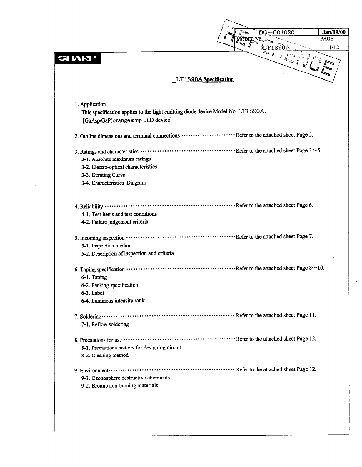
1. Application
This specification applies to the light emitting diode device Model No. LT 1 S 90A.
[GaAsp/GaP(orange)chip LED device]
Jad19lOO
2. Outline dimensions and terminal connections
3. Ratings and characteristics
. . . . . . . . . . . . . . . . . . . . . . . . . . . . . . . . . . . . . . . .
3- 1. Absolute maximum ratings
3-2. Electra-optical characteristics
3-3. Derating Curve
3-4. Characteristics Diagram
4. Reliability
. . . . . . . . . . . . . . . . . . . . . . . . . . . . . . . . . . . . . . . . . . . . . . . . . . . . . . .
4- 1. Test items and test conditions
4-2. Failure judgement criteria
5. Incoming inspection
. . . . . . . . . . . . . . . . . . . . . . . . . . . . . . . . . . . . . . . . . . . . . .
5-l. Inspection method
5-2. Description of inspection and criteria
6. Taping specification
. . . . . . . . . . . . . . . . . . . . . . . . . . . . . . . . . . . . . . . . . . . . . .
6-1. Taping
6-2. Packing specification
6-3. Label
6-4. Luminous intensity rank
. . . . . . . ..***.*.........Refer to the attached sheet Page 2.
Refer to the attached sheet Page 3-5.
Refer to the attached sheet Page 6.
Refer to the attached sheet Page 7.
Refer to the attached sheet Page 8- 10.
7. Soldering
. . . . . . . . . . . . . . . . . . . . . . . . . . . . . . . . . . . . . . . . . . . . . . . . . . . . . . . .
7- 1. Reflow soldering
8. Precautions for use
. . . . . . . . . . . . . . . . . . . . . . . . . . . . . . . . . . . . . . . . . . . . . . .
8-1. Precautions matters for designing circuit
8-2. Cleaning method
9 Env~o~ent.......................................~.............Referto~ea~chedsheetP~e
9-1. Ozonosphere destructive chemicals.
9-2. Bromic non-burning materials
Refer to the attached sheet Page’ 11.
Refer to the attached sheet Page 12.
12.
Page 3
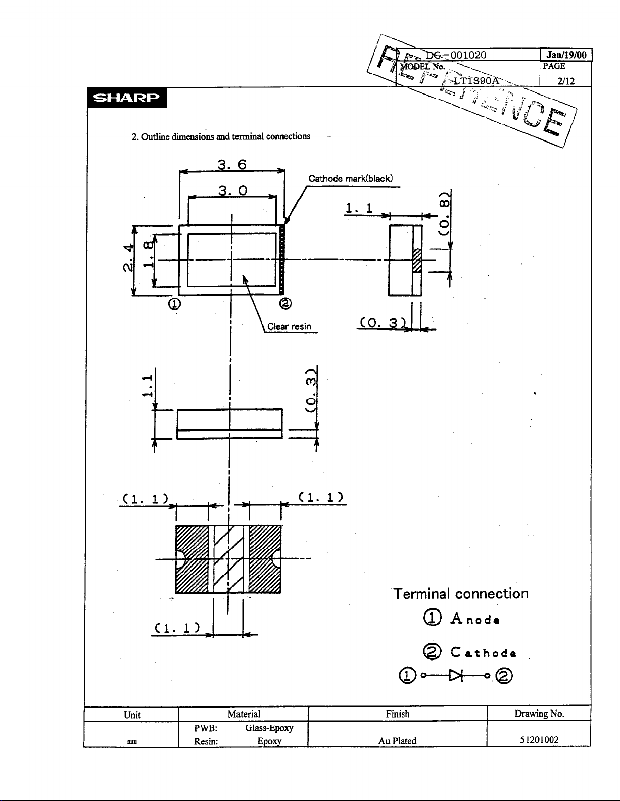
2. Outline dimensi&s and terminal
coMections -
I(
3. 6
Cathode mark(blackl
.
unit
mm
Material
PWB: Glass-Epoxy
Resin:
Epoxy
Terminal connection
0
Anod:
Qc
Finish Drawing No.
Au Plated
athode
51201002
Page 4
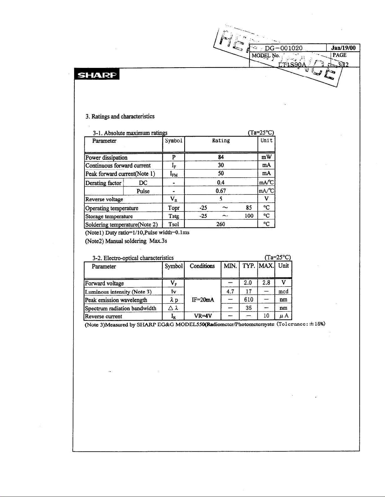
3. Ratings and characteristics
3- 1. Absolute
Parameter Symbol Rating Unit
[Power dissipation P
maximum ratings
IF
(Ta=2S’C)
I
84
30
n-A/T
VR
Topr
Storage temperature Tstg 1 -25 - 100 1 “C
ISoldering temperature(Note 2) 1 Tsol 1 260
(Notel) Duty ratio=l/lO,Pulse width=O. lms
(Note2) Manual soldering Max.3~
-25 - 85
~
1 T 1
mW
mA
mA
V
OC
(Note 3)Measured by SHARP EG&G MODEL5SO(Radiometer/Photometersyste (Tolerance : f 15%)
Page 5
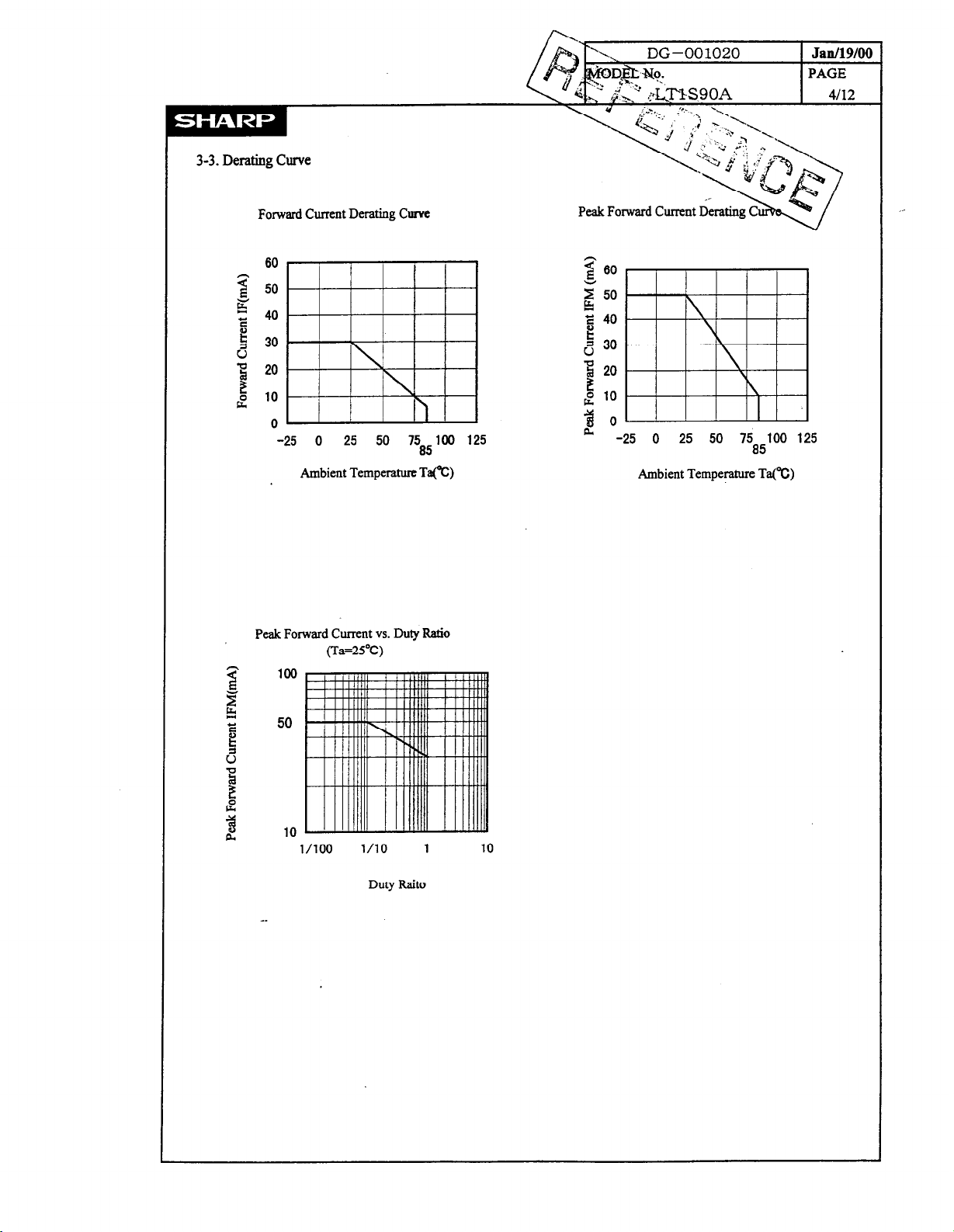
3-3.
Derating Curve
Forward Current Derating Cunz
60
$
50
ic
E 40
g 30
a
$ 20
g 10
0
-25 0 25 50 $5100 125
Ambient Temperahue Ta(“C)
Peak Forward Current vs. Duty Ratio
(Ta=25”C)
$ 60
i 50
z 40
ii
5 30
-g 20
z
g 10
0 25 50 75*5100 125
Ambient Temperature Ta(“c)
l/100
I
l/10
Duty Raito
1 10
Page 6

3-4. Characteristics Diagram(typ) (Note
Jan/19/00
PAGE
5112
--
1000%
9
@
P
% lOO!A
2
5
s
8
.-
E
3 10%
P
.e
t
72
e?,
1%
Forward Current vs.Forward Voltage
Ua=25W
i k’i i i ii / i I
t 1 i i i i iii i i i 1! / / I
I I 1111 II! ! ! ! ! i ! ! I
I I I I I III I I I II I I
I I ’ ’ ’ ‘1’ ’ ’ ’ ’ ’ ’ ’
1 1.2 1.4 1.6 1.8 2 2.2 2.4
Forward Voltage VFW)
Rda!ive Lmincxs Iriiemity vs. Forward Cm
0. 1 1 10 100
(Ta=25“C)
Relative Luminous Intensity
vs. Ambient Temperature
(IF=2OmA~
-60 -40 -20 0 20 40 60 80 100 120
Ambient Temprature Ta(“C)
Forward Current IF(m4)
(Note 1) Above characteristic data are typical data and not a guarantteed data.
Page 7

4. Reliability
The reliability of products shall be satisfied with items listed below.
4-1. Test items and test
Test items
temperature cycling
High temp. and high
humidity storage
conditions
Test conditions
-25”c(3Omin)-+1OO”c(3Omin),3Otimes n=22, c=o 10
Ta=+6O”C, 9O%RH, t-500h
High temperature storage Ta=lOO”C,e500h
Low temperature storage Ta=25”C,r500h
Operating test
Mechanical shock
Ta=25”c,IF=30mA,t-5OOh n=22, C=O 10
15 ooods2, 0.5ms,
3times I *X,+Y,+Z direction
Variable frequency 200m/s2, 100-2 000-l OOHz/sweepfor 4min. ,
vibration 4timesbX+Y,*Z direction
Soldering heat
Refer to the attached sheet,
Page 1 l/12 ltimes
4-2. Failme judgement criteria * 1
Parameter
SplbOl Failure judgement criteria *2
Confidence level: 90%
Samples (xl) LTPD
Defective (C) (%)
n=22, C=O 10
n=22, C=O 10
n=22, C=O
10
n=ll, C=O 20
n=ll, C=O 20
n=ll, C=O 20
Forward voltage
Reverse current
VF
IR
Luminous intensity Iv
* 1: Measuring condition is in accordance with specification.
*2: U.S.L. is shown by Upper Specification Limit.
v, > U.S.L. x 1.2
IR > U.S.L. ’ 2.0
The fkst stage value X 0.5 > Iv
Page 8

5. Incoming inspection
5-1. Inspection method
A single sampling plan, normal inspection level S-4 based on IS0 2859-l shall be adopted.
5-2. Description of inspection and criteria
Jan/19/00
FIO.
Inspection items
1 Radiation color
2
Taping
3 Solderability 1
4
5
Electra-optical
characteristics
Outline dimensions Not conforming to the specification
6 Appearance
Thread
Product inserted in reverse direction
Plating abnormality observed over 50% or
Not conforming to the specification.
Dust : @ 0.8mm or more
dust : 2.5mm or more in length and 0.25mm or
Criteria Defect
Not correct
greater percentage * 1
more in width
Air bubbles : $0.8mm or more
Scratch : 2.5mm or more in length and 0.25mm or more in
width
However&e product is qualified as a good unit if the
scrach does not touch the Auwire.when seen t?om the tiont.
Resin barr : Over the unspecified tolerance
Resin ond plated crack :0.3mm or more
Major
defect
Minor
defect
AW
0.1%
0.4%
7
Solderability 2
could solder 50% or greater and less than 90% out of
judgemem area * 1
* 1 Judgement area : The plated area of the product bottom
Page 9

6.Taping specification
6- 1 .Taping
6-1-l.Shape and dimension of tape(TYP.)
oncay square enson exe
I.._
i-. .
DG-001020 Jad19lOO
6-l-2.Shape and dimension of reel(TYP.)
Page 10

I
6-l-3.TaDinr! SDecification
(1) Lead-tap;: a
DG-001020
1 Jan/19/00
1 PAGE
End
000000 Beginning
(2) Cover tape strength against peeling:F=O. l--O.SN( 0 =IO”or less)
Cover
tape
1 ’ - ‘yape speed : ~DIIU/S
<- Forward
Carrier tape
(3) Tape strength against bending:
The radius of bending circle should be 3Omm or more.
If it is less than 3Omm, the cover may peel.
(4) Jointing of tape:
(5) Quantity per reel:
(6) Mass per product:
(7)Mass per packing:
(8) Others:
@ There should not be missing above continuous three products.
There should
Average 3,OOOpcs. per reel
Average 0.02g I product
Average 15Og I packing
not
be joint of cover tape or carrier tape.
@ Products should be easily taken out.
@ Products should not be attached to the cover tape at peeling.
6-2. Packing specification
6-2-l. Dampproof package
In other to avoid the absorption of humidity in transport and storage,
in aluminum sleeve.
40-50 pitch
the products are packed
Label
b -
Silicagel
Q
__
6-2-2.Strage conditions
Temperature : 5 to 30°C Humidity : less than 6O%RH
6-2-3 .Treatment after opening
(1) Please make a soldering within 15 days after opening under following condition;
Temperature : 5 to 30°C
Humidity : less than 6O%RH
(2) In case the devices are not used for a long time afler opening ,the storage in dry box is recommendable.
Or it is better to repack the devices with a desiccative by the sealer and put them in the some storage
conditions as 6-2-2. Then they should be used within 15 days.
(3) Please make a soldering after a following baking treatment if unused term should be over the conditions of (2)
*Recommendable conditions:
0 in taping
Temprature:60”C to 65”C,Time:36 to 48 hours
0 in individual (on PWB or metallic tray)
Temprature:100”Cto120°C ,Time:2 to 3 hours
Ree1 Label
Page 11

6-3. Label
SHARP CORPORATION
PART No.
QUANTITY 3000
LTlS9OA
lm..w”.-
+ Model number
+ Quantity ofproducts
- EIAJ C-3 Bar code . ..-j
(Notel)Lot number indication
clclcloclclclcl
a 0
--__
000
0 Production plant code(to be indicated alphabetically)
@ Production lot(single or double figures)
@ Year of production(the last two figures of the year)
@ Month of production
(to be indicated alphabetically with January corresponding to A)
@ Date of production(0 l-3 1)
64Luminous intensity rank (Note2) (Note3)
(Ta=25”c)
Rank
C
D
E
F
G’
Luminous intensity
4.7 - 12.9
9.6 - 18.6
13.9 - 26.9
20.0 - 38.8
28.8 - (56.0)
Unit Condition
mcd Ir=2omA
(Tolerance: zk 15%)
(Note 2) Not ask the delivery ratio of each rank.
(Note 3) In case of the distribution of the luminous intensity shift to high, at that point new upper rank is
prescribed and lower rank is delete.
Page 12

7. Soldering
7-1 .Reflow soldering
(1) It is not recommended to exceed the ‘soldering temperature and time shown below.
Caused by substrate bend or the other mecha&al stress during reflow soldering
may happen Au wire disconnection etc. Thnefore please check and study your
solder reflow machine’s best condition.
(2) Reflow soldering temperature protile
to be done under the following condition.
MAX 250
140-160
Time(s)
Recommendable Thermal Model
(3) Recommendable Metal Mask pattern for screen print
Recommend OSmm to 0.7mm thickness metal mask
for screen print. Caused by solder reflow condition,
solder paste, substrate and the other material etc.,
may change solderability.
Please check and study actual solderability before
Center cd the product
-.
%-
L 1.75 J= 2
-
Recommended soldar pattern (U&mm)
-.
I /
Page 13

8. Precautions for use
8- 1. Precautions matters for designing circuit
This product is not designed as electromagnetic and ionized-particle radiation resistant.
8-2. Cleaning method
Please use only the foIlowing types of solvent.“water”
Recommend conditions: RT. 4OlrHz, 3OWA, time is less than 3 minutes
Please check the effect on the product from ultrasonic bath, ultrasonic output, duration, board size method.
and product mounting
Please test the cleaning method under actual conditions and check for abnormalities before actual use.
9. Environment
9-l. Ozonosphere destructive chemicals.
(1) The product doesn’t corttain following substance.
(2) The product doesn’t have a production line whose process requires following substance.
Restricted part: CFCs,halones,CCl.+Trichloroethaue(Methychlorofonn)
9-2. Bromic non-burning materials
The product doesn’t contain bromic non-burning materials(PBBOs,PBBs)
Page 14

LT1S90A, surface mount, sunset orange, 3 mm x 3 mm, 610 nm, chip LED
 Loading...