

Page 1
-y--------. _._
ii
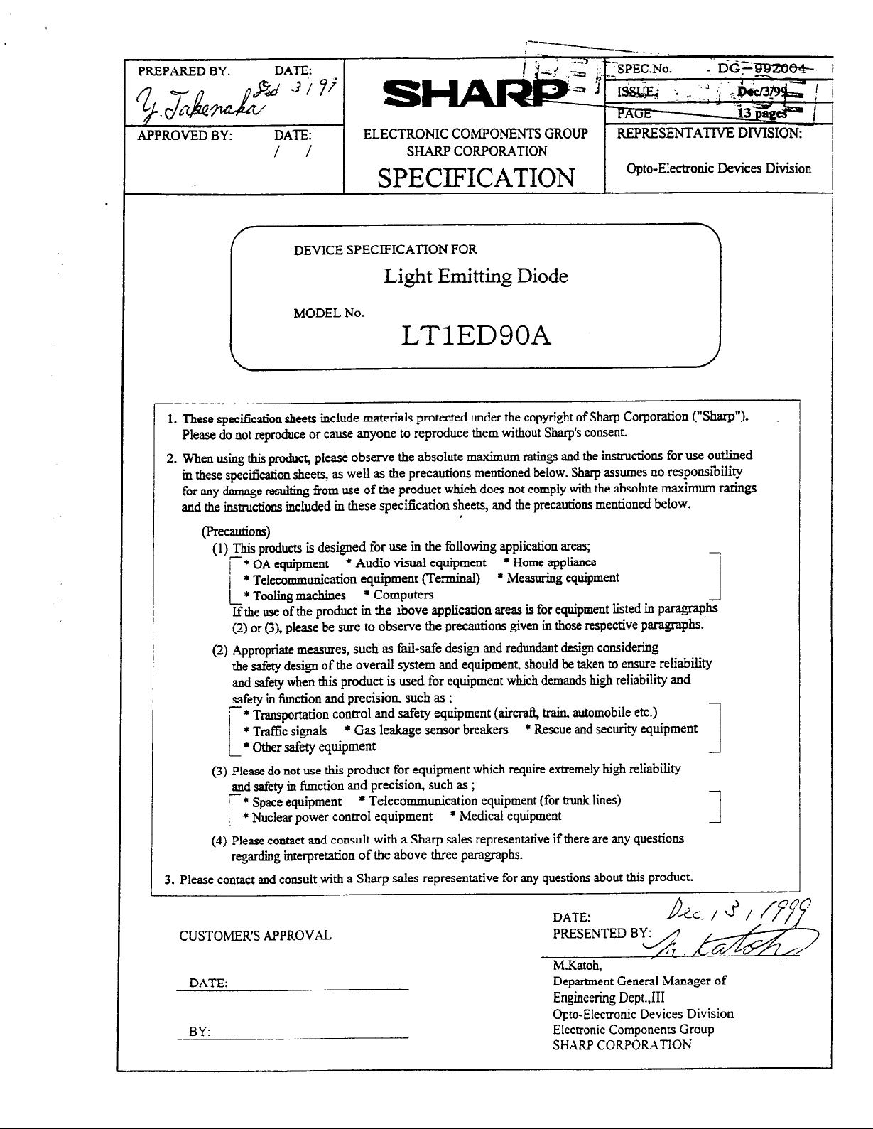
PREPARED BY: DATE:
JJ&,~ -2 ;
APPROVED BY: DATE: ELECTROMC COMPONENTS GROUP REPRESENTATIVE DMSION:
/ /
97
s-a 1 ‘I&j& .: ,,_ :-: fi -.-:
SHARP CORPORATION
-I ,.--
3
: a ;:,+;SPEC.No.
PALa
Opto-Electronic Devices Division
-_ ti~~~t34-.
SPECIFICATION
DEVICE SPECIFICATION FOR
Light Emitting Diode
MODEL No.
LTlED9OA
1. These specification sheets include materials protected under the copyright of Sharp Corporation (“Sharp”).
Please do not reproduce or cause anyone to reproduce them without Sharp’s consent.
2. When using this produ& please observe the absolute
in these specification sheets, as well as the precautions mentioned below. Sharp assumes no responsibility
for any damage resuking from use of the product which does not comply with the absolute maximum ratings
and the instructions included in these specification sheets, and the precautions mentioned below.
maximm ratings and the instructions for use outlined
(Precautions)
(1) This products is designed for use in the following application areas;
r * OA equipment * Audio visual equipment * Home appliance
* Telecommunication equipment (Terminal)
* Tooling machines
L
If the use of the product in the above application areas is for equipment listed in paragraphs
(2) or (3). please be sure to observe the precautions given in those respective paragraphs.
(2) Appropriate measures, such as W-safe design and redundant design considering
the safety design of the overall system and equipment, should be taken to ensure reliability
and safety when this product is used for equipment which demands high reliability and
safety in fimction and precision, such as ;
r * Transportation control and safety equipment (aircra& train, automobile etc.)
* Tra& signals
* Other safety equipment
1
(3) Please do not use this product for equipment which require extremely high reliability
and safety in fLnction and precision, such as ;
r * Space equipment
L * Nuclear power control equipment
(4) Please contact and consult with a Sharp sales representative if there are any questions
regarding interpretation of the above three paragraphs.
3. Please contact and consult ,tith a Sharp sales representative for any questions about this product.
CUSTOMER’S APPROVAL
DATE:
BY:
* Computers
* Gas leakage sensor breakers * Rescue and security equipment
* Telecommunication equipment (for trunk lines)
l
* Measuring equipment
Medical equipment
DATE:
PRESENTED BY.
M.Katoh,
Department General iManager of
Engineering Dept.,111
Opto-Electronic Devices Division
Electronic Components Group
SHARP CORPORXTION
AC. / J /
4 &,I
Al .
1
1
I
f7yy
Page 2
LTlEDSOA Srxcifmtion
1. Application
This specification applies to the light emitting diode device Model No. LTlEDSOA.
[GaPCienow-green)tG~/G~~ed)chip LED device]
,:‘..;
. \
2. Outline dimensions and terminal connections
3. Ratings and characteristics
. . . . . . . . . . . . . . . . . . . . . . . . . . . . . . . . . . . . . . . .
. . . . . . . . . . . ..-.........Refertothe attached sheet Page 2.
Refer to the attached sheet Page 3 -6.
3-1. Absolute maximum ratings
3-2. Electra-optical characteristics
3-3. Derating Curve
3-4. Yellow-green Characteristics Diagram
3-5. Red Characteristics Diagram
4. Reliability
. . . . . . . . . . . . . . . . . . . . . . . . . . . . . . . . . . . . . . . . . . . . . . . . . . . . . . .
4- 1. Test items and test
conditions
Refer to the attached sheet Page 7.
4-2. Failure judgement criteria
-,
,-.
1.
,.:
5. lncoeg inspection . . . . . . . . . . . . .
5- 1. Inspection method
5-2. Des-cription of inspection and criteria
6. Taping specikation
. . . . . . . . . . . . . . . . . . . . . . ..*....................*
. . . . . . . ..*.......................
Refer to the attached sheet Page 8.
Refer to the attached sheet Page 9- 11.
6-1. Taping
6-2. Packing specification
6-3. Label
6-4. Luminous intensity rank
7. Soldering.. . . . . . . . . . . . . . . . . . . . . . . . . . . . . . . . . . . . ..*................
7-1. Reflow soldering
* precautions foruse...............................................
S- 1. Precautions matters for designing circuit
8-2, Cleaning method
9. Enhamenp.. . . . . . . . .
*.........................................
9- 1. Ozonosphere destructive chemicals.
9-2. Bromic non-burning materials
>Refer to the attached sheet Page 12.
Refer to the attached sheet Page 13.
Refer to thy attached sheet Page 13.
Page 3
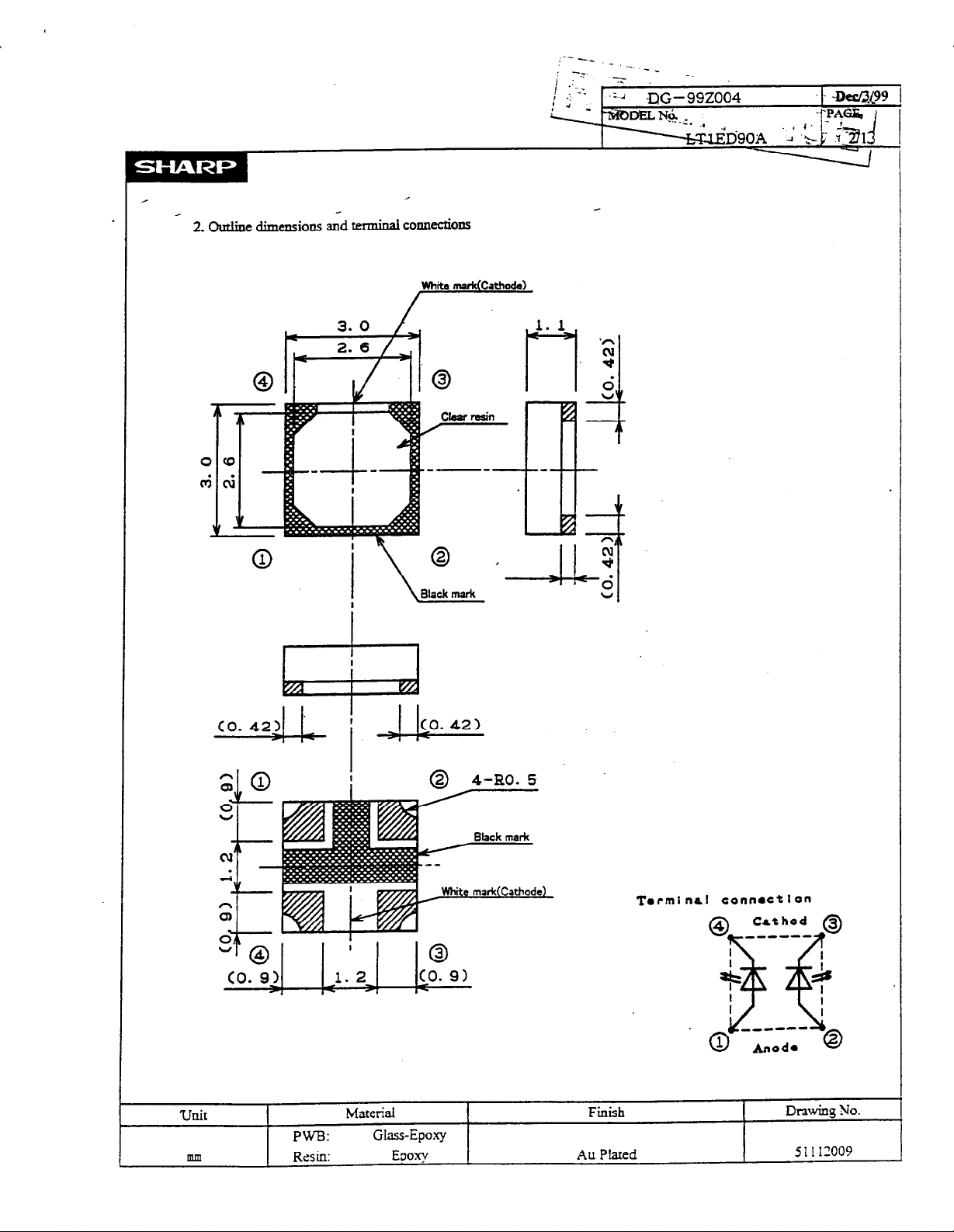
2. outline dimensions and terminal c~~ecfio~
Material Finish
PWB:
Glass-Epoxy
Resin: Epoxy
Au Plated
Torminrl
connoctlon
4
Drawing No.
51112009
Page 4
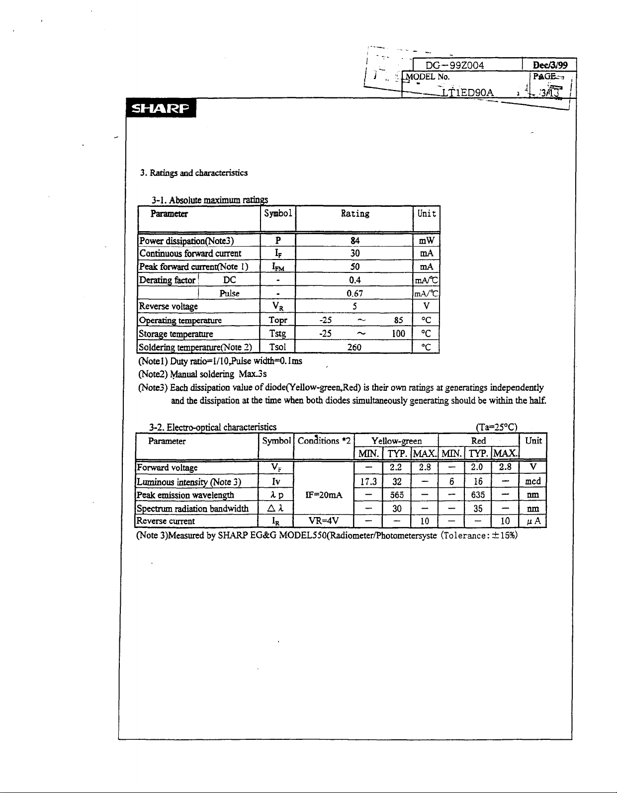
3. Ratings aad characteristics
(Notel) Duty ratio=I/1O,Pulse width=O.Ims
(Note2) &lamal soldering Max&
(Note3) Each dissipation value of diode(Yellow-green,Red) is their own ratings ar generatings independently
and the dissipation at the time when both diodes simultaneously generating should be within the half.
(Note 3)Measure.d by SHARP EG&G MODEL550(Radiometer/Photometersyste (Tolerance : t 15%)
,
Red unit
MIN. 1 I-YIP. IMAX.
-
I 2.0 I 2.8 I v
Page 5
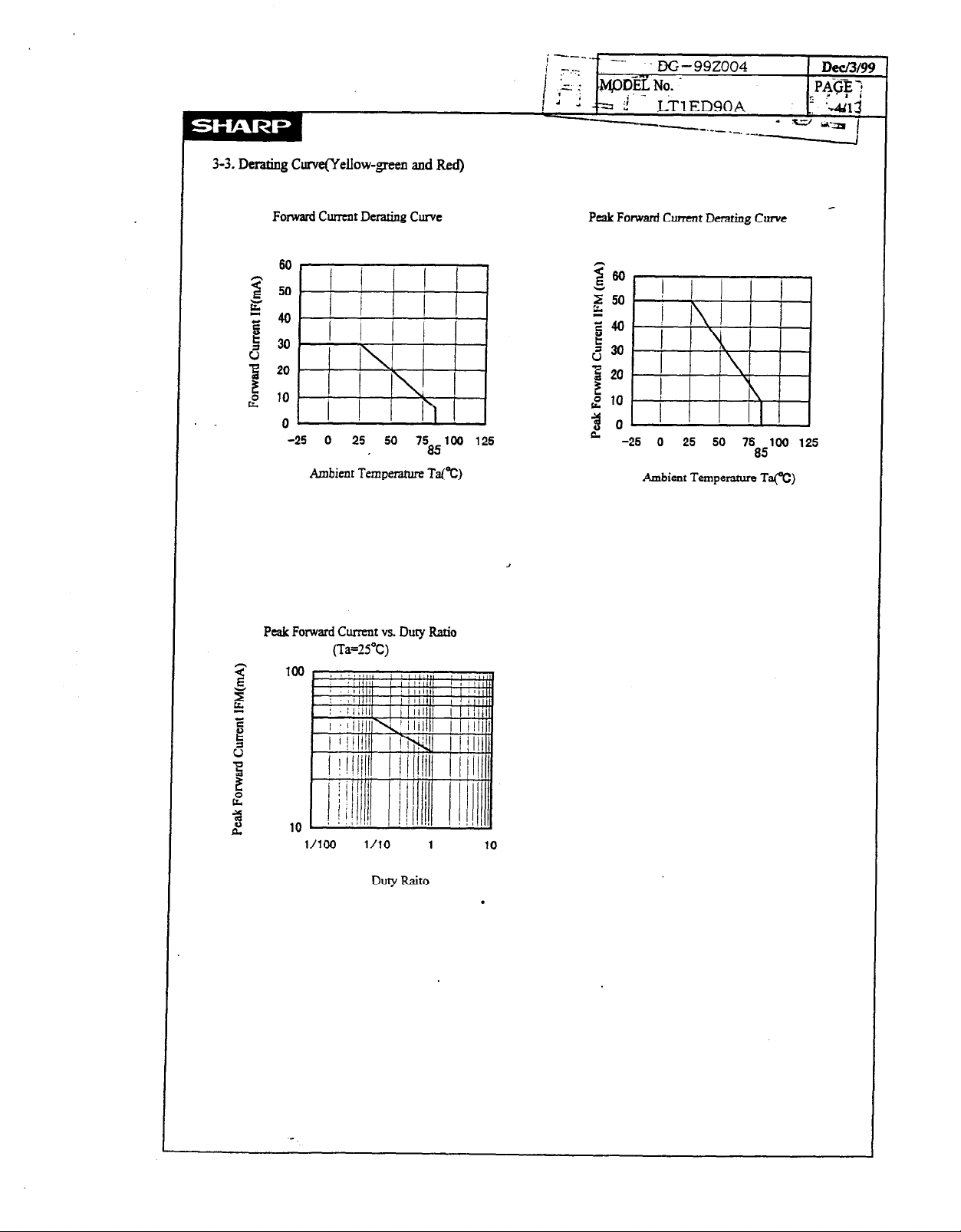
3-3. D&g Curve(Yellow-green and Red)
i ---.- -.__
DG-992004
* --._____
D&3/99
Fotward Current Denting Curve
-25 0
25 50 7585100 125 0 25 50 75g5100 125
Ambient Temperature Ta(“c)
Peak Forward Current vs. Duty Ratio
(Ta=25”C)
PeakForward
CurentDemtingCurve
Ambient Temperature Tfl)
DuryRAo
.
Page 6

34.
Yellow-green Chamcteristi~~ Diagram(typ) (Note 1)
-- -.-____
‘y--. -. r
%-
-.-_-_ _ _
D6- 992004
.LTlEDSOA .
---- --
*- *> - ’
Deem99
.
0. 1
Fomard Current vs.Fomard Volee
1
1.2
1.4 1.6
1.8 2 2.2 2.4
Forward Voltage VF(v)
(Ta=25"C)
Relative Luminous Intensity
vs. Ambient Tap-
1000
g
2
z
2
2 100
B
.-
E
3
:
.9
d 10
-60 -40 -20 0 20 40 60 80
Ambient Temprat~~~~
m=2omw
100 120
Ta(“C)
0. 1
(Note 1) Above
I / iii/iii/ i
1
Forward Current IF(mA)
characteristic data are typical data and not a ,guaran
10 100
tteed data.
Page 7

3-5. Red Chamctetistics Diagam(typ) (Note 1)
DG-992004
D&/99
Forward Current vnForward Voltage
100
0. 1
1 1.2 1.4 1.6 1.8 2 2.2 2.4
Forward Voltage VF(v)
Relative Luminous Intensity
vs. Ambient Temperature
aF=2omA~
1000
c
b
z
B
Y
5 100
a
.B
E
3
0
.z
P
2 10
-60 -40 -20 0 20 40
l
Ambient
Tmpraxure Ta(“cI
60 80 100 120
0. 1
(Note
1) Above characteristic data are
1
Forward CummtE=(mA)
10 100
typical data
and not a gmantteed dam
Page 8

4.
Reliability
The reliability of products shall be satisfied with items listed below.
r
4-l. Test items and test
conditions
Test items
temperature cycling
High temp. andhigh
humidity storage
figh mpe&ure storage
E
.ow
temperature
I
Operating test
Mechanical shock
Variable titquency
ViilY3tiOil
Soldering heat
-25”c(3Omin)-+lOO”c(3Omin),3Otimes
Ta=+60”C, 9O%RH, HOOh
Ta= 1 OO”C,t+OOh
storage Ta=25”C,t=SOOh
Ta=25”C,1,=30mA,r500h
15 ooom/s’, osms,
3times / kX$Y,*Z direction
2OOm/s*, 100-2 OOO-lOOHz/sweepfor 4min.
,4timeaYz direction
Refer to the attached sheq
Page 1 l/12 ltimes
4-2. Failure ju&ement criteria * 1
Parameter
Symbol Failure judgement criteria *2
Test conditions
,
Cotidence level: 90%
Samples (Il) LTPD
Defective (C) (%)
n=32, c=o
n-22, c=o
10
10
n=22, c=o 10
n=“, c=o 10
n=22, Go 10
n=ll, C=O 20
n=ll, C=O 20
n=ll, c=O 20
Forward voltage
Reverse current
Luminous intensity
vF
IR
IV
Iv > The first stage value X 2.0 or The tit stage value X 0.5 > Iv
* 1: Measuring condition is in accordance with specification.
*2: U.S.L. is shown by Upper Specification Limit.
v, > U.S.L. x 1.2
Ia > U.S.L. x 2.0
Page 9

5. Incoming inspection .-
5- 1. Inspection method
A single sampling plan, normal inspection level S-4 based on IS0 2859-l shah be adopted
J-L. u~b,Ipu”l.l “I uqJ’.*LA”Y LIYY VA-.--
FIO.
Inspection items
Criteria
Defect
A@
1
Electra-optical
Charactenstlcs
. .
2 Radiation color
3
4
5
6
7
Taping
Label
Solderbility 1
Electra-optical
Characteristics
Outline dimensions
8
Not radiation
Not correct
Product inserted in reverse direction
Model number is not printed,or misprinted
Plating abnormality observed over 50% or
greater percentage * 1
Not conforming to the specification
Not conforming to the specification
Dust
: @ 0.8nun or more
Thread dust : 2.5mm or more in length and 0.25mm or
more in width
Air bubbles : 4 0.8mm or more
Scratch : 2.5n.u.n or more in length and 025mm or more in
width
However&e product is qualified as a good unit if the
-scrach does not touch the Auwire.when seen from the front.
Resin batr : Effect to the specification
Major
defect
I’
Minor
defect
0.1%
0.4%
9 Solderbility 2
Judgement area
The
Resin flash:Over the unspecified tolerance
Resin ond plated crack :0.3mm or more
could solder 50% or greater and less than 90% out of
judgement area * 1
plated area of the product bottom
Page 10

6.Taping specificarion
6-l.Taping
6-1-l.Shape and dime&on of tape(lYF’.)
_. __ _
: I--
i :‘--
DG- 992004
MODELNo. -
: .a LTlEDSOA - 5 &I?
_ 2’
.& &
-------Ad
De&/99
P&G<
‘:-.a
6-l-2.Shape and dimension of reel(TYP.)
Page 11

6-l-3 .Taping specification
(1) Lead tape:
DG-992004
MbDEL No.
Deem99
PAGE
z LTlEDSOA ’ -IQ8443
j 3
4 - .I
--- ‘.
Pull ,,,I--> __
.
End
000000
0000000000
q ICIU~ q mnn 170
Empty -I- Stuffed A-
(2) Cover tape strength against peeling:P=O.l-O8N( 0 =lO’or less)
Cover tape
c ’ - ‘yape speed : Smm/s
<- Forward
Carrier tape
(3) Tape strength against bending:
The radius of bending circle should be 3Omm or more.
Ifit is less than 3Omm, the cover may peel.
(4) Jointing of tape:
(5) Quantity per reel:
(6) Mass per products:
(7)Mass per packing:
(8) Others:
@ There should not be missing above continuous three products.
There should not be joint of cover tape or carrier tape.
Average 3,OOOpcs. per reel
Average 0.02g 1 product
Average 150g I packing
@ Products should be easily taken out
@ Products should not be attached to the cover tape at peeling.
6-2. Packing specification
6-2- 1. Dampproof package
In other to avoid the absorption of humidity in transport and storage,
in aluminum sleeve.
Empty
’ 10 pitch or ‘more
Begirming
I-Leading
40-50 pitch
the device s are packed
Lab.31
6-2-2.Strage conditions
Temperature : 5
to 30°C
Humidity : less than 6O%RH
6-2-3.Trement after opening
(1) Please make a soldering within 15 days after opening under following condition;
Temperature : 5 to 30°C Humidity : less than 6O%RH
(2) In case the devices are not used for a long tune after opening ,the storage in dry box is recommendable.
Or it is better to repack the devices with a desiccative by the sealer and put them in the some storage
conditions
as 6-2-2. Then they should be used within 2 weeks.
(3) Please make a soldering after a follewing baking treatment if unused term should be over the conditions of (2)
*Recommendable conditions:
0 in taping
Temprature:6O’C to 6Y’C,Time:j6 to 38 hours
0 in individual (on PWB or metallic tray)
Tempnture: IOO’C to 13Oc .Time:Z to 3 hours
Page 12

6-3.
Label _
+ Model number
- Qmtity of products
+-EIkTG3Barcode
I
LOT No.KA99B19 RANK O-0
<EIAJ C-3> WE IN JAPAN
+ EL4J C-3 Bar code
+ Lot number l and Luminous rank, dominant wavelength rank
+ Reduction country
@ Prodwtion plant code@0 be indicated alphabetically)
@ Roduetion lot(single or double figures)
@ Year of production(tbe last two figures of the year)
. @ Month of production
(to be indicated alphabetically with January corresponding to A)
@ Date of production(0 l-3 1)
1
6-4.Luninous intensity rank(Note 1)
(Yeiiow-green)
.
B 173 -
C 25.0 -
D
Luminous intensity unit condition
33.8
36.0 -
48.8
(70.2)
mcd
(Ta=25”C)
I&!OmA
(Tolerance : + 15%)
CRe4
.
A
B
C
D
Dominant wavelength Unit Condition
6.0 -
8.8 -
12.7 -
18.3 -
11.8
17.0
24.6 Ml
(35.5)
(Ta=25”C)
IpZOmA
(Tolerance: F 15%)
(Note 1)
Also I shaIl not ask the delivery ratio of each rank.
(Note 2) This rank value is the setting value of when that classifies it the rank and be not a guarantee value.
Page 13

-- -my
;-..
z-*, a_
J J
-‘Q ,y *
MODEL No.
i’- *> *-
,-.>
.7; .
-
: .--
i .,--.
I
----__c:. .
7. Soldering
7; 1 .Reflow soldering
(1) It is not recommended to exceed the soldering temperature and time shown below.
Caused by substrate bend or the other mechanical stress during reflow soldering
may happen gold wire disconnection etc. Therefore please check and study your
solder reflow machine’s best condition.
(2) Reflow soldering temperature profile
to be done under the following condition.
140-160
- 992004
DG
-LTIEDSOA
-.- -. .___
1 DedY99
PAGE
_
--.-.
.,-> ‘2X4 :
l2/13
g
Time(s)
Recommendable Thermal Model
(3) Recommendable Metal ~Mask pattern for screen print
Recommend 0.3m.m to 0.5~1 thickness metal mask
for screen print Caused by solder reflow $ondition,
solder
paste,
substrate and the other material etc.,
may change solderbility.
Please check and study actual solderbility before
usage.
*Center of the moduct
1 1.2 1 llO/
1.24
r- -r-
-
Recommended soldar pattern
(Unir:mxn)
Page 14

i--.._
i ‘.--.’
J.= J ,v+““--
i 4 y= i-,J T;TlEDgOi
i
i
_ DG- 992004
L L:i ~
- . . _. :
.
8. Recautions for use
8- 1. &cautions matters for designing circuit
This product is not designed as electromagnetic and ionized-particle radiation resistant
8-2. Cleaning method
Use only the following types of solvent.%ater”
Recommend conditions: RT. 4OkHz, 3OW/l, time is more than 3 minutes
The alkt on the device f?om ultrasonic bath, ultrasonic output, duration, board size and device mounting method.
Test the cleaning method under actual conditions and check for abnormalities before actual use.
9. Environment
9- 1. Ozonosphere destructive chemicals.
(1) The device doesn’t contain following substance.
(2) The device doesn’t have a production line whose process requires following substance.
Restricted part: CFCs,halones,CC~,Trichloroetbane(Methychloroform)
1 Dee/3/99
9-2. Bromic non-bum& materials
I
The device doesn’t contain bromic non-burning materials(PBBOs,PBBs)
.
Page 15

LT1ED90A
 Loading...