

Page 1
LT1675/LT1675-1
250MHz, Triple and Single
RGB Multiplexer with Current Feedback Amplifiers
FEATURES
■
100MHz Pixel Switching
■
– 3dB Bandwidth: 250MHz
■
Small 16-Pin SSOP Package
■
Channel Switching Time: 2.5ns
■
Expandable to Larger Arrays
■
Drives Cables Directly
■
High Slew Rate: 1100V/µs
■
Low Switching Transient: 50mV
■
Shutdown Supply Current: 0mA
■
Output Short-Circuit Protected
U
APPLICATIONS
■
RGB Switching
■
Workstation Graphics
■
Pixel Switching
■
Coaxial Cable Drivers
■
High Speed Signal Processing
U
DESCRIPTION
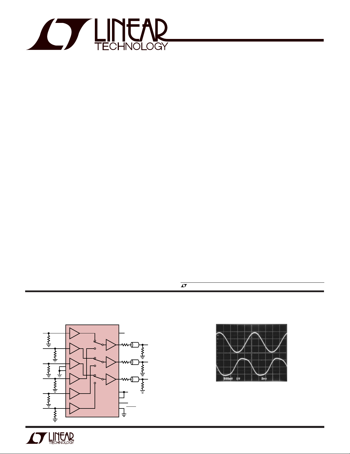
The LT®1675 is a high speed RGB multiplexer designed for
pixel switching and fast workstation graphics.
Included on chip are three SPDT switches and three
current feedback amplifiers. The current feedback amplifiers drive double-terminated 50Ω or 75Ω cables and are
configured for a fixed gain of 2, eliminating six external
gain setting resistors. The SPDT switches are designed to
be break-before-make to minimize unwanted signals coupling to the input.
The LT1675-1 is a single version with two inputs, a single
output and is ideal for a single channel application such as
video sync.
The key to the LT1675 fast switching speed is Linear
Technology’s proprietary high speed bipolar process. This
MUX can toggle between sources in excess of 100MHz,
has a slew rate over 1000V/µs and has a –3dB bandwidth
of 250MHz. The speed and ease of use of the LT1675 make
it ideal for high performance PCs, workstations and professional video monitors. The input-referred switching
transient is only 50mV
and lasts just 5ns, making it
P-P
virtually undetectable. Power supply requirements are
±4V to ±6V and power dissipation is only 300mW on ±5V,
or 100mW for the LT1675-1. The expandable feature uses
the disable pin to reduce the power dissipation to near
0mW in the off parts.
Unlike competitive solutions that are in bulky high pin
count packages, the LT1675 is in a 16-lead narrow body
SSOP. This small footprint, the size of an SO-8, results in
a very clean high performance solution. The LT1675-1 is
available in the tiny MSOP and the SO-8.
, LTC and LT are registered trademarks of Linear Technology Corporation.
TYPICAL APPLICATION
High Speed RGB MUX
RED 1
75Ω
GREEN 1
75Ω
BLUE 1
75Ω
RED 2
75Ω
GREEN 2
75Ω
BLUE 2
75Ω
LT1675
+1
+1
+1
+1
+1
+1
+2
+2
+2
U
75Ω
75Ω
75Ω
+
V
ENABLE
CABLE
CABLE
CABLE
–
V
SELECT RGB1/RGB2
V
75Ω
V
75Ω
V
75Ω
OUT RED
OUT GREEN
OUT BLUE
1675 TA01
Select Pin Switches Inputs at 100MHz
3V
SELECT
LOGIC
PIN 10
0V
1V
RED
OUT
0V
RED 1 = 0V, RED 2 = 1V, RL = 100Ω
MEASURED BETWEEN 50Ω BACK TERMINATION AND 50Ω LOAD
1V/DIV
500mV/DIV
1675 TA02
1
Page 2
LT1675/LT1675-1
WW
W
ABSOLUTE MAXIMUM RATINGS
U
(Note 1)
Supply Voltage ..................................................... ±6.3V
Inputs, ENABLE and SELECT, Current ................ ±20mA
Output Short-Circuit Duration (Note 2).........Continuous
Specified Temperature Range (Note 3)....... 0°C to 70°C
U
W
U
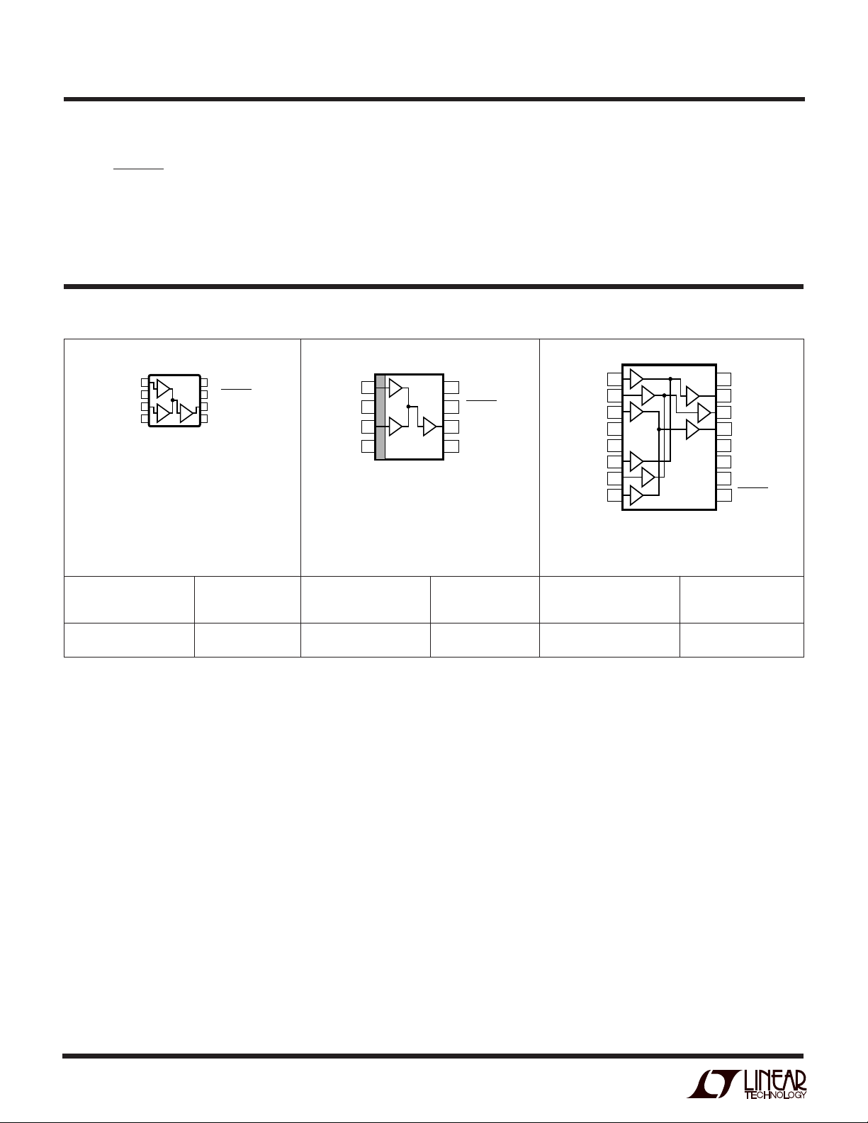
PACKAGE/ORDER INFORMATION
TOP VIEW
V
1
IN1
2
GND
3
V
IN2
–
4
V
MS8 PACKAGE
8-LEAD PLASTIC MSOP
T
= 150°C, θJA = 250°C/ W
JMAX
8
V
7
ENABLE
6
V
5
SELECT
+
OUT
V
IN1
GND
V
IN2
V
TOP VIEW
1
2
3
–
4
S8 PACKAGE
8-LEAD PLASTIC SO
T
= 150°C, θJA = 150°C/ W
JMAX
Operating Temperature Range ................ –40°C to 85°C
Storage Temperature Range ................. –65°C to 150°C
Junction Temperature (Note 4)............................ 150°C
Lead Temperature (Soldering, 10 sec).................. 300°C
TOP VIEW
8
7
6
5
+
V
ENABLE
V
OUT
SELECT
1
RED 1
GREEN 1
GREEN 2
2
3
BLUE 1
4
GND
5
GND
6
RED 2
7
8
BLUE 2
GN PACKAGE
16-LEAD PLASTIC SSOP NARROW
T
= 150°C, θJA = 120°C/W
JMAX
16
15
14
13
12
11
10
9
+
V
V
OUT RED
V
OUT GREEN
V
OUT BLUE
–
V
–
V
SELECT
ENABLE
ORDER PART
NUMBER
LT1675CMS8-1
MS8 PART
MARKING
LTGX
Consult factory for Industrial and Military grade parts.
ORDER PART
NUMBER
LT1675CS8-1
S8 PART
MARKING
16751
ORDER PART
NUMBER
LT1675CGN
GN PART
MARKING
1675
2
Page 3
LT1675/LT1675-1
ELECTRICAL CHARACTERISTICS
0°C ≤ TA ≤ 70°C, VS = ±5V, RL = ∞
= 0V LT1675 (Pins 1, 2, 3, 6, 7, 8),
, VIN
LT1675-1 (Pins 1, 3), ENABLE = 0V, unless otherwise specified.
PARAMETER CONDITIONS MIN TYP MAX UNITS
Output Offset Voltage Any Input Selected ● 20 40 mV
Output Offset Matching Between Outputs R1 to R2, G1 to G2, B1 to B2 ● 520 mV
Input Current Any Input Selected ● –12 –30 µA
Input Resistance VIN = ±1V ● 100 700 kΩ
PSRR VS =±2.6V to ±6V, Measured at Output ● 38 50 dB
DC Gain Error 0V to 1V VIN = 1V, R
V
= 1V, RL = 150Ω ● 48 %
IN
= 1V, RL = 75Ω ● 510 %
V
IN
DC Gain Error 0V to –1V VIN = –1V, R
= –1V, RL = 150Ω ● 48 %
V
IN
V
= –1V, RL = 75Ω ● 820 %
IN
Output Voltage VIN = 2V, R
V
= 2V, RL = 150Ω ● 2.8 3.0 V
IN
= 2V, RL = 75Ω ● 2.4 2.8 V
V
IN
VIN = –2V, R
= –2V, RL = 150Ω ● –2.7 – 3.0 V
V
IN
V
= –2V, RL = 75Ω ● – 2.3 – 2.6 V
IN
Disabled Output Impedance ENABLE Open ● 1.1 1.5 2.0 kΩ
Maximum Output Current VIN = ±1V, VO = 0V ● 50 70 mA
Supply Current LT1675 ENABLE = 0V ● 25 33 42 mA
ENABLE = 4.7V
LT1675-1 ENABLE = 0V ● 81114 mA
ENABLE = 4.7V
ENABLE Pin Current LT1675 ENABLE= 0V ● 450 600 µA
LT1675-1 ENABLE= 0V ● 150 200 µA
SELECT Pin Current LT1675 SELECT = 0V ● 90 180 µA
LT1675-1 SELECT = 0V ● 30 60 µA
SELECT Low SELECT (See Truth Table) ● 0.8 V
SELECT High SELECT (See Truth Table) ● 2V
= ∞ ● 36 %
L
= ∞ ● 36 %
L
= ∞ ● 3.1 3.4 V
L
= ∞ ● –3.1 –3.3 V
L
● 1 100 µA
● 0.3 33 µA
3
Page 4

LT1675/LT1675-1
AC CHARACTERISTICS
0°C ≤ TA ≤ 70°C, VS = ±5V, RL = 150Ω
= 0V LT1675 (Pins 1, 2, 3, 6, 7, 8),
, VIN
LT1675-1 (Pins 1, 3), ENABLE = 0V, unless otherwise specified.
PARAMETER CONDITIONS MIN TYP MAX UNITS
Slew Rate V
Full Power Bandwidth (Note 5) V
Small-Signal –3dB Bandwidth Less Than 1dB Peaking 250 MHz
Gain Flatness Less Than 0.1dB 70 MHz
Gain Matching R to G to B 0.10 dB
Channel-to-Channel Select Time R1 = 0V, R2 = 1V
Delay Time Measured from Time SELECT Pin Crosses Logic Threshold 5.0 ns
Switching Time Time for V
Enable Time 10 ns
Disable Time 100 ns
Input Pin Capacitance 2pF
SELECT Pin Capacitance LT1675 2.2 pF
LT1675-1 1.5 pF
ENABLE Pin Capacitance LT1675 2.1 pF
LT1675-1 1.5 pF
Output Pin Capacitance (Disabled) ENABLE Open 4.4 pF
Small-Signal Rise Time VIN = 300mV
Propagation Delay VIN = 300mV
Overshoot VIN = 300mV
On-Channel to Off-Channel Crosstalk Measured at 10MHz 60 dB
Chip Disable Crosstalk Measured at 10MHz, ENABLE Open 90 dB
Channel Select Output Transient Measured Between Back Termination and Load 50 mV
Differential Gain (Note 6) 0.07 %
Differential Phase (Note 6) 0.05 DEG
= 5V
OUT
P-P
=6V
OUT
P-P
R1 to R2, G1 to G2, B1 to B2, LT1675-1 V
to Go from 0V to 1V 2.5 ns
OUT
, RL = 100Ω 1.85 ns
P-P
, RL = 100Ω 3ns
P-P
, RL = 100Ω 10 %
P-P
IN1
to V
IN2
1100 V/µs
58 MHz
0.01 dB
P-P
The
● denotes specifications that apply over the specified temperature
range.
Note 1: Absolute Maximum Ratings are those values beyond which the life
of a device may be impaired.
Note 2: May require a heat sink.
Note 3: The LT1675/LT1675-1 are guaranteed to meet specified
performance from 0°C to 70°C and are designed, characterized and
expected to meet these extended temperature limits, but are not tested at
–40°C and 85°C. Guaranteed I grade parts are available; consult factory.
Truth Table
SELECT ENABLE RED OUT GREEN OUT BLUE OUT VOUT
1 0 RED 1 GREEN 1 BLUE 1 VIN1
0 0 RED 2 GREEN 2 BLUE 2 VIN2
X 1 OFF OFF OFF OFF
4
Note 4: TJ is calculated from the ambient temperature TA and power
dissipation P
LT1675CGN: T
LT1675CMS8-1: T
LT1675CS8-1: T
Note 5: Full power bandwidth is calculated from the slew rate
measurement:
FPBW = SR/2πV
Note 6: Differential Gain and Phase are measured using a Tektronix
TSG120 YC/NTSC signal generator and a Tektronix 1780R Video
Measurement Set. The resolution of this equipment is 0.1% and 0.1°. Nine
identical MUXs were cascaded giving an effective resolution of 0.011%
and 0.011°.
LT1675 LT1675-1
according to the following formula:
D
= TA + (PD)(120°C/W)
J
= TA + (PD)(250°C/W)
J
= TA + (PD)(150°C/W)
J
.
PEAK
Page 5
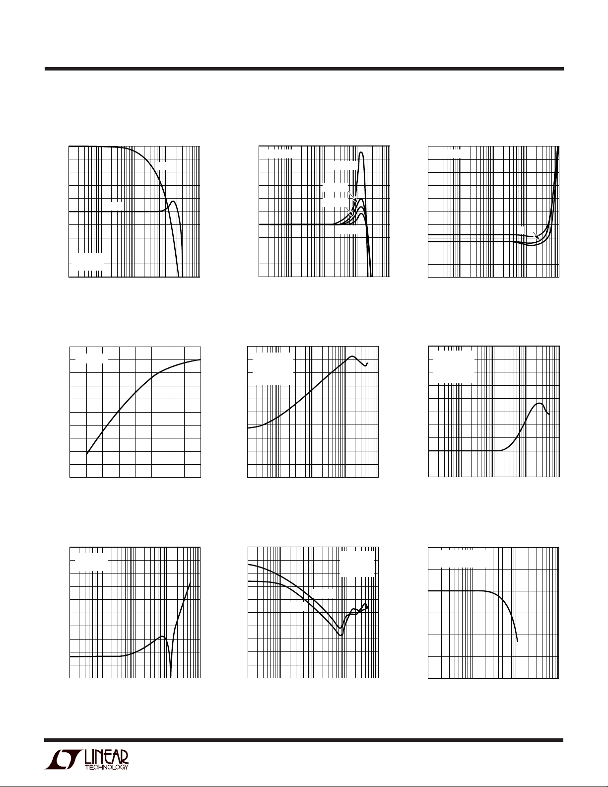
UW
TYPICAL PERFORMANCE CHARACTERISTICS
LT1675/LT1675-1
Gain and Phase vs
Frequency
5
4
3
2
1
0
GAIN (dB)
–1
–2
–3
CL = 0pF
–4
R
L
–5
100k 10M 100M 1G
GAIN
= 150Ω
1M
FREQUENCY (Hz)
PHASE
–3dB Bandwidth vs
Supply Voltage
300
RL = 150Ω
280
260
240
220
200
180
FREQUENCY (MHz)
160
140
120
100
2
3
SUPPLY VOLTAGE (±V)
4
5
1675 G01
1675 G04
0
–20
–40
–60
PHASE (DEG)
–80
–100
–120
–140
–160
–180
–200
GAIN (dB)
Crosstalk Rejection vs Frequency
–30
–40
–50
–60
–70
–80
–90
–100
CROSSTALK REJECTION (dB)
–110
–120
–130
6
100k 10M 100M 1G
Frequency Response with
Capacitive Loads
6
RL = 150Ω
5
4
3
2
1
0
–1
–2
–3
–4
100k 10M 100M 1G
RS = 75Ω
R
R1 DRIVEN
R2 SELECTED
= 150Ω
L
1M
1M
FREQUENCY (Hz)
CL = 10pF
CL = 5pF
CL = 3pF
CL = 0pF
FREQUENCY (Hz)
1675 G02
1675 G05
Gain vs Frequency
6.5
RL = 100Ω
6.4
6.3
6.2
6.1
6.0
GAIN (dB)
5.9
5.8
5.7
5.6
5.5
10k 1M 10M 100M
100k
FREQUENCY (Hz)
R
Crosstalk Rejection vs Frequency
20
RS = 75Ω
10
= 150Ω
R
L
G1 DRIVEN
0
R1 SELECTED
–10
–20
–30
–40
–50
CROSSTALK REJECTION (dB)
–60
–70
–80
100k 10M 100M 1G
1M
FREQUENCY (Hz)
G
B
1675 G03
1675 G23
Crosstalk Rejection vs Frequency
(Disabled)
–10
RS = 75Ω
–20
= 150Ω
R
L
–30
–40
–50
–60
–70
–80
CROSSTALK REJECTION (dB)
–90
–100
–110
100k 10M 100M 1G
1M
FREQUENCY (Hz)
1675 G06
Power Supply Rejection Ratio
vs Frequency
70
60
50
40
30
20
10
0
–10
–20
POWER SUPPLY REJECTION RATIO (dB)
–30
100k 10M 100M 1G
–PSRR
1M
FREQUENCY (Hz)
+PSRR
VS = ±5V
= 25°C
T
A
= 150Ω
R
L
1675 G07
Undistorted Output Swing
vs Frequency
8
VS = ±5V
= 150Ω
R
L
7
)
P-P
6
5
4
OUTPUT VOLTAGE (V
3
2
1M
10M 100M 1G
FREQUENCY (Hz)
1675 G08
5
Page 6

LT1675/LT1675-1
W
U
TYPICAL PERFORMANCE CHARACTERISTICS
Output Impedance vs Frequency
10k
DISABLED
1k
100
10
OUTPUT IMPEDANCE (Ω)
ENABLED
1
100k 10M 100M 1G
1M
FREQUENCY (Hz)
Output Short-Circuit Current
vs Temperature
90
VS = ±5V
85
80
75
70
65
60
55
OUTPUT SHORT-CIRCUIT CURRENT (mA)
50
–50
050
–25 25 75 125
TEMPERATURE (°C)
SOURCING
V
IN
SINKING
= –1V
V
IN
= 1V
100
1675 G09
1675 G13
2nd and 3rd Harmonic Distortion
vs Frequency
–30
RL = 150Ω
= 2V
V
O
–40
–50
–60
DISTORTION (dBc)
–70
–80
1
P-P
2ND
3RD
10 100
FREQUENCY (MHz)
Positive DC Gain Error vs
Temperature
4
VS = ±5V
= 1V
V
IN
3
2
GAIN ERROR (%)
1
0
–25 25 75 125
–50
RL = 75Ω
RL = 150Ω
050
TEMPERATURE (°C)
LTXXXX 1675 G10
100
1675 G14
Input Bias Current vs
Input Voltage
15
VS = ±5V
10
5
0
–5
–10
–15
INPUT BIAS CURRENT (µA)
–20
–25
–30
–3 –2 0 2
INPUT VOLTAGE (V)
125°C
–1 3
Negative DC Gain Error vs
Temperature
12
VS = ±5V
= –1V
V
IN
10
8
6
GAIN ERROR (%)
4
2
0
–50
RL = 75Ω
RL = 150Ω
–25 0
50 100 125
25 75
TEMPERATURE (°C)
–55°C
25°C
1
1675 G12
1675 G15
Output Voltage vs Input Voltage
4
VS = ±5V
3
T
= 25°C
A
2
1
0
–1
OUTPUT VOLTAGE (V)
–2
–3
–4
–2
–1
INPUT VOLTAGE (V)
RL = 75Ω
0
6
RL =
1
∞
RL = 150Ω
2
1675 G16
Supply Current vs Supply Voltage
40
RL =
35
30
25
20
15
SUPPLY CURRENT (mA)
10
∞
5
0
01
125°C
243
SUPPLY VOLTAGE (±V)
25°C
–55°C
5
1675 G11
LT1675-1 Supply Current vs
Supply Voltage
14
RL =
∞
12
10
8
6
4
SUPPLY CURRENT (mA)
2
6
0
01
SUPPLY VOLTAGE (±V)
243
125°C
25°C
–55°C
5
6
1675 G24
Page 7

W
U
TYPICAL PERFORMANCE CHARACTERISTICS
LT1675/LT1675-1
INPUT BIAS CURRENT (µA)
SELECT
PIN 10
RED OUT
PIN 15
Input Bias Current vs
Temperature
–10
VS = ±5V
= 0V
V
IN
–11
–12
–13
–50
–25 0
25 75
TEMPERATURE (°C)
Toggling RED 2 to RED 1
3V
0V
50 100 125
1675 G17
1V/DIV
1V/DIV
Output Offset Voltage vs
Temperature
20
VS = ±5V
15
10
5
OUTPUT OFFSET VOLTAGE (mV)
0
–50 25 75
–25 0
TEMPERATURE (°C)
Slew Rate
RED 1 IN
RED OUT
PIN 15
50 100 125
1675 G18
1V/DIV
2V/DIV
RED 1 = 0V
RED 2 = UNCORRELATED SINEWAVE
= 150Ω, 10pF SCOPE PROBE 1675 G19
R
L
Small-Signal Rise Time
V
GEN
V
OUT
0V
RL = 100Ω
MEASURED WITH FET PROBES
1675 G21
50mV/DIV
50mV/DIV
ENABLE
PIN 9
RED OUT
PIN 15
MEASURED AT PIN 15
R
= 150Ω, 10pF SCOPE PROBE
L
SR = 1100V/µs
Enable and Disable
5V
0V
0V
ENABLE AND DISABLE OF UNCORRELATED
SINEWAVE
= 150Ω 1675 G22
R
L
1675 G20
2V/DIV
2V/DIV
7
Page 8

LT1675/LT1675-1
UUU
PIN FUNCTIONS
LT1675
RED 1 (Pin 1): Red 1 Input. The 1V video input signal to be
switched is applied to this pin. If 2V are applied to this pin,
V
OUT RED
will clip. The input must be terminated.
GREEN 1 (Pin 2): Green 1 Input. The 1V video input signal
to be switched is applied to this pin. If 2V are applied to this
pin, V
OUT GREEN
will clip. The input must be terminated.
BLUE 1 (Pin 3): Blue 1 Input. The 1V video input signal to
be switched is applied to this pin. If 2V are applied to this
pin, V
OUT BLUE
will clip. The input must be terminated.
GND (Pins 4, 5): Signal Ground. Connect to ground plane.
RED 2 (Pin 6): Red 2 Input. The 1V video input signal to be
switched is applied to this pin. If 2V are applied to this pin,
V
OUT RED
will clip. The input must be terminated.
GREEN 2 (Pin 7): Green 2 Input. The 1V video input signal
to be switched is applied to this pin. If 2V are applied to this
pin, V
OUT GREEN
will clip. The input must be terminated.
BLUE 2 (Pin 8): Blue 2 Input. The 1V video input signal to
be switched is applied to this pin. If 2V are applied to this
pin, V
OUT BLUE
will clip. The input must be terminated.
ENABLE (Pin 9): Chip Enable. Ground this pin for normal
operation. Take this pin to within 300mV of V+, or open to
shut down the part. This pin is also used for router
applications. When the part is disabled, the supply current
is 1µA.
SELECT (Pin 10): Channel Select. Use this pin to select
between RGB1 inputs and RGB2 inputs. Use this pin for
fast toggling. HIGH Selects RGB1.
V– (Pins 11, 12): Negative Power Supply. Connect these
pins to –5V and bypass with good tantalum capacitor
(4.7µF). The pin may also require a 0.1µF or 0.01µF
depending on layout.
V
OUT BLUE
2 depending on which channel is selected by Pin 10. V
BLUE
(Pin 13): Blue Output. It is twice BLUE 1 or BLUE
OUT
drives 50Ω or 75Ω double-terminated cables. Do not
add capacitance to this pin.
V
OUT GREEN
(Pin 14): Green Output. It is twice GREEN 1 or
GREEN 2 depending on which channel is selected by Pin
10. V
OUT GREEN
drives 50Ω or 75Ω double-terminated
cables. Do not add capacitance to this pin.
V
OUT RED
depending on which channel is selected by Pin 10. V
RED
(Pin 15): Red Output. It is twice RED 1 or RED 2
OUT
drives 50Ω or 75Ω double-terminated cables. Do not
add capacitance to this pin.
V+ (Pin 16): Positive Power Supply. Connect this pin to 5V
and bypass with good tantalum capacitor (4.7µF). The pin
may also require a 0.1µF or 0.01µF depending on layout.
LT1675-1
V
(Pin 1): The 1V video input signal to be switched is
IN1
applied to this pin. If 2V are applied to this pin, V
OUT
will
clip. The input must be terminated.
GND (Pin 2): Signal Ground. Connect to ground plane.
V
(Pin 3): The 1V video input signal to be switched is
IN2
applied to this pin. If 2V are applied to this pin, V
OUT
will
clip. The input must be terminated.
V– (Pin 4): Connect this pin to –5V and bypass with good
tantalum capacitor (4.7µF). The pin may also require a
0.1µF or 0.01µF depending on layout.
SELECT (Pin 5): Use this pin to select V
pin for fast toggling. HIGH Selects V
IN1
IN1
.
or V
. Use this
IN2
8
V
(Pin 6): It is twice V
OUT
channel is selected by Pin 5. V
IN1
or V
depending on which
IN2
drives 50Ω or 75Ω
OUT
double-terminated cables. Do not add capacitance to this
pin.
ENABLE (Pin 7): Ground this pin for normal operation.
Take this pin to within 300mV of V+, or open to shut down
the part. This pin is also used for router applications. When
the part is disabled, the supply current is 0.3µA.
V+ (Pin 8): Connect this pin to 5V and bypass with good
tantalum capacitor (4.7µF). The pin may also require a
0.1µF or 0.01µF depending on layout.
Page 9

LT1675/LT1675-1
U
WUU
APPLICATIONS INFORMATION
Power Supplies
The LT1675 will function with supply voltages below ±2V
(4V total), however, to ensure a full 1V
(2V
at the output pins), the power supply voltage
P-P
should be between ±4V to ±6V. The LT1675 is designed
to operate on ±5V, and at no time should the supplies
exceed ±6V. The power supplies should be bypassed with
quality tantalum capacitors. It may be necessary to add
0.01µF or 0.1µF in parallel with the tantalum capacitors if
there is excessive ringing on the output waveform. Even
though the LT1675 is well behaved, bypass capacitors
should be placed as close to the LT1675 as possible.
Smallest Package and PC Board Space
The LT1675 has the internal gain set for +2V/V or 6dB,
because it is designed to drive a double-terminated 50Ω or
75Ω cable that has an inherent 6dB loss. There are several
advantages to setting the gain internally. This topology
eliminates six gain set resistors, reduces the pin count of
the package and eliminates stray capacitance on the
sensitivity feedback node. The LT1675 fits into the small
video signal
P-P
SSOP package, and these advantages lead to the smallest
PC board footprint with enhanced performance. The
LT1675-1 eliminates two gain set resistors and is available
in the tiny MSOP package and the cost-effective SO-8
package.
Fast Switching
The key to the LT1675 fast switching speed is Linear
Technology’s proprietary high speed bipolar process.
Internal switches can change state in less than 1ns, but the
output of the MUX switches in about 2.5ns, as shown in
Figure 1. The additional delay is due to the finite bandwidth
and the slew rate of the current feedback amplifier that
drives the cable.
For minimum ringing, it is important to minimize the load
capacitance on the output of the part. This is normally not
a problem in a controlled impedance environment, but
stray PC board capacitance and scope probe capacitance
can degrade the pulse fidelity. Figure 2 shows the
response of the output to various capacitive loads measured with a 10pF scope probe.
SELECT
PIN 10
RED OUT
PIN 15
3V
0V
RED 1 = 1V, RED 2 = 0V
MEASURED BETWEEN 75Ω BACK TERMINATION
AND 75Ω LOAD
Figure 1. Toggling at 25MHz
1675 F01
1V/DIV
500mV/DIV
CL = 20pF
C
= 10pF
L
C
= 0pF
L
MEASURED AT PIN 15
= 150Ω, 10pF SCOPE PROBE 1675 F02
R
L
Figure 2. Response to Capacitive Loads
2V/DIV
9
Page 10

LT1675/LT1675-1
U
WUU
APPLICATIONS INFORMATION
Switching Transients
This MUX includes fast current steering break-beforemake SPDT switches that minimize switching glitches.
The switching transients of Figure 3 are input-referred
(measured between 75Ω back termination and the 75Ω
load). The glitch is only 50mV
5ns. This transient is small and fast enough to not be
visible on quality graphics terminals. Additionally, the
break-before-make SPDT switch is open before the alternate channel is connected. This means there is no input
feedthrough during switching. Figure 4 shows the amount
of alternate channel that is coupled at the input.
Expanding Inputs
In video routing applications where the ultimate speed is
not mandatory, as it is in pixel switching, it is possible to
expand the number of MUX inputs by shorting the
LT1675 outputs together and switching with the
ENABLE pins. The internal gain set resistors have a nominal value of 750Ω and cause a 1500Ω shunt across the
75Ω cable termination. Figure 5 shows schematically the
effect of expanding the number of inputs. The effect of this
loading is to cause a gain error that can be calculated by
the following formula:
and the duration is just
P-P
Ω
75
Ω
dB Error (dB)= 6dB+20log
Gain
157575Ω
75+
n
–1
1575
Ω
n
–1
where n is total number of LT1675s. For example, using
ten LT1675s (20 Red, 20 Green and 20 Blue) the Gain Error
is only –1.7dB per channel.
Figure 6 shows a 4-input RGB router. The response from
RED 1 Input to Red Output is shown in Figure 7 for a
25MHz square wave with Chip Select = 0V. In this case the
Gain Error is –0.23dB. Toggling with Chip Select between
IC #1 and IC #2 is shown in Figure 8. In this case RED 1
Input is connected to 0V and RED 3 Input is connected to
an uncorrelated sinewave.
SELECT
PIN 10
RED OUT
PIN 15
10
3V
1V/DIV
0V
0V
= 150Ω, 10pF SCOPE PROBE 1675 F03
R
L
Figure 3. Input-Referred Switching Transient
50mV/DIV
3V
SELECT
PIN 10
0V
RED 1 IN
0V
PIN 1
RS = 75Ω 1675 F04
Figure 4. Switching Transient at RED 1 (Pin 1)
1V/DIV
20mV/DIV
Page 11

LT1675/LT1675-1
U
WUU
APPLICATIONS INFORMATION
n
.
.
.
750Ω
750Ω
750Ω
OFF
750Ω
OFF
750Ω
ON
750Ω
Figure 5. Off Channels Load the Cable Termination
with 1575Ω Each
75Ω
75Ω
R1
75Ω
CABLE
75Ω
⇒
n = NUMBER OF LT1675s
IN PARALLEL
75Ω
1575
n – 1
1675 F05
R2
75Ω
RED 1
INPUT
RED
OUTPUT
1V
0V
1V
0V
CHIP SELECT = 0V, IC #2 DISABLED
Figure 7. 4-Input Router Response
500mV/DIV
500mV/DIV
1675 F07
R1
AV = 2
75Ω
R2
ENABLE
LT1675 #1
R3
AV = +2
75Ω
R4
ENABLE
LT1675 #2
CHIP
SELECT
74HC04
Figure 6. Two LT1675s Build a 4-Input RGB Router
1675 F06
75Ω
RED
OUT
CHIP
SELECT
RED
OUTPUT
5V
0V
0V
RED 1 INPUT = 0V
RED 3 INPUT = UNCORRELATED SINEWAVE
Figure 8. 4-Input Router Toggling
5V/DIV
1V/DIV
1675 F08
11
Page 12

LT1675/LT1675-1
U
TYPICAL APPLICATIO S
RGB Video Inverter
RED
VIDEO IN GREEN
BLUE
LT1634
10k
LT1675
+1
97.6Ω
+1
97.6Ω
+1
97.6Ω
332Ω 332Ω
–
+
332Ω 332Ω
–
5V
332Ω
1.25V
0.714V
10k
+
332Ω
–
+
LT1399
+1
+1
+1
+2
+2
+2
COMPOSITE
BLANKING
75Ω
75Ω
75Ω
+
V
CABLE
CABLE
CABLE
–
V
SELECT
ENABLE
75Ω
75Ω
75Ω
V
OUT RED
V
OUT GREEN
V
OUT BLUE
1675 TA03
This circuit is useful for viewing photographic negatives
on video. A single channel can be used for composite or
monochrome video. The inverting amplifier stages are
only switched in during active video so the blanking, sync
and color burst (if present) are not disturbed. To prevent
video from swinging negative, a voltage offset equal to the
peak video signal is added to the inverted signal.
12
Page 13

U
TYPICAL APPLICATIO S
LT1675/LT1675-1
Logo or “Bug” Inserter
SELECT A
0
0
1
1
RED
VIDEO IN GREEN
BLUE
SELECT B
OUTPUT
0
NO VIDEO, 100% WHITE
1
VIDEO PLUS 66% WHITE
0
VIDEO PLUS 33% WHITE
1
VIDEO, NO WHITE
SELECT A
SELECT B
75Ω
75Ω
75Ω
LT1675
+1
+1
+1
+1
+1
+1
A
B
LT1675
+1
+1
+2
+2
+2
+2
113Ω
113Ω
113Ω
226Ω
+
V
–
V
SELECT
ENABLE
+
V
CABLE
CABLE
CABLE
75Ω
75Ω
75Ω
V
OUT RED
V
OUT GREEN
V
OUT BLUE
+1
+1
5V
+1
+1
LT1634
10k
1.25V
10k
0.714V
This circuit highlights a section of the picture under
control of a synchronous key signal. It can be used for
adding the logo (also called a “bug”) you see in the bottom
corner of commercial television pictures or any sort of
overlay signal, such as a crosshair or a reticule. The key
signal has 2 bits of control so there can be four levels of
highlighting: unmodified video, video plus 33% white,
video plus 66% white and 100% white. The two LT1675s
are configured as a 2-bit DAC. The resistors on the outputs
226Ω
+2
226Ω
+2
–
V
SELECT
ENABLE
1675 TA05
set the relative bit weights. The output of the LT1675
labeled B in the schematic is one half the weight of the A
device. To properly match the 75Ω video cable, the output
resistors are selected so the parallel combination of the
two is 75 ohms. The output will never exceed peak white,
which is 0.714V for this NTSC-related RGB video. The
reference white signal is adjustable to lower than peak
white to make the effect less intrusive, if desired.
13
Page 14

LT1675/LT1675-1
WW
SI PLIFIED SCHE ATIC
(LT1675-1, LT1675 One Channel)
+
V
–
V
ENABLE
SELECT
LOGIC
GND
OFF
RED 1
RED 2
–
V
+
V
+
V
750Ω
750Ω
V
+
–
–
1675 SS
RED
V
OUT
14
Page 15

PACKAGE DESCRIPTION
(
0.015
± 0.004
(0.38 ± 0.10)
0.007 – 0.0098
(0.178 – 0.249)
0.016 – 0.050
(0.406 – 1.270)
* DIMENSION DOES NOT INCLUDE MOLD FLASH. MOLD FLASH
SHALL NOT EXCEED 0.006" (0.152mm) PER SIDE
** DIMENSION DOES NOT INCLUDE INTERLEAD FLASH. INTERLEAD
FLASH SHALL NOT EXCEED 0.010" (0.254mm) PER SIDE
0.007
(0.18)
* DIMENSION DOES NOT INCLUDE MOLD FLASH, PROTRUSIONS OR GATE BURRS. MOLD FLASH,
PROTRUSIONS OR GATE BURRS SHALL NOT EXCEED 0.006" (0.152mm) PER SIDE
** DIMENSION DOES NOT INCLUDE INTERLEAD FLASH OR PROTRUSIONS.
INTERLEAD FLASH OR PROTRUSIONS SHALL NOT EXCEED 0.006"
0° – 8° TYP
0.021
± 0.006
(0.53 ± 0.015)
° – 6° TYP
0
LT1675/LT1675-1
U
Dimensions in inches (millimeters) unless otherwise noted.
GN Package
16-Lead Plastic SSOP (Narrow 0.150)
(LTC DWG # 05-08-1641)
× 45°
0.053 – 0.068
(1.351 – 1.727)
0.008 – 0.012
(0.203 – 0.305)
SEATING
PLANE
MS8 Package
8-Lead Plastic MSOP
(LTC DWG # 05-08-1660)
0.040
± 0.006
(1.02 ± 0.15)
0.012
(0.30)
0.0256
REF
(0.65)
TYP
0.152mm) PER SIDE
0.034 ± 0.004
(0.86 ± 0.102)
0.004 – 0.0098
(0.102 – 0.249)
0.025
(0.635)
BSC
0.006 ± 0.004
(0.15 ± 0.102)
0.229 – 0.244
(5.817 – 6.198)
0.118 ± 0.004*
(3.00 ± 0.102)
0.192 ± 0.004
(4.88 ± 0.10)
16
12
8
12
0.189 – 0.196*
(4.801 – 4.978)
15
14
13
4
3
7
6
5
4
3
5
678
(3.00 ± 0.102)
MSOP (MS8) 1197
9
12 11 10
0.118 ± 0.004**
0.009
(0.229)
REF
0.150 – 0.157**
(3.810 – 3.988)
GN16 (SSOP) 0398
8-Lead Plastic Small Outline (Narrow 0.150)
0.010 – 0.020
(0.254 – 0.508)
0.008 – 0.010
(0.203 – 0.254)
*
DIMENSION DOES NOT INCLUDE MOLD FLASH. MOLD FLASH
SHALL NOT EXCEED 0.006" (0.152mm) PER SIDE
**
DIMENSION DOES NOT INCLUDE INTERLEAD FLASH. INTERLEAD
FLASH SHALL NOT EXCEED 0.010" (0.254mm) PER SIDE
× 45°
0.016 – 0.050
0.406 – 1.270
0.053 – 0.069
(1.346 – 1.752)
0°– 8° TYP
0.014 – 0.019
(0.355 – 0.483)
Information furnished by Linear Technology Corporation is believed to be accurate and reliable.
However, no responsibility is assumed for its use. Linear Technology Corporation makes no representation that the interconnection of its circuits as described herein will not infringe on existing patent rights.
S8 Package
(LTC DWG # 05-08-1610)
0.004 – 0.010
(0.101 – 0.254)
0.050
(1.270)
TYP
0.228 – 0.244
(5.791 – 6.197)
0.189 – 0.197*
(4.801 – 5.004)
8
1
7
2
5
6
0.150 – 0.157**
(3.810 – 3.988)
SO8 0996
3
4
15
Page 16

LT1675/LT1675-1
TYPICAL APPLICATION
CLOCK IS
SUBCARRIER × 4
DIVIDED BY 91
OR 157.343kHz
0.714V
B
0
COMPOSITE
BLANKING
WHITE
YELLOW
CYAN
CLR
CLK
A5V
B
C
D
LOAD
GREEN
MAGENTA
ENP5VENT
74LS163
RED
BLUE
BLACK
QA
QB
QC
U
NTSC-Related Color Bar Generator
74ACT04
6.04k
1k
6.04k R
1k
6.04kBG
1k
–5V
10k
–0.285V
640Ω
+1
+1
+1
+1
+1
+1
LT1675
+
V
CABLE
+2
+2
+2
75Ω
75Ω
75Ω
CABLE
CABLE
–
V
SELECT
ENABLE
75Ω
75Ω
75Ω
V
OUT BLUE
V
OUT RED
V
OUT GREEN
0.714V
R
0
0.714V
G
0
An RGB color bar test pattern is easily generated by
dividing down a suitable clock. To form a stable pattern,
the clock must be synchronous with the horizontal scan
rate. Four times subcarrier, or 14.318MHz, is a readily
available frequency, which when divided by 91, gives
157.343KHz. Dividing this signal by two, four and eight,
gives the blue, read and green signals, respectively. This
timing gives eight bars including white and black that fill
COMPOSITE
SYNC
through a 74ACT04 inverter because the CMOS output
swings rail-to-rail. The inverter output is scaled to make
video (0.714V peak, for NTSC-related RGB). The LT1675
drives the cable and adds sync to the RGB signals by
switching in –0.286V. If no sync is required, this voltage
can be set to zero and composite blanking can be used to
drive the select pin of the LT1675 in order to provide a
more precise blanking level.
1675 TA04
the 52.6µs active video time. The digital signals are run
RELATED PARTS
PART NUMBER DESCRIPTION COMMENTS
LT1203/LT1205 150MHz Video MUX 2-Input and 4-Input, 90dB Channel Separation, Wide Supply Range
LT1204 4-Input Video MUX with 75MHz Current Feedback Amp Drives Cables, Adjustable Gain, 90dB Channel Separation
LT1260 Low Cost Dual and Triple 130MHz Current Feedback Amp Drives Cables, Wide Supply Range, 0µA Shutdown Current
with Shutdown
LT1398/LT1399 Low Cost Dual and Triple 300MHz Current Feedback Amp Performance Upgrade for the LT1259/LT1260
with Shutdown
16
Linear Technology Corporation
1630 McCarthy Blvd., Milpitas, CA 95035-7417
(408) 432-1900 ● FAX: (408) 434-0507
●
www.linear-tech.com
16751fs, sn16751 LT/TP 0199 4K • PRINTED IN USA
LINEAR TECHNOLOGY CORPORATION 1998
 Loading...