

Datasheet LT1636IN8, LT1636IDD, LT1636CN8, LT1636CMS8, LT1636CDD Datasheet (Linear Technology)
...Page 1
1
LT1636
1636fb
Over-The-Top
Micropower Rail-to-Rail
Input and Output Op Amp
■
Rail-to-Rail Input and Output
■
Micropower: 50µA IQ, 44V Supply
■
Tiny 3mm × 3mm × 0.8mm DFN Package
■
Operating Temperature Range: –40°C to 125°C
■
Over-The-Top®: Input Common Mode Range
Extends 44V Above VEE, Independent of V
CC
■
Low Input Offset Voltage: 225µV Max
■
Specified on 3V, 5V and ±15V Supplies
■
High Output Current: 18mA
■
Output Shutdown
■
Output Drives 10,000pF with Output Compensation
■
Reverse Battery Protection to 27V
■
High Voltage Gain: 2000V/mV
■
High CMRR: 110dB
■
220kHz Gain-Bandwidth Product
The LT®1636 op amp operates on all single and split supplies
with a total voltage of 2.7V to 44V drawing less than 50µA of
quiescent current. The LT1636 can be shut down, making the
output high impedance and reducing the quiescent current to
4µA. The LT1636 has a unique input stage that operates and
remains high impedance when above the positive supply. The
inputs take 44V both differential and common mode, even
when operating on a 3V supply. The output swings to both
supplies. Unlike most micropower op amps, the LT1636 can
drive heavy loads; its rail-to-rail output drives 18mA. The
LT1636 is unity-gain stable into all capacitive loads up to
10,000pF when a 0.22µF and 150Ω compensation network
is used.
The LT1636 is reverse supply protected: it draws no current
for reverse supply up to 27V. Built-in resistors protect the
inputs for faults below the negative supply up to 22V. There
is no phase reversal of the output for inputs 5V below VEE or
44V above VEE, independent of VCC.
The LT1636 op amp is available in the 8-pin MSOP, PDIP and
SO packages. For space limited applications the LT1636 is
available in a 3mm × 3mm × 0.8mm dual fine pitch leadless
package (DFN).
, LTC and LT are registered trademarks of Linear Technology Corporation.
Over-The-Top is a registered trademark of Linear Technology Corporation.
COMMON MODE VOLTAGE (V)
4.0
–10
INPUT BIAS CURRENT (nA)
0
20
30
40
5.210203040
5000
1636 G03
10
4.4 4.8 50
1000
3000
VS = 5V, 0V
TA = –55°C
T
A
= 125°C
TA = 25°C
Input Bias Current vs Common Mode Voltage
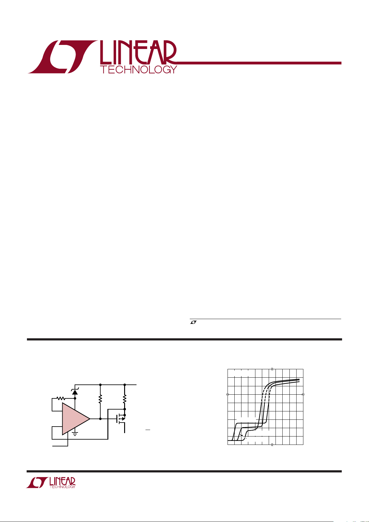
Over-The-Top Current Source with Shutdown
SHDN
I
OUT
LT1004-1.2
1M
*OPTIONAL FOR LOW OUTPUT CURRENTS
4V TO
44V
R
TPO610
1636 TA01
R*
–
+
LT1636
I
OUT
=
e.g., 10mA = 120Ω
1.2
R
■
Battery- or Solar-Powered Systems
Portable Instrumentation
Sensor Conditioning
■
Supply Current Sensing
■
Battery Monitoring
■
MUX Amplifiers
■
4mA to 20mA Transmitters
FEATURES
DESCRIPTIO
U
APPLICATIO S
U
TYPICAL APPLICATIO
U
Page 2
2
LT1636
1636fb
ABSOLUTE MAXIMUM RATINGS
W
WW
U
Total Supply Voltage (V+ to V–) .............................. 44V
Input Differential Voltage ......................................... 44V
Input Current ...................................................... ±25mA
Shutdown Pin Voltage Above V–............................. 32V
Shutdown Pin Current ....................................... ±10mA
Output Short-Circuit Duration (Note 2).........Continuous
Operating Temperature Range (Note 3)
LT1636C/LT1636I .............................. – 40°C to 85°C
LT1636H .......................................... – 40°C to 125°C
Specified Temperature Range (Note 4)
LT1636C/LT1636I .............................. – 40°C to 85°C
LT1636H .......................................... – 40°C to 125°C
Junction Temperature........................................... 150°C
Junction Temperature (DD Package) ................... 125°C
Storage Temperature Range ................. –65°C to 150°C
Storage Temperature Range
(DD Package) ....................................... – 65°C to 125°C
Lead Temperature (Soldering, 10 sec).................. 300°C
(Note 1)
ORDER PART
NUMBER
*The temperature grades are identified by a label on the shipping container. Consult factory for parts specified with wider operating temperature ranges.
ORDER PART
NUMBER
S8 PART
MARKING
1636
1636I
1636H
LT1636CN8
LT1636CS8
LT1636IN8
LT1636IS8
LT1636HS8
T
JMAX
= 150°C, θJA = 150°C/W (N8)
T
JMAX
= 150°C, θJA = 190°C/W (S8)
PACKAGE/ORDER I FOR ATIO
UUW
MS8 PART
MARKING
LTCL
LT1636CMS8
T
JMAX
= 150°C, θJA = 250°C/W
ORDER PART
NUMBER
DD PART*
MARKING
LAAJLT1636CDD
LT1636IDD
T
JMAX
= 125°C, θJA = 160°C/W (NOTE 2)
TOP VIEW
DD PACKAGE
8-LEAD (3mm × 3mm) PLASTIC DFN
5
6
7
8
4
3
2
1NULL
–IN
+IN
V
–
NULL
V
+
OUT
SHDN
1
2
3
4
8
7
6
5
TOP VIEW
MS8 PACKAGE
8-LEAD PLASTIC MSOP
NULL
–IN
+IN
V
–
NULL
V
+
OUT
SHDN
1
2
3
4
8
7
6
5
TOP VIEW
NULL
–IN
+IN
V
–
NULL
V
+
OUT
SHDN
N8 PACKAGE
8-LEAD PDIP
S8 PACKAGE
8-LEAD PLASTIC SO
LT1636C/LT1636I
SYMBOL PARAMETER CONDITIONS MIN TYP MAX UNITS
V
OS
Input Offset Voltage N8 Package 50 225 µV
0°C ≤ TA ≤ 70°C ● 400 µV
–40°C ≤ T
A
≤ 85°C ● 550 µV
S8 Package 50 225 µV
0°C ≤ TA ≤ 70°C ● 600 µV
–40°C ≤ T
A
≤ 85°C ● 750 µV
MS8 Package 50 225 µV
0°C ≤ TA ≤ 70°C ● 700 µV
–40°C ≤ T
A
≤ 85°C ● 850 µV
The ● denotes the specifications which apply over the full operating temperature range of –40°C ≤ TA ≤ 85°C.
VS = 3V, 0V; VS = 5V, 0V; VCM = V
OUT
= half supply unless otherwise specified. (Note 4)
3V 5VAUD ELECTRICAL CHARACTERISTICS
UNDERSIDE METAL CONNECTED TO V
–
Page 3
3
LT1636
1636fb
LT1636C/LT1636I
SYMBOL PARAMETER CONDITIONS MIN TYP MAX UNITS
DD Package 75 425 µV
0°C ≤ T
A
≤ 70°C ● 900 µV
–40°C ≤ TA ≤ 85°C ● 1050 µV
Input Offset Voltage Drift (Note 9) N8 Package, –40°C ≤ TA ≤ 85°C ● 15µV/°C
S8 Package, –40°C ≤ T
A
≤ 85°C ● 28µV/°C
MS8 Package, –40°C ≤ TA ≤ 85°C ● 210µV/°C
DD Package, –40°C ≤ T
A
≤ 85°C ● 210µV/°C
I
OS
Input Offset Current ● 0.1 0.8 nA
VCM = 44V (Note 5) ● 0.6 µA
I
B
Input Bias Current ● 58 nA
V
CM
= 44V (Note 5) ● 36 µA
V
S
= 0V 0.1 nA
Input Noise Voltage 0.1Hz to 10Hz 0.7 µV
P-P
e
n
Input Noise Voltage Density f = 1kHz 52 nV/√Hz
i
n
Input Noise Current Density f = 1kHz 0.035 pA/√Hz
R
IN
Input Resistance Differential 6 10 MΩ
Common Mode, VCM = 0V to 44V 7 15 MΩ
C
IN
Input Capacitance 4pF
Input Voltage Range ● 044V
CMRR Common Mode Rejection Ratio VCM = 0V to VCC – 1V ● 84 110 dB
(Note 5) V
CM
= 0V to 44V (Note 8) ● 86 98 dB
A
VOL
Large-Signal Voltage Gain VS = 3V, VO = 500mV to 2.5V, RL = 10k 200 1300 V/mV
V
S
= 3V, 0°C ≤ TA ≤ 70°C ● 133 V/mV
VS = 3V, –40°C ≤ TA ≤ 85°C ● 100 V/mV
VS = 5V, VO = 500mV to 4.5V, RL = 10k 400 2000 V/mV
V
S
= 5V, 0°C ≤ TA ≤ 70°C ● 250 V/mV
VS = 5V, –40°C ≤ TA ≤ 85°C ● 200 V/mV
V
OL
Output Voltage Swing LOW No Load ● 210 mV
I
SINK
= 5mA ● 480 875 mV
VS = 5V, I
SINK
= 10mA ● 860 1600 mV
V
OH
Output Voltage Swing HIGH VS = 3V, No Load ● 2.95 2.985 V
V
S
= 3V, I
SOURCE
= 5mA ● 2.55 2.8 V
VS = 5V, No Load ● 4.95 4.985 V
VS = 5V, I
SOURCE
= 10mA ● 4.30 4.75 V
I
SC
Short-Circuit Current (Note 2) VS = 3V, Short to GND 7 15 mA
V
S
= 3V, Short to V
CC
20 42 mA
VS = 5V, Short to GND 12 25 mA
V
S
= 5V, Short to V
CC
25 50 mA
PSRR Power Supply Rejection Ratio VS = 2.7V to 12.5V, VCM = VO = 1V ● 90 103 dB
Reverse Supply Voltage IS = –100µA ● 27 40 V
I
S
Supply Current (Note 6) 42 55 µA
● 60 µA
Supply Current, SHDN V
PIN5
= 2V, No Load (Note 6) ● 412 µA
I
SD
Shutdown Pin Current V
PIN5
= 0.3V, No Load (Note 6) ● 0.5 15 nA
V
PIN5
= 2V, No Load (Note 5) ● 1.1 5 µA
Output Leakage Current, SHDN V
PIN5
= 2V, No Load (Note 6) ● 0.05 1 µA
Maximum Shutdown Pin Current V
PIN5
= 32V, No Load (Note 5) ● 27 150 µA
t
ON
Turn-On Time V
PIN5
= 5V to 0V, RL = 10k 120 µs
t
OFF
Turn-Off Time V
PIN5
= 0V to 5V, RL = 10k 2.5 µs
The ● denotes the specifications which apply over the full operating temperature range of –40°C ≤ TA ≤ 85°C.
VS = 3V, 0V; VS = 5V, 0V; VCM = V
OUT
= half supply unless otherwise specified. (Note 4)
3V 5VAUD ELECTRICAL CHARACTERISTICS
Page 4
4
LT1636
1636fb
The ● denotes the specifications which apply over the full operating temperature range of –40°C ≤ TA ≤ 85°C.
VS = 3V, 0V; VS = 5V, 0V; VCM = V
OUT
= half supply unless otherwise specified. (Note 4)
3V 5VAUD ELECTRICAL CHARACTERISTICS
LT1636C/LT1636I
SYMBOL PARAMETER CONDITIONS MIN TYP MAX UNITS
GBW Gain Bandwidth Product f = 1kHz 110 200 kHz
(Note 5) 0°C ≤ T
A
≤ 70°C ● 100 kHz
–40°C ≤ TA ≤ 85°C ● 90 kHz
SR Slew Rate AV = –1, R
L
= ∞ 0.035 0.07 V/µs
(Note 7) 0°C ≤ T
A
≤ 70°C ● 0.031 V/µs
–40°C ≤ T
A
≤ 85°C ● 0.030 V/µs
LT1636C/LT1636I
SYMBOL PARAMETER CONDITIONS MIN TYP MAX UNITS
V
OS
Input Offset Voltage N8 Package 100 450 µV
0°C ≤ TA ≤ 70°C ● 550 µV
–40°C ≤ T
A
≤ 85°C ● 700 µV
S8 Package 100 450 µV
0°C ≤ TA ≤ 70°C ● 750 µV
–40°C ≤ T
A
≤ 85°C ● 900 µV
MS8 Package 100 450 µV
0°C ≤ TA ≤ 70°C ● 850 µV
–40°C ≤ TA ≤ 85°C ● 1000 µV
DD Package 125 650 µV
0°C ≤ T
A
≤ 70°C ● 1050 µV
–40°C ≤ TA ≤ 85°C ● 1200 µV
Input Offset Voltage Drift (Note 9) N8 Package, –40°C ≤ TA ≤ 85°C ● 1 4µV/°C
S8 Package, –40°C ≤ T
A
≤ 85°C ● 2 8 µV/°C
MS8 Package, –40°C ≤ TA ≤ 85°C ● 210µV/°C
DD Package, –40°C ≤ T
A
≤ 85°C ● 210µV/°C
I
OS
Input Offset Current ● 0.2 1.0 nA
I
B
Input Bias Current ● 410 nA
Input Noise Voltage 0.1Hz to 10Hz 1 µV
P-P
e
n
Input Noise Voltage Density f = 1kHz 52 nV/√Hz
i
n
Input Noise Current Density f = 1kHz 0.035 pA/√Hz
R
IN
Input Resistance Differential 5.2 13 MΩ
Common Mode, VCM = –15V to 14V 12000 MΩ
C
IN
Input Capacitance 4pF
Input Voltage Range ● –15 29 V
CMRR Common Mode Rejection Ratio VCM = –15V to 29V ● 86 103 dB
A
VOL
Large-Signal Voltage Gain VO = ±14V, RL = 10k 100 500 V/mV
0°C ≤ TA ≤ 70°C ● 75 V/mV
–40°C ≤ T
A
≤ 85°C ● 50 V/mV
V
OL
Output Voltage Swing LOW No Load ● –14.997 –14.95 V
I
SINK
= 5mA ● –14.500 –14.07 V
I
SINK
= 10mA ● –14.125 –13.35 V
V
OH
Output Voltage Swing HIGH No Load ● 14.9 14.975 V
I
SOURCE
= 5mA ● 14.5 14.750 V
I
SOURCE
= 10mA ● 14.3 14.650 V
The ● denotes the specifications which apply over the full operating temperature range of –40°C ≤ TA␣ ≤␣85°C.
VS = ±15V, VCM = 0V, V
OUT
= 0V, V
SHDN
= V– unless otherwise specified. (Note 4)
±15V ELECTRICAL CHARACTERISTICS
Page 5
5
LT1636
1636fb
LT1636C/LT1636I
SYMBOL PARAMETER CONDITIONS MIN TYP MAX UNITS
I
SC
Short-Circuit Current (Note 2) Short to GND ±18 ±30 mA
0°C ≤ T
A
≤ 70°C ● ±15 mA
–40°C ≤ T
A
≤ 85°C ● ±10 mA
PSRR Power Supply Rejection Ratio VS = ±1.35V to ±22V ● 90 114 dB
I
S
Supply Current 50 70 µA
● 85 µA
Positive Supply Current, SHDN V
PIN5
= –20V, VS = ±22V, No Load ● 12 30 µA
I
SHDN
Shutdown Pin Current V
PIN5
= –21.7V, VS = ±22V, No Load ● 0.7 15 nA
V
PIN5
= –20V, VS = ±22V, No Load ● 1.2 8 µA
Maximum Shutdown Pin Current V
PIN5
= 32V, VS = ±22V ● 27 150 µA
Output Leakage Current, SHDN V
PIN5
= –20V, VS = ±22V, No Load ● 0.1 2 µA
GBW Gain Bandwidth Product f = 1kHz 125 220 kHz
0°C ≤ T
A
≤ 70°C ● 110 kHz
–40°C ≤ T
A
≤ 85°C ● 100 kHz
SR Slew Rate AV = –1, R
L
= ∞, VO = ±10V Measured at ±5V 0.0375 0.075 V/µs
0°C ≤ T
A
≤ 70°C ● 0.033 V/µs
–40°C ≤ TA ≤ 85°C ● 0.030 V/µs
The ● denotes the specifications which apply over the full operating temperature range of –40°C ≤ TA␣ ≤␣85°C, otherwise
specifications are at TA = 25°C. VS = ±15V, VCM = 0V, V
OUT
= 0V, V
SHDN
= V– unless otherwise specified. (Note 4)
±15V ELECTRICAL CHARACTERISTICS
LT1636H
SYMBOL PARAMETER CONDITIONS MIN TYP MAX UNITS
V
OS
Input Offset Voltage 50 325 µV
● 3mV
Input Offset Voltage Drift (Note 9) ● 310µV/°C
I
OS
Input Offset Current ● 3nA
V
CM
= 44V (Note 5) ● 1 µA
I
B
Input Bias Current ● 30 nA
VCM = 44V (Note 5) ● 10 µA
Input Voltage Range ● 0.3 44 V
CMRR Common Mode Rejection Ratio VCM = 0.3V to VCC – 1V ● 72 dB
(Note 5) VCM = 0.3V to 44V ● 74 dB
A
VOL
Large-Signal Voltage Gain VS = 3V, VO = 500mV to 2.5V, RL = 10k 200 1300 V/mV
● 20 V/mV
VS = 5V, VO = 500mV to 4.5V, RL = 10k 400 2000 V/mV
● 35 V/mV
V
OL
Output Voltage Swing LOW No Load ● 15 mV
I
SINK
= 2.5mA ● 875 mV
V
OH
Output Voltage Swing HIGH VS = 3V, No Load ● 2.925 V
VS = 3V, I
SOURCE
= 5mA ● 2.35 V
VS = 5V, No Load ● 4.925 V
V
S
= 5V, I
SOURCE
= 10mA ● 4.10 V
PSRR Power Supply Rejection Ratio VS = 2.7V to 12.5V, VCM = VO = 1V ● 80 dB
Minimum Supply Voltage ● 2.7 V
The ● denotes the specifications which apply over the full operating temperature range of –40°C ≤ TA ≤ 125°C.
VS = 3V, 0V; VS = 5V, 0V; VCM = V
OUT
= half supply unless otherwise specified. (Note 4)
3V 5VAUD ELECTRICAL CHARACTERISTICS
Page 6

6
LT1636
1636fb
LT1636H
SYMBOL PARAMETER CONDITIONS MIN TYP MAX UNITS
Reverse Supply Voltage IS = –100µA ● 25 V
I
S
Supply Current (Note 6) 42 55 µA
● 75 µA
Supply Current, SHDN V
PIN5
= 2V, No Load (Note 6) ● 15 µA
I
SD
Shutdown Pin Current V
PIN5
= 0.3V, No Load (Note 6) ● 200 nA
V
PIN5
= 2V, No Load (Note 5) ● 7 µA
Output Leakage Current, SHDN V
PIN5
= 2V, No Load (Note 6) ● 5 µA
Maximum Shutdown Pin Current V
PIN5
= 32V, No Load (Note 5) ● 200 µA
GBW Gain Bandwidth Product f = 1kHz (Note 5) 110 200 kHz
● 60 kHz
SR Slew Rate AV = –1, R
L
= ∞ (Note 7) 0.035 0.07 V/µs
● 0.015 V/µs
The ● denotes the specifications which apply over the full operating temperature range of –40°C ≤ TA ≤ 125°C.
VS = 3V, 0V; VS = 5V, 0V; VCM = V
OUT
= half supply unless otherwise specified. (Note 4)
3V 5VAUD ELECTRICAL CHARACTERISTICS
The ● denotes the specifications which apply over the full operating temperature range of –40°C ≤ TA␣ ≤␣ 125°C.
VS = ±15V, VCM = 0V, V
OUT
= 0V, V
SHDN
= V– unless otherwise specified. (Note 4)
±15V ELECTRICAL CHARACTERISTICS
LT1636H
SYMBOL PARAMETER CONDITIONS MIN TYP MAX UNITS
V
OS
Input Offset Voltage 100 550 µV
● 3.4 mV
Input Offset Voltage Drift (Note 9) ● 3 11µV/°C
I
OS
Input Offset Current ● 5nA
I
B
Input Bias Current ● 50 nA
CMRR Common Mode Rejection Ratio VCM = –14.7V to 29V ● 72 dB
A
VOL
Large-Signal Voltage Gain VO = ±14V, RL = 10k 100 500 V/mV
● 4 V/mV
V
O
Output Voltage Swing No Load ● ±14.8 V
I
OUT
= ±2.5mA ● ±14.3 V
PSRR Power Supply Rejection Ratio VS = ±1.35V to ±22V ● 84 dB
Minimum Supply Voltage ● ±1.35 V
I
S
Supply Current 50 70 µA
● 100 µA
Positive Supply Current, SHDN V
PIN5
= –20V, VS = ±22V, No Load ● 40 µA
I
SHDN
Shutdown Pin Current V
PIN5
= –21.7V, VS = ±22V, No Load ● 200 nA
V
PIN5
= –20V, VS = ±22V, No Load ● 10 µA
Maximum Shutdown Pin Current V
PIN5
= 32V, VS = ±22V ● 200 µA
Output Leakage Current, SHDN V
PIN5
= –20V, VS = ±22V, No Load ● 100 µA
V
L
Shutdown Pin Input Low Voltage VS = ±22V ● –21.7 V
V
H
Shutdown Pin Input High Voltage VS = ±22V ● –20 V
GBW Gain Bandwidth Product f = 1kHz 125 220 kHz
● 75 kHz
SR Slew Rate AV = –1, R
L
= ∞, VO = ±10V 0.0375 0.075 V/µs
Measured at V
O
= ±5V ● 0.02 V/µs
Page 7

7
LT1636
1636fb
TYPICAL PERFOR A CE CHARACTERISTICS
UW
TOTAL SUPPLY VOLTAGE (V)
0
SUPPLY CURRENT (µA)
40
50
60
40352515545
1636 G01
30
20
0
10 20 30
10
80
70
TA = 125°C
TA = 25°C
T
A
= –55°C
Supply Current vs Supply Voltage
COMMON MODE VOLTAGE (V)
4.0
–10
INPUT BIAS CURRENT (nA)
0
20
30
40
5.2 10 20 30 40
5000
1636 G03
10
4.4 4.8 50
1000
3000
VS = 5V, 0V
TA = –55°C
T
A
= 125°C
TA = 25°C
Input Bias Current
vs Common Mode Voltage
SOURCING LOAD CURRENT (mA)
0.0001 0.001
0.01
OUTPUT SATURATION VOLTAGE (V)
0.1
1
0.01 0.1 1 10 100
1636 G04
VS = 5V
V
OD
= 30mV
TA = 125°C
T
A
= 25°C
T
A
= –55°C
Output Saturation Voltage
vs Load Current (Output High)
INPUT OVERDRIVE (mV)
0
OUTPUT SATURATION VOLTAGE (mV)
60
80
100
80
1636 G06
40
20
50
70
90
30
10
0
20
40
60
10 90
30
50
70
100
OUTPUT HIGH
OUTPUT LOW
VS = ±2.5V
NO LOAD
Output Saturation Voltage
vs Input Overdrive
Output Saturation Voltage
vs Load Current (Output Low)
SINKING LOAD CURRENT (mA)
0.0001 0.001
0.001
0.01
OUTPUT SATURATION VOLTAGE (V)
0.1
1
10
0.01 0.1 1 10 100
1636 G05
VS = 5V
V
OD
= 30mV
TA = 125°C
T
A
= –55°C
TA = 25°C
Minimum Supply Voltage
TOTAL SUPPLY VOLTAGE (V)
CHANGE IN INPUT OFFSET VOLTAGE (µV)
–300
–100
300
–200
200
100
0
1234
1636 G02
50
TA = –55°CTA = 125°C
TA = 25°C
Note 1: Absolute Maximum Ratings are those values beyond which the life
of a device may be impaired.
Note 2: A heat sink may be required to keep the junction temperature
below absolute maximum. The θ
JA
specified for the DD package is with
minimal PCB heat spreading metal. A significant reduction in θ
JA
can be
obtained with expanded PCB metal area on all layers of a board.
Note 3: The LT1636C and LT1636I are guaranteed functional over the
operating temperature range of –40°C to 85°C. The LT1636H is
guaranteed functional over the operating temperature range of –40°C to
125°C.
Note 4: The LT1636C is guaranteed to meet specified performance from
0°C to 70°C. The LT1636C is designed, characterized and expected to
meet specified performance from –40°C to 85°C but is not tested or QA
sampled at these temperatures. The LT1636I is guaranteed to meet
specified performance from –40°C to 85°C. The LT1636H is guaranteed to
meet specified performance from –40°C to 125°C.
Note 5: V
S
= 5V limits are guaranteed by correlation to VS = 3V and
V
S
= ±15V or VS = ±22V tests.
Note 6: VS = 3V limits are guaranteed by correlation to VS = 5V and
V
S
= ±15V or VS = ±22V tests.
Note 7: Guaranteed by correlation to slew rate at VS = ±15V and GBW at
V
S
= 3V and VS = ±15V tests.
Note 8: This specification implies a typical input offset voltage of 600µV at
V
CM
= 44V and a maximum input offset voltage of 3mV at VCM = 44V.
Note 9: This parameter is not 100% tested.
ELECTRICAL CHARACTERISTICS
Page 8

8
LT1636
1636fb
TYPICAL PERFOR A CE CHARACTERISTICS
UW
FREQUENCY (Hz)
1k
10
GAIN (dB)
PHASE SHIFT (DEG)
20
30
40
50
10k 100k 1M
1636 G10
0
–10
–20
–30
60
70
–20
0
20
40
60
–40
–60
–80
–100
80
100
VS = ±2.5V
PHASE
GAIN
Open-Loop Gain and Phase Shift
vs Frequency
TEMPERATURE (°C)
–50
SLEW RATE (V/µs)
0.09
0.10
0.11
25
1636 G12
0.08
0.07
–25 0 50 75 100 125
0.06
0.05
0.04
0.12
RISING, VS = ±1.5V
FALLING, V
S
= ±1.5V
FALLING, V
S
= ±15V
RISING, VS = ±15V
Slew Rate vs Temperature
TEMPERATURE (°C)
–50
GAIN-BANDWIDTH PRODUCT (kHz)
220
240
260
25 75
1636 G11
200
180
–25 0
50 100 125
160
140
f = 1kHZ
V
S
= ±15V
V
S
= ±1.5V
Gain-Bandwidth Product
vs Temperature
Gain-Bandwidth Product and
Phase Margin vs Supply Voltage
TOTAL SUPPLY VOLTAGE (V)
0
180
GAIN-BANDWIDTH PRODUCT (kHz)
PHASE MARGIN (DEG)
200
240
260
280
10
20
25 45
1636 G13
220
515
30
35
40
300
20
40
30
50
PHASE MARGIN
GAIN BANDWIDTH
RL = 10k
f = 1kHz
CMRR vs Frequency PSRR vs Frequency
FREQUENCY (Hz)
1k
–20
POWER SUPPLY REJECTION RATIO (dB)
0
20
40
60
10k 100k
1636 G15
–10
10
30
50
70
80
VS = ±2.5V
POSITIVE SUPPLY
NEGATIVE SUPPLY
FREQUENCY (Hz)
1K
20
COMMON MODE REJECTION RATIO (dB)
40
60
80
100
10K 100K
1636 G14
30
50
70
90
110
120
VS = ±15V
V
S
= ±1.5V
FREQUENCY (Hz)
1
0.20
INPUT NOISE CURRENT DENSITY (pA/√Hz)
0.25
0.30
0.35
10 100 1000
1635 G09
0.15
0.10
0.05
0
Input Noise Current vs Frequency
TIME (SEC)
NOISE VOLTAGE (400nV/DIV)
2468
1636 G07
10103579
VS = ±2.5V
0.1Hz to 10Hz Noise Voltage
FREQUENCY (Hz)
1
30
INPUT NOISE VOLTAGE DENSITY (nV/√Hz)
60
70
80
10 100 1000
1636 G08
50
40
Noise Voltage Density
vs Frequency
Page 9

9
LT1636
1636fb
TYPICAL PERFOR A CE CHARACTERISTICS
UW
Settling Time to 0.1%
vs Output Step
Total Harmonic Distortion + Noise
vs Frequency
CAPACITIVE LOAD (pF)
10
40
OVERSHOOT (%)
50
60
70
80
100 1000 10000
1636 G20
30
20
10
0
90
100
VS = ±2.5V
I
SOURCE
= 40µA
NO OUTPUT COMPENSATION
AV = 1
AV = 5
A
V
= 2
AV = 10
Capacitive Load Handling,
Overshoot vs Capacitive Load
LOAD RESISTANCE TO GROUND (Ω)
0.01
THD + NOISE (%)
0.1
1
10
1k 10k 100k
1636 G22
0.001
100
VS = 3V TOTAL
A
V
= 1
V
IN
= 2V
P-P
AT 1kHz
VS = 3V, 0V
V
IN
= 0.2V TO 2.2V
VS = ±1.5V
V
IN
= ±1V
VS = 3V, 0V
V
IN
= 0.5V TO 2.5V
Total Harmonic Distortion + Noise
vs Load Resistance
Total Harmonic Distortion + Noise
vs Output Voltage
OUTPUT VOLTAGE (V
P-P
)
0.01
THD + NOISE (%)
1
10
023
1636 G23
0.001
1
0.1
RL = 10k
V
CM
= HALF SUPPLY
f = 1kHz
AV = –1
V
S
= ±1.5V
AV = –1
V
S
= 3V, 0V
AV = 1
V
S
= 3V, 0V
AV = 1
V
S
= ±1.5V
SETTLING TIME (µs)
0
–10
OUTPUT STEP (V)
–8
–4
–2
0
10
4
40
80
100
1636 G19
–6
6
8
2
20 60
120
140
160
AV = 1
AV = 1
A
V
= –1
VS = ±15V
AV = –1
FREQUENCY (Hz)
0.01
THD + NOISE (%)
0.1
1
10
100 1k 10k
1636 G21
0.001
10
VS = 3V, 0V
V
OUT
= 2V
P-P
VCM = 1.2V
R
L
= 50k
AV = –1
AV = 1
LOAD RESISTANCE (Ω)
1k
50
GAIN-BANDWIDTH PRODUCT (kHz)
PHASE MARGIN (DEG)
100
150
200
250
450
10k 100k
1636 G16
300
350
400
0
10
20
30
40
80
50
60
70
PHASE MARGIN
GAIN BANDWIDTH
VS = ±2.5V
Gain-Bandwidth Product and
Phase Margin vs Load Resistance
FREQUENCY (Hz)
100
20
OUTPUT SWING (V
P-P
)
25
30
35
1k 10k 100k
1635 G18
15
10
5
0
Vs = ±15V
Vs = ±2.5V
DISTORTION ≤ 1%
A
V
= 1
Undistorted Output Swing
vs Frequency
FREQUENCY (Hz)
100
0.1
OUTPUT IMPEDANCE (Ω)
10
10k
1k 100k10k
1635 G17
1
100
1k
VS = ±2.5V
AV = 100
A
V
= 10
AV = 1
Output Impedance vs Frequency
Page 10

10
LT1636
1636fb
TYPICAL PERFOR A CE CHARACTERISTICS
UW
CHANGE IN INPUT OFFSET VOLTAGE
(100µV/DIV)
Open-Loop Gain
0V 10V
OUTPUT VOLTAGE (5V/DIV)
A
B
C
C
1636 G24
VS = ±15V
A
V
= –1
1636 G25
A: RL = 2k
B: R
L
= 10k
C: R
L
= 50k
Large-Signal Response
VS = ±15V
A
V
= 1
1636 G26
Small-Signal Response
APPLICATIONS INFORMATION
WUU
U
cause the voltage at which operation switches from the
PNP stage to the NPN stage to move towards V+. The input
offset voltage of the NPN stage is untrimmed and is
typically 600µV.
A Schottky diode in the collector of each NPN transistor of
the NPN input stage allows the LT1636 to operate with
either or both of its inputs above V+. At about 0.3V above
V+ the NPN input transistor is fully saturated and the input
bias current is typically 3µA at room temperature. The
input offset voltage is typically 600µV when operating
above V+. The LT1636 will operate with its input 44V above
V– regardless of V+.
The inputs are protected against excursions as much as
22V below V– by an internal 1k resistor in series with each
input and a diode from the input to the negative supply.
There is no output phase reversal for inputs up to 5V below
V–. There are no clamping diodes between the inputs and
the maximum differential input voltage is 44V.
Output
The output voltage swing of the LT1636 is affected by input overdrive as shown in the typical performance curves.
When monitoring voltages within 100mV of V+, gain
should be taken to keep the output from clipping.
The output of the LT1636 can be pulled up to 27V beyond
V+ with less than 1nA of leakage current, provided that V
+
is less than 0.5V.
Supply Voltage
The positive supply pin of the LT1636 should be bypassed
with a small capacitor (about 0.01µF) within an inch of the
pin. When driving heavy loads an additional 4.7µF electro-
lytic capacitor should be used. When using split supplies,
the same is true for the negative supply pin.
The LT1636 is protected against reverse battery voltages
up to 27V. In the event a reverse battery condition occurs,
the supply current is less than 1nA.
When operating the LT1636 on total supplies of 20V or
more, the supply must not be brought up faster than 1µs.
This is especially true if low ESR bypass capacitors are
used. A series RLC circuit is formed from the supply lead
inductance and the bypass capacitor. 5Ω of resistance in
the supply or the bypass capacitor will dampen the tuned
circuit enough to limit the rise time.
Inputs
The LT1636 has two input stages, NPN and PNP (see
Simplified Schematic), resulting in three distinct operating regions as shown in the Input Bias Current vs Common
Mode typical performance curve.
For input voltages about 0.8V or more below V+, the PNP
input stage is active and the input bias current is typically
–4nA. When the input voltage is about 0.5V or less from
V+, the NPN input stage is operating and the input bias
current is typically 10nA. Increases in temperature will
A
B
–10VV
S
= ±15V
Page 11

11
LT1636
1636fb
APPLICATIONS INFORMATION
WUU
U
The normally reverse biased substrate diode from the
output to V– will cause unlimited currents to flow when the
output is forced below V–. If the current is transient and
limited to 100mA, no damage will occur.
The LT1636 is internally compensated to drive at least
200pF of capacitance under any output loading conditions. A 0.22µF capacitor in series with a 150Ω resistor
between the output and ground will compensate these
amplifiers for larger capacitive loads, up to 10,000pF, at
all output currents.
Distortion
There are two main contributors of distortion in op amps:
output crossover distortion as the output transitions from
sourcing to sinking current and distortion caused by
nonlinear common mode rejection. Of course, if the op
amp is operating inverting there is no common mode
induced distortion. When the LT1636 switches between
input stages there is significant nonlinearity in the CMRR.
Lower load resistance increases the output crossover
distortion, but has no effect on the input stage transition
distortion. For lowest distortion the LT1636 should be
operated single supply, with the output always sourcing
current and with the input voltage swing between ground
and (V+ – 0.8V). See the Typical Performance Characteristics curves.
Gain
The open-loop gain is less sensitive to load resistance
when the output is sourcing current. This optimizes performance in single supply applications where the load is
returned to ground. The typical performance photo of
Open-Loop Gain for various loads shows the details.
Shutdown
The LT1636 can be shut down two ways: using the
shutdown pin or bringing V+ to within 0.5V of V–. When V
+
is brought to within 0.5V of V– both the supply current and
output leakage current drop to less than 1nA. When the
shutdown pin is brought 1.2V above V–, the supply
current drops to about 4µA and the output leakage current
is less than 1µA, independent of V+. In either case the input
bias current is less than 0.1nA (even if the inputs are 44V
above the negative supply).
The shutdown pin can be taken up to 32V above V–. The
shutdown pin can be driven below V–, however the pin
current through the substrate diode should be limited with
an external resistor to less than 10mA.
Input Offset Nulling
The input offset voltage can be nulled by placing a 10k
potentiometer between Pins 1 and 8 with its wiper to V
–
(see Figure 1). The null range will be at least ±1mV.
LT1636
10k
1636 F01
V
–
1
8
Figure 1. Input Offset Nulling
Page 12

12
LT1636
1636fb
TYPICAL APPLICATIONS
U
MUX Amplifier
MUX Amplifier Waveforms
–
+
LT1636
74HC04
1636 TA05
V
IN1
V
OUT
V
IN2
INPUT
SELECT
SHDN
5V
5V
–
+
LT1636
SHDN
VS = 5V
V
IN1
= 1.2kHz AT 4V
P-P
, V
IN2
= 2.4kHz AT 2V
P-P
INPUT SELECT = 120Hz AT 5V
P-P
–
+
LT1636
1636 TA09
V
IN
0.22µF
C
L
≤ 10,000pF
150Ω
Optional Output Compensation for
Capacitive Loads Greater Than 200pF
Page 13

13
LT1636
1636fb
7
V
+
4
V
–
6
OUT
81
NULLNULL
1636 SS
3
5
+IN
–IN
Q25
Q24
Q26
Q18
Q17
R6
40k
R8
300Ω
R5
40k
R3
1k
R4
1k
SHDN
R7
300Ω
Q16
Q15Q10
Q11
Q9
Q8
Q14
Q2
D5
D2
Q13Q1
2µA
Q20
Q23
D3
Q7
D1
D4
Q6
Q4
Q5
2
R2
30k
R1
1M
Q3
Q19
Q21
Q22
Q12
SCHEMATIC
WW
SI PLIFIED
Page 14

14
LT1636
1636fb
PACKAGE DESCRIPTION
U
DD Package
8-Lead Plastic DFN (3mm × 3mm)
(Reference LTC DWG # 05-08-1698)
MS8 Package
8-Lead Plastic MSOP
(Reference LTC DWG # 05-08-1660)
3.00 ±0.10
(4 SIDES)
NOTE:
1. DRAWING TO BE MADE A JEDEC PACKAGE OUTLINE M0-229 VARIATION OF (WEED-1)
2. ALL DIMENSIONS ARE IN MILLIMETERS
3. DIMENSIONS OF EXPOSED PAD ON BOTTOM OF PACKAGE DO NOT INCLUDE
MOLD FLASH. MOLD FLASH, IF PRESENT, SHALL NOT EXCEED 0.15mm ON ANY SIDE
4. EXPOSED PAD SHALL BE SOLDER PLATED
0.38 ± 0.10
BOTTOM VIEW—EXPOSED PAD
1.65 ± 0.10
(2 SIDES)
0.75 ±0.05
R = 0.115
TYP
2.38 ±0.10
(2 SIDES)
14
85
PIN 1
TOP MARK
0.200 REF
0.00 – 0.05
(DD8) DFN 0203
0.28 ± 0.05
2.38 ±0.05
(2 SIDES)
RECOMMENDED SOLDER PAD PITCH AND DIMENSIONS
1.65 ±0.05
(2 SIDES)2.15 ±0.05
0.50
BSC
0.675 ±0.05
3.5 ±0.05
PACKAGE
OUTLINE
0.28 ± 0.05
0.50 BSC
MSOP (MS8) 0802
0.53 ± 0.015
(.021 ± .006)
SEATING
PLANE
NOTE:
1. DIMENSIONS IN MILLIMETER/(INCH)
2. DRAWING NOT TO SCALE
3. DIMENSION DOES NOT INCLUDE MOLD FLASH, PROTRUSIONS OR GATE BURRS.
MOLD FLASH, PROTRUSIONS OR GATE BURRS SHALL NOT EXCEED 0.152mm (.006") PER SIDE
4. DIMENSION DOES NOT INCLUDE INTERLEAD FLASH OR PROTRUSIONS.
INTERLEAD FLASH OR PROTRUSIONS SHALL NOT EXCEED 0.152mm (.006") PER SIDE
5. LEAD COPLANARITY (BOTTOM OF LEADS AFTER FORMING) SHALL BE 0.102mm (.004") MAX
0.18
(.077)
0.254
(.010)
1.10
(.043)
MAX
0.22 – 0.38
(.009 – .015)
TYP
0.13 ± 0.076
(.005 ± .003)
0.86
(.034)
REF
0.65
(.0256)
BSC
0
° – 6° TYP
DETAIL “A”
DETAIL “A”
GAUGE PLANE
12
3
4
4.90
± 0.15
(1.93 ± .006)
8
7
6
5
3.00 ± 0.102
(.118 ± .004)
(NOTE 3)
3.00 ± 0.102
(.118 ± .004)
NOTE 4
0.52
(.206)
REF
5.23
(.206)
MIN
3.2 – 3.45
(.126 – .136)
0.889
± 0.127
(.035 ± .005)
RECOMMENDED SOLDER PAD LAYOUT
0.42 ± 0.04
(.0165 ± .0015)
TYP
0.65
(.0256)
BSC
Page 15

15
LT1636
1636fb
Information furnished by Linear Technology Corporation is believed to be accurate and reliable.
However, no responsibility is assumed for its use. Linear Technology Corporation makes no representation that the interconnection of its circuits as described herein will not infringe on existing patent rights.
PACKAGE DESCRIPTION
U
N8 Package
8-Lead PDIP (Narrow .300 Inch)
(Reference LTC DWG # 05-08-1510)
S8 Package
8-Lead Plastic Small Outline (Narrow .150 Inch)
(Reference LTC DWG # 05-08-1610)
N8 1002
.065
(1.651)
TYP
.045 – .065
(1.143 – 1.651)
.130 ± .005
(3.302 ± 0.127)
.020
(0.508)
MIN
.018 ± .003
(0.457 ± 0.076)
.120
(3.048)
MIN
1234
876
5
.255 ± .015*
(6.477 ± 0.381)
.400*
(10.160)
MAX
.008 – .015
(0.203 – 0.381)
.300 – .325
(7.620 – 8.255)
.325
+.035
–.015
+0.889
–0.381
8.255
()
NOTE:
1. DIMENSIONS ARE
INCHES
MILLIMETERS
*THESE DIMENSIONS DO NOT INCLUDE MOLD FLASH OR PROTRUSIONS.
MOLD FLASH OR PROTRUSIONS SHALL NOT EXCEED .010 INCH (0.254mm)
.100
(2.54)
BSC
.016 – .050
(0.406 – 1.270)
.010 – .020
(0.254 – 0.508)
× 45°
0°– 8° TYP
.008 – .010
(0.203 – 0.254)
SO8 0502
.053 – .069
(1.346 – 1.752)
.014 – .019
(0.355 – 0.483)
TYP
.004 – .010
(0.101 – 0.254)
.050
(1.270)
BSC
1
N
2
3
4
N/2
.150 – .157
(3.810 – 3.988)
NOTE 3
8
7
6
5
.189 – .197
(4.801 – 5.004)
NOTE 3
.228 – .244
(5.791 – 6.197)
.245
MIN
N
1 2 3 N/2
.160 ±.005
RECOMMENDED SOLDER PAD LAYOUT
.045 ±.005
.050 BSC
.030 ±.005
TYP
INCHES
(MILLIMETERS)
NOTE:
1. DIMENSIONS IN
2. DRAWING NOT TO SCALE
3. THESE DIMENSIONS DO NOT INCLUDE MOLD FLASH OR PROTRUSIONS.
MOLD FLASH OR PROTRUSIONS SHALL NOT EXCEED .006" (0.15mm)
Page 16

16
LT1636
1636fb
LT/TP 0303 1K REV B • PRINTED IN USA
LINEAR TECHNOLOGY CORPORATION 1998
Linear Technology Corporation
1630 McCarthy Blvd., Milpitas, CA 95035-7417
(408) 432-1900 ● FAX: (408) 434-0507
●
www.linear.com
TYPICAL APPLICATIONS
U
RELATED PARTS
Lamp Outage Detector Over-The-Top Current Sense
–
+
LT1636
5V TO 44V
5V
R1
200Ω
R
S
0.2Ω
R2
2k
V
OUT
(0V TO 4.3V)
1636 TA08
LOAD
I
LOAD
V
OUT
(RS)(R2/R1)
I
LOAD
=
–
+
LT1636
IN1
(0V TO 44V)
IN2
(0V TO 44V)
2N5087
2N5210
1636 TA03
1M
V
OUT
1M
V
CC
100
1M
10k
HYSTERESIS =
10k
1M
3V TO 44V
Over-The-Top Comparator with Hysteresis
Self-Buffered Micropower Reference
–
+
LT1636
1636 TA04
V
OUT
= 1.25V
I
OUT
≤ 10mA
1N5711
LT1634-1.25
0.1µF
1M
4V TO 44V
–
+
LT1636
5k
1M
5V TO 44V
3V
100k
0.5Ω
LAMP
ON/OFF
OUT
1636 TA07
OUT = 0V FOR GOOD BULB
3V FOR OPEN BULB
PART NUMBER DESCRIPTION COMMENTS
LT1078/LT1079 Dual/Quad 55µA Max, Single Supply, Precision Op Amps Input/Output Common Mode Includes Ground, 70µV V
OS(MAX)
LT2078/LT2079 and 2.5µV/°C Drift (Max), 200kHz GBW, 0.07V/µs Slew Rate
LT1178/LT1179 Dual/Quad 17µA Max, Single Supply, Precison Op Amps Input/Output Common Mode Includes Ground, 70µV V
OS(MAX)
LT2178/LT2179 and 4µV/°C Drift (Max), 85kHz GBW, 0.04V/µs Slew Rate
LT1366/LT1367 Dual/Quad Precision, Rail-to-Rail Input and Output Op Amps 475µV V
OS(MAX)
, 500V/mV A
VOL(MIN)
, 400kHz GBW
LT1490/LT1491 Dual/Quad Over-The-Top Micropower, Rail-to-Rail Input and Single Supply Input Range: – 0.4V to 44V, Micropower 50µA
Output Op Amps per Amplifier, Rail-to-Rail Input and Output, 200kHz GBW
LT1637 Single Over-The-Top Micropower Rail-to-Rail Input and Output 1.1MHz, V
CM
Extends 44V above VEE,
Op Amp Independent of VCC; MSOP Package, Shutdown Function
LT1638/LT1639 Dual/Quad 1.2MHz Over-The-Top Micropower, Rail-to-Rail 0.4V/µs Slew Rate, 230µA Supply Current per Amplifier
Input and Output Op Amps
LT1782 Micropower, Over-The-Top, SOT-23, Rail-to-Rail SOT-23, 800µV V
OS(MAX)
, IS = 55µA (Max),
Input and Output Op Amp Gain-Bandwidth = 200kHz, Shutdown Pin
LT1783 1.2MHz, Over-The-Top, Micropower, Rail-to-Rail SOT-23, 800µV V
OS(MAX)
, IS = 300µA (Max),
Input and Output Op Amp Gain-Bandwidth = 1.2MHz, Shutdown Pin
 Loading...