

Page 1
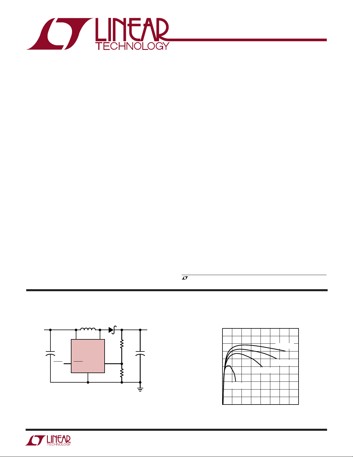
LOAD CURRENT (mA)
0 50 100 150 200 250 300 350 400
EFFICIENCY (%)
1613 TA01a
100
95
90
85
80
75
70
65
60
55
50
VIN = 4.2V
VIN = 3.5V
VIN = 2.8V
VIN = 1.5V
FEATURES
■
Uses Tiny Capacitors and Inductor
■
Internally Compensated
■
Fixed Frequency 1.4MHz Operation
■
Operates with VIN as Low as 1.1V
■
3V at 30mA from a Single Cell
■
5V at 200mA from 3.3V Input
■
15V at 60mA from Four Alkaline Cells
■
High Output Voltage: Up to 34V
■
Low Shutdown Current: <1µA
■
Low V
■
Tiny 5-Lead SOT-23 Package
Switch: 300mV at 300mA
CESAT
U
APPLICATIO S
■
Digital Cameras
■
Pagers
■
Cordless Phones
■
Battery Backup
■
LCD Bias
■
Medical Diagnostic Equipment
■
Local 5V or 12V Supply
■
External Modems
■
PC Cards
LT1613
1.4MHz, Single Cell DC/DC
Converter in 5-Lead SOT-23
U
DESCRIPTIO
The LT®1613 is the industry’s first 5-lead SOT-23 current
mode DC/DC converter. Intended for small, low power
applications, it operates from an input voltage as low as
1.1V and switches at 1.4MHz, allowing the use of tiny, low
cost capacitors and inductors 2mm or less in height. Its
small size and high switching frequency enables the
complete DC/DC converter function to take up less than
0.2 square inches of PC board area. Multiple output power
supplies can now use a separate regulator for each output
voltage, replacing cumbersome quasi-regulated approaches using a single regulator and a custom transformer.
A constant frequency, internally compensated current
mode PWM architecture results in low, predictable output
noise that is easy to filter. The high voltage switch on the
LT1613 is rated at 36V, making the device ideal for boost
converters up to 34V as well as for Single-Ended Primary
Inductance Converter (SEPIC) and flyback designs. The
device can generate 5V at up to 200mA from a 3.3V supply
or 5V at 175mA from four alkaline cells in a SEPIC design.
The LT1613 is available in the 5-lead SOT-23 package.
, LTC and LT are registered trademarks of Linear Technology Corporation.
TYPICAL APPLICATIO
V
IN
3.3V
+ +
C1
15µF
L1: MURATA LQH3C4R7M24 OR SUMIDA CD43-4R7
C1: AVX TAJA156M010
C2: AVX TAJB226M006
D1: MBR0520
Figure 1. 3.3V to 5V 200mA DC/DC Converter
4.7µH
V
IN
LT1613
SHDN
L1
GND
SW
U
D1
V
OUT
5V
R1
37.4k
FBSHDN
R2
12.1k
200mA
C2
22µF
1613 TA01
Efficiency Curve
1
Page 2

LT1613
WW
W
ABSOLUTE MAXIMUM RA TIN GS
(Note 1)
VIN Voltage .............................................................. 10V
SW Voltage................................................–0.4V to 36V
FB Voltage ..................................................... VIN + 0.3V
Current into FB Pin ............................................... ±1mA
SHDN Voltage.......................................................... 10V
Maximum Junction Temperature..........................125°C
Operating Temperature Range
Commercial .............................................0°C to 70°C
U
U
W
PACKAGE/ORDER INFORMATION
ORDER PART NUMBER
TOP VIEW
SW 1
GND 2
FB 3
S5 PACKAGE
5-LEAD PLASTIC SOT-23
5 V
IN
4 SHDN
LT1613CS5
S5 PART MARKING
LTED
U
Extended Commercial (Note 2)........... –40°C to 85°C
Storage Temperature Range................. –65°C to 150°C
Lead Temperature (Soldering, 10 sec)..................300°C
Consult factory for Industrial and Military grade parts.
ELECTRICAL CHARACTERISTICS
temperature range, otherwise specifications are at TA = 25°C. Commercial grade 0°C to 70°C, VIN = 1.5V, V
otherwise noted. (Note 2)
PARAMETER CONDITIONS MIN TYP MAX UNITS
Minimum Operating Voltage 0.9 1.1 V
Maximum Operating Voltage 10 V
Feedback Voltage ● 1.205 1.23 1.255 V
FB Pin Bias Current ● 27 80 nA
Quiescent Current V
Quiescent Current in Shutdown V
Reference Line Regulation 1.5V ≤ VIN ≤ 10V 0.02 0.2 %/V
Switching Frequency ● 1.0 1.4 1.8 MHz
Maximum Duty Cycle ● 82 86 %
Switch Current Limit (Note 3) 550 800 mA
Switch V
CESAT
Switch Leakage Current VSW = 5V 0.01 1 µA
SHDN Input Voltage High 1V
SHDN Input Voltage Low 0.3 V
SHDN Pin Bias Current V
Note 1: Absolute Maximum Ratings are those values beyond which the life
of a device may be impaired.
= 1.5V 3 4.5 mA
SHDN
= 0V, VIN = 2V 0.01 0.5 µA
SHDN
= 0V, VIN = 5V 0.01 1.0 µA
V
SHDN
ISW = 300mA 300 350 mV
= 3V 25 50 µA
SHDN
V
= 0V 0.01 0.1 µA
SHDN
The ● denotes the specifications which apply over the full operating
= VIN unless
SHDN
Note 2: The LT1613C is guaranteed to meet performance specifications
from 0°C to 70°C. Specifications over the –40°C to 85°C operating
temperature range are assured by design, characterization and correlation
with statistical process controls.
Note 3: Current limit guaranteed by design and/or correlation to static test.
2
Page 3
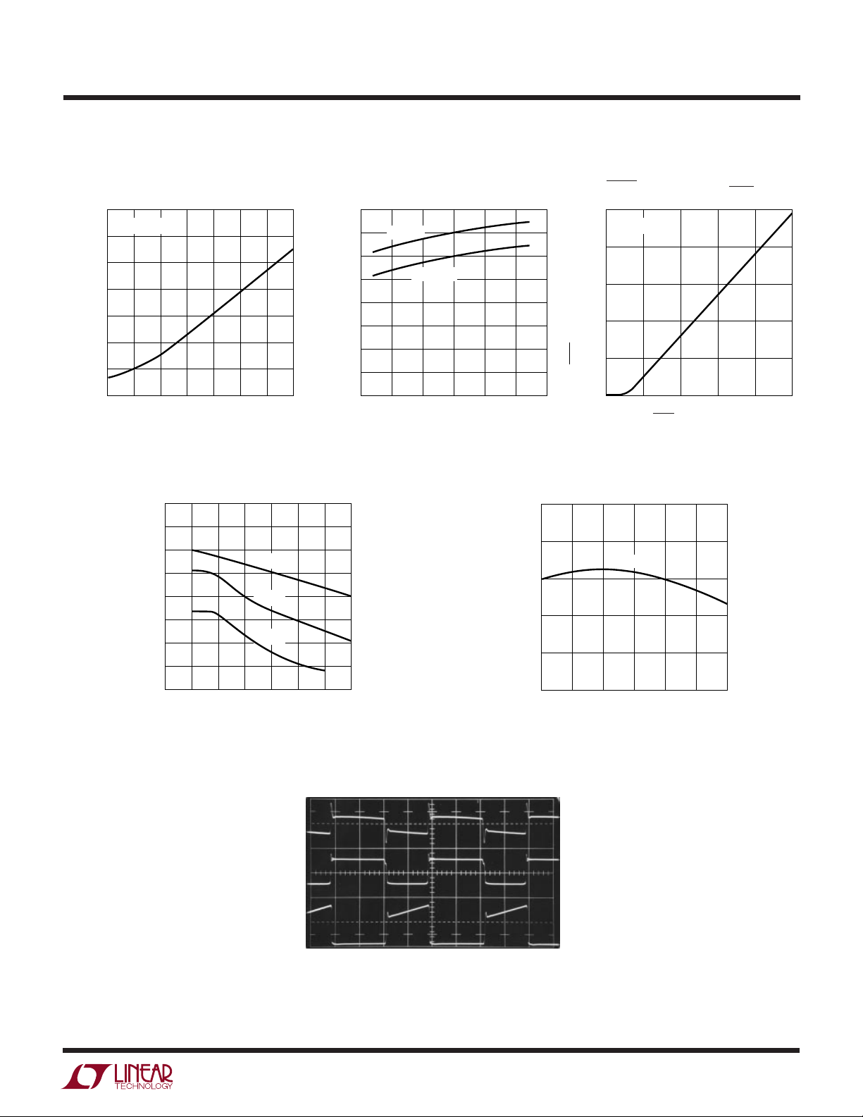
UW
TEMPERATURE (°C)
–50
FEEDBACK PIN VOLTAGE (V)
1613 G05
1.25
1.24
1.23
1.22
1.21
1.20
VOLTAGE
–25 0 25 50 75 100
TYPICAL PERFOR A CE CHARACTERISTICS
Oscillator Frequency vs
Switch V
700
TA = 25°C
600
500
400
(mV)
300
CESAT
V
200
100
0
0 100 200 300 400 500 600 700
vs Switch Current SHDN Pin Current vs V
CESAT
SWITCH CURRENT (mA)
1613 G01
Temperature
2.00
1.75
1.50
1.25
1.00
0.75
0.50
SWITCHING FREQUENCY (MHz)
0.25
VIN = 5V
VIN = 1.5V
0
–50 –25 0 25 50 75 100
TEMPERATURE (°C)
1613 G02
LT1613
SHDN
50
TA = 25°C
40
30
20
10
SHDN PIN BIAS CURRENT (µA)
0
012345
SHDN PIN VOLTAGE (V)
1613 G03
Current Limit vs Duty Cycle
1000
900
800
700
600
500
CURRENT LIMIT (mA)
400
300
200
10 20 30 40 50 60 70 80
70°C
25°C
–40°C
DUTY CYCLE (%)
V
100mV/DIV
AC COUPLED
V
5V/DIV
Feedback Pin Voltage
1613 G04
Switching Waveforms, Circuit of Figure 1
OUT
SW
I
SW
200mA/DIV
= 150mA 200ns/DIV 1613 G06
I
LOAD
3
Page 4
LT1613
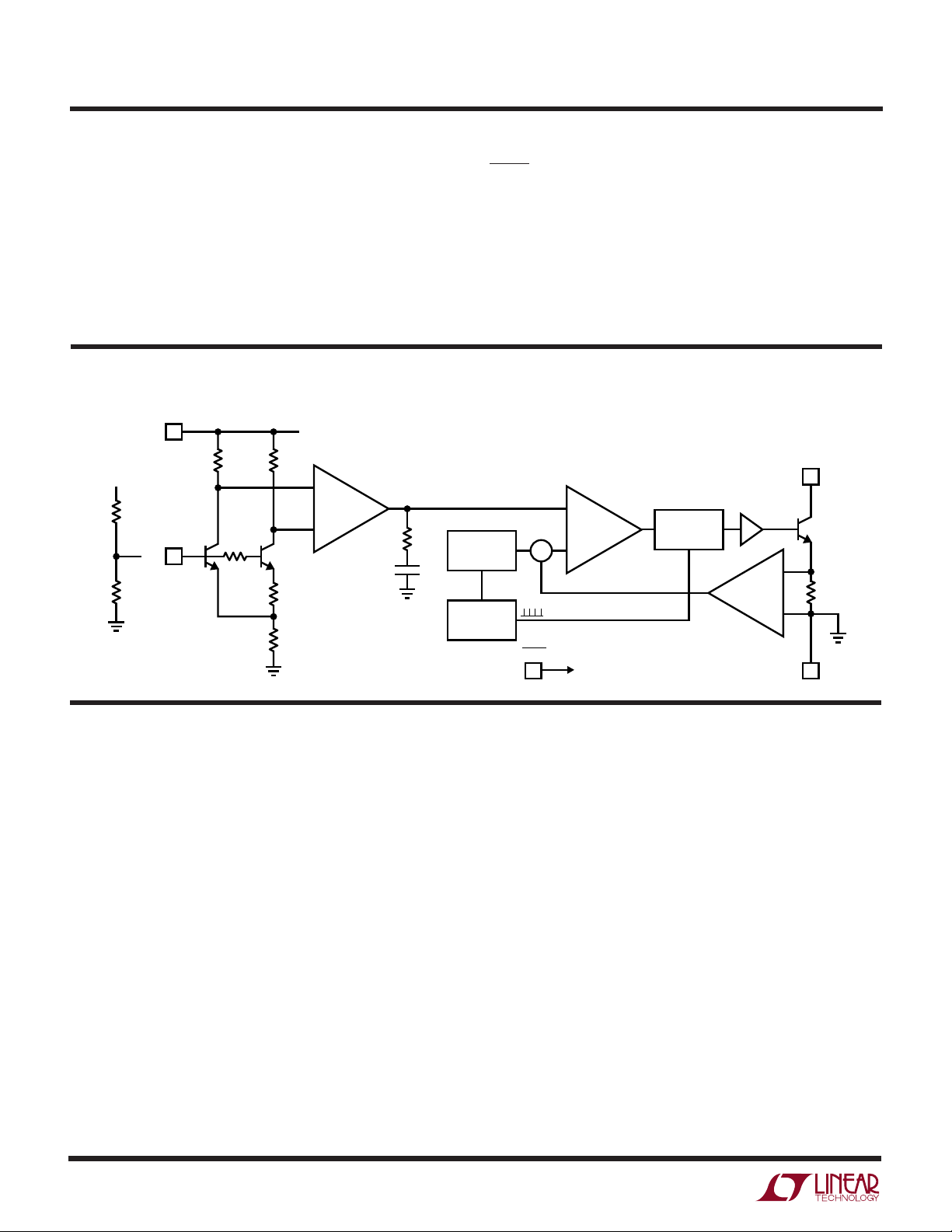
UUU
PIN FUNCTIONS
SW (Pin 1): Switch Pin. Connect inductor/diode here.
Minimize trace area at this pin to keep EMI down.
GND (Pin 2): Ground. Tie directly to local ground plane.
FB (Pin 3): Feedback Pin. Reference voltage is 1.23V.
Connect resistive divider tap here. Minimize trace area at
FB. Set V
according to V
OUT
= 1.23V(1 + R1/R2).
OUT
W
BLOCK DIAGRAM
Q2
x10
R6
40k
R3
30k
R4
140k
V
IN
+
A1
g
m
–
R
C
C
C
GENERATOR
1.4MHz
OSCILLATOR
V
OUT
R1
(EXTERNAL)
R2
(EXTERNAL)
V
5
IN
R5
40k
FB
Q1
3
FB
SHDN (Pin 4): Shutdown Pin. Tie to 1V or more to enable
device. Ground to shut down.
VIN (Pin 5): Input Supply Pin. Must be locally bypassed.
SW
1
Q3
+
0.15Ω
–
2
GND
1613 • BD
RAMP
SHDN
4
Σ
COMPARATOR
–
A2
+
SHUTDOWN
FF
RQ
S
DRIVER
U
OPERATIO
The LT1613 is a current mode, internally compensated,
fixed frequency step-up switching regulator. Operation
can be best understood by referring to the Block Diagram.
Q1 and Q2 form a bandgap reference core whose loop is
closed around the output of the regulator. The voltage
drop across R5 and R6 is low enough such that Q1 and Q2
do not saturate, even when VIN is 1V. When there is no
load, FB rises slightly above 1.23V, causing VC (the error
amplifier’s output) to decrease. Comparator A2’s output
stays high, keeping switch Q3 in the off state. As increased
output loading causes the FB voltage to decrease, A1’s
output increases. Switch current is regulated directly on a
cycle-by-cycle basis by the VC node. The flip flop is set at
the beginning of each switch cycle, turning on the switch.
When the summation of a signal representing switch
current and a ramp generator (introduced to avoid
subharmonic oscillations at duty factors greater than
50%) exceeds the VC signal, comparator A2 changes
state, resetting the flip flop and turning off the switch.
More power is delivered to the output as switch current is
increased. The output voltage, attenuated by external
resistor divider R1 and R2, appears at the FB pin, closing
the overall loop. Frequency compensation is provided
internally by RC and CC. Transient response can be optimized by the addition of a phase lead capacitor CPL in
parallel with R1 in applications where large value or low
ESR output capacitors are used.
As the load current is decreased, the switch turns on for a
shorter period each cycle. If the load current is further
decreased, the converter will skip cycles to maintain
output voltage regulation. If the FB pin voltage is increased
significantly above 1.23V, the LT1613 will enter a low
power state where quiescent current falls to approximately 100µA.
4
Page 5

OPERATIO
LT1613
U
LAYOUT
The LT1613 switches current at high speed, mandating
careful attention to layout for proper performance.
You
will not get advertised performance with careless layouts.
Figure 2 shows recommended component placement for
a boost (step-up) converter. Follow this closely in your
PCB layout. Note the direct path of the switching loops.
Input capacitor C1
must
be placed close (<5mm) to the IC
package. As little as 10mm of wire or PC trace from CIN to
VIN will cause problems such as inability to regulate or
oscillation.
The ground terminal of output capacitor C2 should tie
close to Pin 2 of the LT1613. Doing this reduces dI/dt in the
ground copper which keeps high frequency spikes to a
minimum. The DC/DC converter ground should tie to the
PC board ground plane at one place only, to avoid introducing dI/dt in the ground plane.
A SEPIC (single-ended primary inductance converter)
schematic is shown in Figure 3. This converter topology
produces a regulated output voltage that spans (i.e., can
be higher or lower than) the output. Recommended component placement for a SEPIC is shown in Figure 4.
L1A
V
IN
SHDN
22µH
LT1613
GND
V
IN
4V TO
7V
+
C1
15µF
C1, C2: AVX TAJA156M016
C3: TAIYO YUDEN JMK325BJ226MM
D1: MOTOROLA MBR0520
L1, L2: MURATA LQH3C220
C3
1µF
R2
32.4k
R1
100k
L1B
22µH
D1
V
OUT
5V/150mA
+
C2
15µF
1613 F03
SW
FBSHDN
Figure 3. Single-Ended Primary Inductance Converter (SEPIC)
Generates 5V from An Input Voltage Above or Below 5V
L1AL1B
+
V
OUT
D1
C3
+
C2
VIAS TO
GROUND
PLANE
R2
C1
15
2
34
V
IN
SHUTDOWN
L1
+
V
OUT
+
VIAS TO
GROUND
PLANE
D1
C2
R2
GROUND
C1
15
2
34
R1
V
IN
SHUTDOWN
1613 F02
Figure 2. Recommended Component Placement for Boost
Converter. Note Direct High Current Paths Using Wide PCB
Traces. Minimize Area at Pin 3 (FB). Use Vias to Tie Local
Ground Into System Ground Plane. Use Vias at Location Shown
to Avoid Introducing Switching Currents Into Ground Plane
GROUND
R1
1613 F04
Figure 4. Recommended Component Placement for SEPIC
COMPONENT SELECTION
Inductors
Inductors used with the LT1613 should have a saturation
current rating (where inductance is approximately 70% of
zero current inductance) of approximately 0.5A or greater.
DCR of the inductors should be 0.5Ω or less. For boost
converters, inductance should be 4.7µH for input voltage
less than 3.3V and 10µH for inputs above 3.3V. When
using the device as a SEPIC, either a coupled inductor or
two separate inductors can be used. If using separate
inductors, 22µH units are recommended for input voltage
above 3.3V. Coupled inductors have a beneficial mutual
inductance, so a 10µH coupled inductor results in the
same ripple current as two 20µH uncoupled units.
5
Page 6

LT1613
OPERATIO
U
Table 1 lists several inductors that will work with the
LT1613, although this is not an exhaustive list. There are
many magnetics vendors whose components are suitable
for use.
Diodes
A Schottky diode is recommended for use with the LT1613.
The Motorola MBR0520 is a very good choice. Where the
input to output voltage differential exceeds 20V, use the
MBR0530 (a 30V diode). If cost is more important than
efficiency, the 1N4148 can be used, but only at low current
loads.
Capacitors
The input bypass capacitor must be placed physically
close to the input pin. ESR is not critical and in most cases
an inexpensive tantalum is appropriate.
The choice of output capacitor is far more important. The
quality of this capacitor is the greatest determinant of the
output voltage ripple. The output capacitor must have
enough capacitance to satisfy the load under transient
conditions and it must shunt the switched component of
current coming through the diode. Output voltage ripple
results when this switched current passes through the
finite output impedance of the output capacitor. The
capacitor should have low impedance at the 1.4MHz
switching frequency of the LT1613. At this frequency, the
impedance is usually dominated by the capacitor’s equivalent series resistance (ESR). Choosing a capacitor with
lower ESR will result in lower output ripple.
Ceramic capacitors can be used with the LT1613 provided
loop stability is considered. A tantalum capacitor has
some ESR and this causes an “ESR zero” in the regulator
loop. This zero is beneficial to loop stability. The internally
compensated LT1613 does not have an accessible compensation node, but other circuit techniques can be employed to counteract the loss of the ESR zero, as detailed
in the next section.
Some capacitor types appropriate for use with the LT1613
are listed in Table 2.
OPERATION WITH CERAMIC CAPACITORS
Because the LT1613 is internally compensated, loop stability must be carefully considered when choosing an
output capacitor. Small, low cost tantalum capacitors
have some ESR, which aids stability. However, ceramic
capacitors are becoming more popular, having attractive
characteristics such as near-zero ESR, small size and
reasonable cost. Simply replacing a tantalum output capacitor with a ceramic unit will decrease the phase margin,
in some cases to unacceptable levels. With the addition of
a phase lead capacitor (CPL) and isolating resistor (R3),
the LT1613 can be used successfully with ceramic output
capacitors as described in the following figures.
A boost converter, stepping up 2.5V to 5V, is shown in
Figure 5. Tantalum capacitors are used for the input and
output (the input capacitor is not critical and has little
6
Table 1. Inductor Vendors
VENDOR PHONE URL PART COMMENT
Sumida (847) 956-0666 www.sumida.com CLS62-22022 22µH Coupled
CD43-220 22µH
Murata (404) 436-1300 www.murata.com LQH3C-220 22µH, 2mm Height
LQH3C-100 10µH
LQH3C-4R7 4.7µH
Coiltronics (407) 241-7876 www.coiltronics.com CTX20-1 20µH Coupled, Low DCR
Table 2. Capacitor Vendors
VENDOR PHONE URL PART COMMENT
Taiyo Yuden (408) 573-4150 www.t-yuden.com Ceramic Caps X5R Dielectric
AVX (803) 448-9411 www.avxcorp.com Ceramic Caps
Tantalum Caps
Murata (404) 436-1300 www.murata.com Ceramic Caps
Page 7

OPERATIO
V
IN
V
OUT
5V
C
PL
330pF
1613 F08
SW
L1
10µH
D1
GND
LT1613
C1: AVX TAJA156M010R
C2: TAIYO YUDEN LMK325BJ106MN
D1: MBR0520
L1: MURATA LQH3C100K04
R2
12.1k
R3
10k
R1
37.4k
FBSHUTDOWN
C1
15µF
V
IN
2.5V
C2
10µF
SHDN
+
LT1613
U
effect on loop stability, as long as minimum capacitance
requirements are met). The transient response to a load
step of 50mA to 100mA is pictured in Figure 6. Note the
“double trace,” due to the ESR of C2. The loop is stable and
settles in less than 100µs. In Figure 7, C2 is replaced by a
10µF ceramic unit. Phase margin decreases drastically,
L1
V
IN
SHDN
10µH
LT1613
GND
V
IN
2.5V
+
C1
15µF
C1: AVX TAJA156M010R
C2: AVX TAJA226M006R
D1: MOTOROLA MBR0520
L1: MURATA LQH3C100
Figure 5. 2.5V to 5V Boost Converter with “A”
Case Size Tantalum Input and Output Capacitors
SW
D1
R1
37.4k
FBSHDN
R2
12.1k
V
OUT
5V
+
C2
22µF
1613 F05
resulting in a severely underdamped response. By adding
R3 and CPL as detailed in Figure 8’s schematic, phase
margin is restored, and transient response to the same
load step is pictured in Figure 9. R3 isolates the device FB
pin from fast edges on the V
node due to parasitic PC
OUT
trace inductance.
Figure 10’s circuit details a 5V to 12V boost converter,
delivering up to 130mA. The transient response to a load
step of 10mA to 130mA, without CPL, is pictured in
Figure 11. Although the ringing is less than that of the
previous example, the response is still underdamped and
can be improved. After adding R3 and CPL, the improved
transient response is detailed in Figure 12.
Figure 13 shows a SEPIC design, converting a 3V to 10V
input to a 5V output. The transient response to a load step
of 20mA to 120mA, without CPL and R3, is pictured in
Figure 14. After adding these two components, the improved response is shown in Figure 15.
V
OUT
20mV/DIV
AC COUPLED
LOAD CURRENT
100mA
50mA
200µs/DIV
1613 F06
Figure 6. 2.5V to 5V Boost Converter Transient
Response with 22µF Tantalum Output Capacitor.
Apparent Double Trace on V
Is Due to Switching
OUT
Frequency Ripple Current Across Capacitor ESR
V
OUT
20mV/DIV
AC COUPLED
LOAD CURRENT
100mA
50mA
Figure 7. 2.5V to 5V Boost Converter with
10µF Ceramic Output Capacitor, No C
200µs/DIV
1613 F07
PL
Figure 8. 2.5V to 5V Boost Converter with Ceramic
Output Capacitor. CPL Added to Increase Phase Margin,
R3 Isolates FB Pin from Fast Edges
V
OUT
20mV/DIV
AC COUPLED
LOAD CURRENT
100mA
50mA
200µs/DIV
Figure 9. 2.5V to 5V Boost Converter with 10µF Ceramic
Output Capacitor, 330pF CPL and 10k in Series with FB Pin
1613 F09
7
Page 8

LT1613
OPERATIO
U
V
IN
SHDN
10µH
LT1613
GND
V
IN
5V
+
C1
22µF
C1: AVX TAJB226M010
C2: TAIYO YUDEN EMK325BJ475MN
D1: MOTOROLA MBR0520
L1: MURATA LQH3C100
L1
SW
D1
C
PL
200pF
R1
R3
107k
10k
FBSHUTDOWN
R2
12.3k
Figure 10. 5V to 12V Boost Converter with 4.7µF Ceramic
Output Capacitor, CPL Added to Increase Phase Margin
V
OUT
100mV/DIV
AC COUPLED
V
OUT
12V
130mA
C2
4.7µF
1613 F10
V
IN
3V TO
10V
+
C1
22µF
C1: AVX TAJB226M010
C2: TAIYO YUDEN LMK325BJ106MN
C3: TAIYO YUDEN LMK212BJ105MG
D1: MOTOROLA MBR0520
L1, L2: MURATA LQH3C220
V
IN
SHDN
Figure 13. 5V Output SEPIC with Ceramic
Output Capacitor. CPL Adds Phase Margin
V
OUT
50mV/DIV
AC COUPLED
L1
22µH
LT1613
GND
SW
C3
1µF
L2
C
22µH
R3
10k
FBSHUTDOWN
R2
12.1k
PL
330pF
R1
37.4k
D1
V
5V
C2
10µF
1613 F13
OUT
LOAD CURRENT
AC COUPLED
LOAD CURRENT
Figure 12. 5V to 12V Boost Converter with 4.7µF
Ceramic Output Capacitor and 200pF Phase-Lead
Capacitor CPL and 10k in Series with FB Pin
130mA
10mA
200µs/DIV
Figure 11. 5V to 12V Boost Converter
with 4.7µF Ceramic Output Capacitor
V
OUT
100mV/DIV
130mA
10mA
200µs/DIV
1613 F11
1613 F12
LOAD CURRENT
120mA
20mA
200µs/DIV
Figure 14. 5V Output SEPIC with 10µF
Ceramic Output Capacitor. No CPL. VIN = 4V
V
OUT
50mV/DIV
AC COUPLED
LOAD CURRENT
120mA
20mA
200µs/DIV
Figure 15. 5V Output SEPIC with 10µF Ceramic Output
Capacitor, 330pF CPL and 10k in Series with FB Pin
1613 F14
1613 F15
8
Page 9

OPERATIO
LT1613
U
START-UP/SOFT-START
When the LT1613 SHDN pin voltage goes high, the device
rapidly increases the switch current until internal current
limit is reached. Input current stays at this level until the
output capacitor is charged to final output voltage. Switch
current can exceed 1A. Figure 16’s oscillograph details
start-up waveforms of Figure 17’s SEPIC into a 50Ω load
without any soft-start. The output voltage reaches final
value in approximately 200µs, while input current reaches
400mA. Switch current in a SEPIC is 2x the input current,
so the switch is conducting approximately 800mA peak.
Soft-start reduces the inrush current by taking more time
to reach final output voltage. A soft-start circuit consisting
of Q1, RS1, RS2 and CS1 as shown in Figure 17 can be used
to limit inrush current to a lower value. Figure 18 pictures
V
and input current with RS2 of 33kΩ and CS of 10nF.
OUT
Input current is limited to a peak value of 200mA as the
V
OUT
2V/DIV
time required to reach final value increases to 1.7ms. In
Figure 19, CS is increased to 33nF. Input current does not
exceed the steady-state current the device uses to supply
power to the 50Ω load. Start-up time increases to 4.3ms.
CS can be increased further for an even slower ramp, if
desired.
V
OUT
2V/DIV
I
IN
200mA/DIV
V
S
5V/DIV
500µs/DIV
Figure 18. Soft-Start Components in Figure 17’s SEPIC
Reduces Inrush Current. CSS = 10nF, R
V
OUT
2V/DIV
LOAD
1613 F18
= 50Ω
I
200mA/DIV
V
SHDN
5V/DIV
IN
200µs/DIV
Figure 16. Start-Up Waveforms of
Figure 17’s SEPIC Into 50Ω Load
SOFT-START COMPONENTS
R
S1
33k
S
C
S
R
10nF/
33nF
C1: AVX TAJB226M006
C2: TAIYO YUDEN LMK325BJ106MN
C3: TAIYO YUDEN LMK212BJ105MG
33k
S2
I
IN
200mA/DIV
V
S
1613 F16
5V/DIV
Figure 19. Increasing CS to 33nF Further
Reduces Inrush Current. R
SW
C3
1µF
L2
22µH
R3
10k
FBV
R2
12.1k
C
330pF
37.4k
L1
V
IN
4V
22µF
Q1
2N3904
+
C1
22µH
V
IN
LT1613
SHDN
GND
D1: MOTOROLA MBR0520
L1, L2: MURATA LQH3C220
Figure 17. 5V SEPIC with Soft-Start Components
1ms/DIV
= 50Ω
LOAD
PL
R1
D1
C2
10µF
R
LOAD
1613 F17
V
OUT
5V
1613 F18
9
Page 10

LT1613
U
TYPICAL APPLICATIO S
6.5V TO 4V
4-Cell to 5V SEPIC DC/DC Converter
L1
22µH
+
4-CELL
C1
15µF
V
IN
SHDN
SW
LT1613
FBSHDN
GND
1µF
C3
374k
121k
L2
22µH
D1
V
OUT
5V
175mA
+
C2
22µF
V
IN
3.5V TO
8V
+
C1
22µF
C1: AVX TAJB226M016
C2: AVX TAJA475M025
D1: MOTOROLA MBR0520
L1: MURATA LQH3C100
3.3V to 8V/70mA, –8V/5mA, 24V/5mA TFT LCD Bias Supply Uses All Ceramic Capacitors
V
IN
SHDN
L1, L2: MURATA LQH3C220
C3: AVX 1206YG105 CERAMIC
D1: MBR0520
L1
10µH
LT1613
GND
SW
D1
1nF
10k
FBSHDN
4-Cell to 15V/30mA DC/DC Converter
V
OUT
R1
137k
1%
R2
12.1k
+
0.22µF
15V/30mA
C2
4.7µF
D2
1613 TA04
0.22µF
1µF
85
80
75
70
65
EFFICIENCY (%)
60
55
50
1613 • TA03
Efficiency
VIN = 6.5V
VIN = 3.6V
0 102030405060708090100
D3
LOAD CURRENT (mA)
V
OFF
–8V
5mA
V
ON
24V
5mA
1µF
VIN = 5V
1613 TA04a
10
0.22µF: TAIYO YUDEN EMK212BJ224MG
1µF: TAIYO YUDEN LMK212BJ105MG
4.7µF: TAIYO YUDEN LMK316BJ475ML
D1: MOTOROLA MBRO520
D2, D3, D4: BAT54S
L1: SUMIDA CDRH5D185R4
V
3.3V
IN
C1
4.7µF
5.4µH
V
IN
LT1613
GND
D4
0.22µF
L1
D1
SW
274k
FBSHDN
48.7k
1µF
C2
4.7µF
1613 TA05
AV
8V
70mA
DD
Page 11

U
TYPICAL APPLICATIO S
4-Cell to 5V/50mA, 12V/10mA, 15V/10mA Digital Camera Power Supply
C1: TAIYO YUDEN JMK316BJ106ML
C2, C3, C4: TAIYO YUDEN EMK212BJ105MG
C5: TAIYO YUDEN JMK212BJ475MG
D1: MOTOROLA MBR0520
D2, D3: BAT54
T1: COILCRAFT CCI8245A (847) 639-6400
7V TO 3.6V
V
IN
C1
10µF
LT1613
D3
2
D2
5
T1
6
1
V
IN
SW
D1
3
4
C2
1µF
C3
1µF
C4
1µF
C5
4.7µF
270pF
15V/10mA
12V/10mA
5V/50mA
SHUTDOWN
LT1613
FBSHDN
GND
102k
33.2k
4-Cell to 5V/50mA, 15V/10mA, –7.5V/10mA Digital Camera Power Supply
D2
C1: TAIYO YUDEN JMK316BJ106ML
C2, C3, C4: TAIYO YUDEN EMK212BJ105MG
C5: TAIYO YUDEN JMK212BJ475MG
D1: MOTOROLA MBR0520
D2, D3: BAT54
T1: COILCRAFT CCI8244A (847) 639-6400
V
7V TO 3.6V
IN
C1
10µF
V
IN
2
D1
5
T1
3
6
1
SW
4
C2
1µF
D3
270pF
C3
1µF
C5
4.7µF
C4
1µF
1613 TA07
15V/10mA
5V/50mA
–7.5V/10mA
LT1613
SHUTDOWN
Information furnished by Linear Technology Corporation is believed to be accurate and reliable.
However, no responsibility is assumed for its use. Linear Technology Corporation makes no representation that the interconnection of its circuits as described herein will not infringe on existing patent rights.
FBSHDN
GND
102k
33.2k
1613 TA08
11
Page 12

LT1613
U
TYPICAL APPLICATIONS
V
IN
2.7V
TO 4.5V
+
C1: AVX TAJA4R7M010
C2: TAIYO YUDEN LMK212BJ105MG
D1: BAT54S DUAL DIODE
L1: MURATA LQH3C2R2
PACKAGE DESCRIPTION
2.60 – 3.00
(0.102 – 0.118)
1.50 – 1.75
(0.059 – 0.069)
Li-Ion to 16V/20mA Step-Up DC/DC Converter
C1
4.7µF
V
IN
SHDN
L1
2.2µH
SW
LT1613
FBSHDN
GND
D1
165k
1%
13.7k
1%
C2
1µF
X5R
CERAMIC
1613 TA06
16V
20mA
U
Dimensions in inches (millimeters) unless otherwise noted.
S5 Package
5-Lead Plastic SOT-23
(LTC DWG # 05-08-1633)
2.80 – 3.00
0.00 – 0.15
(0.00 – 0.006)
0.90 – 1.45
(0.035 – 0.057)
(0.110 – 0.118)
(NOTE 3)
0.35 – 0.55
(0.014 – 0.022)
NOTE:
1. DIMENSIONS ARE IN MILLIMETERS
2. DIMENSIONS ARE INCLUSIVE OF PLATING
3. DIMENSIONS ARE EXCLUSIVE OF MOLD FLASH AND METAL BURR
4. MOLD FLASH SHALL NOT EXCEED 0.254mm
5. PACKAGE EIAJ REFERENCE IS SC-74A (EIAJ)
0.09 – 0.20
(0.004 – 0.008)
(NOTE 2)
0.35 – 0.50
(0.014 – 0.020)
FIVE PLACES (NOTE 2)
0.90 – 1.30
(0.035 – 0.051)
1.90
(0.074)
REF
0.95
(0.037)
REF
S5 SOT-23 0599
RELATED PARTS
PART NUMBER DESCRIPTION COMMENTS
LT1307 Single Cell Micropower DC/DC 3.3V/75mA From 1V; 600kHz Fixed Frequency
LT1317 2-Cell Micropower DC/DC 3.3V/200mA From Two Cells; 600kHz Fixed Frequency
LTC1474 Low Quiescent Current, High Efficiency Step-Down Converter 94% Efficiency, 10µA IQ, 9V to 5V at 250µA
LT1521 300mA Low Dropout Regulator with Micropower Quiescent 500mV Dropout, 300mA Output Current, 12µA I
Current and Shutdown
LTC1517-5 Micropower, Regulated Charge Pump 3-Cells to 5V at 20mA, SOT-23 Package, 6µA I
LT1610 1.7MHz Single Cell Micropower DC/DC Converter 30µA IQ, MSOP Package, Internal Compensation
LT1611 Inverting 1.4MHz Switching Regulator 5V to –5V at 150mA, Low Output Noise
LT1615/LT1615-1 Micropower DC/DC Converter in 5-Lead SOT-23 20V at 12mA from 2.5V Input, Tiny SOT-23 Package
Q
Q
12
Linear Technology Corporation
1630 McCarthy Blvd., Milpitas, CA 95035-7417
(408) 432-1900 ● FAX: (408) 434-0507
●
www.linear-tech.com
1613f LT/TP 1299 4K • PRINTED IN USA
LINEAR TE CHNOLOGY CORPOR ATION 1997
 Loading...