

Page 1
FEATURES
■
Uses Tiny Capacitors and Inductor
■
Internally Compensated
■
Low Quiescent Current: 30µA
■
Operates with VIN as Low as 1V
■
3V at 30mA from a Single Cell
■
5V at 200mA from 3.3V
■
High Output Voltage Capability: Up to 28V
■
Low Shutdown Current: <1µA
■
Automatic Burst ModeTM Switching at Light Load
■
Low V
■
8-Lead MSOP and SO Packages
Switch: 300mV at 300mA
CESAT
U
APPLICATIO S
LT1610
1.7MHz, Single Cell
Micropower
DC/DC Converter
U
DESCRIPTIO
The LT®1610 is a micropower fixed frequency DC/DC
converter that operates from an input voltage as low as 1V.
Intended for small, low power applications, it switches at
1.7MHz, allowing the use of tiny capacitors and inductors.
The device can generate 3V at 30mA from a single cell
(1V) supply. An internal compensation network can be
connected to the LT1610’s VC pin, eliminating two external components. No-load quiescent current of the LT1610
is 30µA, and the internal NPN power switch handles a
300mA current with a voltage drop of 300mV.
The LT1610 is available in 8-lead MSOP and SO packages.
■
Pagers
■
Cordless Phones
■
Battery Backup
■
LCD Bias
■
Portable Electronic Equipment
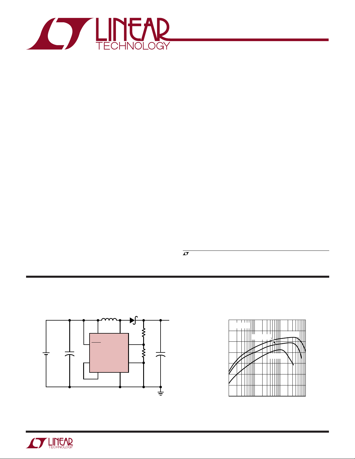
TYPICAL APPLICATIO
L1
4.7µH
65
V
IN
3
C1
22µF
SHDN
LT1610
8
V
C
1
+
1 CELL
C1, C2: AVX TAJA226M006R
D1: MOTOROLA MBR0520
L1: MURATA LQH1C4R7
Figure 1. 1-Cell to 3V Step-Up Converter
U
SW
GNDCOMP
PGND
, LTC and LT are registered trademarks of Linear Technology Corporation.
Burst Mode is a trademark of Linear Technology Corporation.
D1
R1
1M
2
FB
R2
681k
7
4
V
OUT
3V
30mA
+
C2
22µF
1610 F01
85
V
OUT
80
75
70
65
EFFICIENCY (%)
60
55
50
0.1
Efficiency
= 3V
VIN = 1.25V
VIN = 1V
1 10 100
LOAD CURRENT (mA)
VIN = 1.5V
1610 TA01
1
Page 2
LT1610
1
2
3
4
8
7
6
5
TOP VIEW
V
C
FB
SHDN
PGND
COMP
GND
V
IN
SW
S8 PACKAGE
8-LEAD PLASTIC SO
WW
W
U
ABSOLUTE MAXIMUM RATINGS
(Note 1)
VIN Voltage ................................................................ 8V
SW Voltage ............................................... –0.4V to 30V
FB Voltage ..................................................... VIN + 0.3V
VC Voltage ................................................................ 2V
COMP Voltage .......................................................... 2V
Current into FB Pin .............................................. ±1mA
SHDN Voltage ............................................................ 8V
U
W
U
PACKAGE/ORDER INFORMATION
ORDER PART
TOP VIEW
V
1
C
2
FB
3
SHDN
4
PGND
MS8 PACKAGE
8-LEAD PLASTIC MSOP
T
= 125°C, θJA = 160°C/W
JMAX
8
7
6
5
COMP
GND
V
IN
SW
NUMBER
LT1610CMS8
MS8 PART MARKING
LTDT
Maximum Junction Temperature ......................... 125°C
Operating Temperature Range (Note 1)
Commercial .............................................0°C to 70°C
Extended Commercial (Note 2).......... –40°C to 85°C
Industrial ........................................... –40°C to 85°C
Storage Temperature Range ................. –65°C to 150°C
Lead Temperature (Soldering, 10 sec).................. 300°C
ORDER PART
NUMBER
LT1610CS8
LT1610IS8
S8 PART MARKING
1610
T
= 125°C, θJA = 120°C/W
JMAX
1610I
Consult factory for Military grade parts.
LECTRICAL C CHARA TERIST
E
range, otherwise specifications are at T
= 25°C. Commercial grade 0°C to 70°C, V
A
ICS
The ● denotes specifications which apply over the specified temperature
= 1.5V, V
IN
= VIN, unless otherwise noted.
SHDN
(Note 2)
PARAMETER CONDITIONS MIN TYP MAX UNITS
Minimum Operating Voltage 0.9 1 V
Maximum Operating Voltage 8V
Feedback Voltage ● 1.20 1.23 1.26 V
Quiescent Current V
Quiescent Current in Shutdown V
FB Pin Bias Current ● 27 80 nA
Reference Line Regulation 1V ≤ VIN ≤ 2V (25°C, 0°C) 0.6 1 %/V
Error Amp Transconductance ∆I = 2µA25µmhos
Error Amp Voltage Gain 100 V/V
Switching Frequency ● 1.4 1.7 2 MHz
Maximum Duty Cycle 77 80 95 %
= 1.5V, Not Switching 30 60 µA
SHDN
= 0V, VIN = 2V 0.01 0.5 µA
SHDN
= 0V, VIN = 5V 0.01 1.0 µA
V
SHDN
≤ 2V (70°C) 2 %/V
1V ≤ V
IN
2V ≤ V
≤ 8V (25°C, 0°C) 0.03 0.15 %/V
IN
≤ 8V (70°C) 0.2 %/V
2V ≤ V
IN
● 75 95 %
2
Page 3
LT1610
LECTRICAL C CHARA TERIST
E
range, otherwise specifications are at T
= 25°C. Commercial grade 0°C to 70°C, V
A
ICS
The ● denotes specifications which apply over the specified temperature
= 1.5V, V
IN
= VIN, unless otherwise noted.
SHDN
(Note 2)
PARAMETER CONDITIONS MIN TYP MAX UNITS
Switch Current Limit (Note 3) 450 600 900 mA
Switch V
CESAT
Switch Leakage Current VSW = 5V 0.01 1 µA
SHDN Input Voltage High 1V
SHDN Input Voltage Low 0.3 V
SHDN Pin Bias Current V
ISW = 300mA 300 350 mV
● 400 mV
= 3V 10 µA
SHDN
= 0V 0.01 0.1 µA
V
SHDN
The ● denotes specifications which apply over the specified temperature range, otherwise specifications are at TA = 25°C.
Industrial grade –40°C to 85°C, V
PARAMETER CONDITIONS MIN TYP MAX UNITS
Minimum Operating Voltage TA = 85°C 0.9 1 V
Maximum Operating Voltage 8V
Feedback Voltage ● 1.20 1.23 1.26 V
Quiescent Current 30 60 µA
Quiescent Current in Shutdown V
FB Pin Bias Current ● 27 80 nA
Reference Line Regulation 2V ≤ VIN ≤ 8V (–40°C) 0.03 0.15 %/V
Error Amp Transconductance ∆I = 2µA25µmhos
Error Amp Voltage Gain 100 V/V
Switching Frequency (Note 4) ● 1.4 1.7 2 MHz
Maximum Duty Cycle (Note 4) 77 80 95 %
Switch Current Limit 450 600 900 mA
Switch V
CESAT
Switch Leakage Current VSW = 5V 0.01 1 µA
SHDN Input Voltage High 1V
SHDN Input Voltage Low 0.3 V
SHDN Pin Bias Current V
= 1.5V, V
IN
= VIN, unless otherwise noted.
SHDN
= –40°C 1.25 V
T
A
= 0V, VIN = 2V 0.01 0.5 µA
SHDN
= 0V, VIN = 5V 0.01 1.0 µA
V
SHDN
≤ 8V (85°C) 0.2 %/V
2V ≤ V
IN
● 75 95 %
ISW = 300mA 300 350 mV
● 400 mV
= 3V 10 µA
SHDN
V
= 0V 0.01 0.1 µA
SHDN
Note 1: Absolute Maximum Ratings are those values beyond which the life
of a device may be impaired.
Note 2: The LT1610C is guaranteed to meet specified performance from
0°C to 70°C and is designed, characterized and expected to meet these
extended temperature limits, but is not tested at –40°C and 85°C. The
LT1610I is guaranteed to meet the extended temperature limits.
Note 3: Current limit guaranteed by design and/or correlation to static test.
Current limit is affected by duty cycle due to ramp generator. See Block
Diagram.
Note 4: Not 100% tested at 85°C.
3
Page 4

LT1610
UW
TYPICAL PERFOR A CE CHARACTERISTICS
Current Limit (DC = 30%)
600
500
400
(mV)
CESAT
300
V
200
100
CESAT
0
vs Current
TA = 25°C
200 300 400
100
SWITCH CURRENT (mA)
TA = 85°C
= –40°C
T
A
500 600
1610 G01
vs Temperature
800
700
600
500
400
SWITCH CURRENT LIMIT (mA)
300
200
–50
02550
–25
TEMPERATURE (°C)
75 100
1610 G02
Current Limit vs Duty CycleV
800
700
600
500
400
300
CURRENT LIMIT (mA)
200
100
0
20 40 60 1007010 30 50 90
0
TA = 25°C
80
DUTY CYCLE (%)
1610 G03
Oscillator Frequency
vs Input Voltage Feedback Voltage
2.50
TA = 25°C
2.25
2.00
1.75
1.50
1.25
1.00
0.75
0.50
SWITCHING FREQUENCY (MHz)
0.25
0
0
13
2
INPUT VOLTAGE (V)
SHDN Pin Current
vs SHDN Pin Voltage
50
40
30
20
SHDN CURRENT (µA)
10
7
4
6
5
1610 G04
1.240
1.235
1.230
1.225
1.220
FEEDBACK VOLTAGE (V)
1.215
1.210
8
V
OUT
50mV/DIV
AC COUPLED
100mA/DIV
31mA
I
LOAD
1mA
–50
–25
Transient Response,
Circuit of Figure 1
I
L1
VIN = 1.25V 500µs/DIV
V
= 3V
OUT
02550
TEMPERATURE (°C)
75 100
1610 G05
1610 TA08
40
35
30
25
20
15
10
QUIESCENT CURRENT (µA)
V
OUT
20mV/DIV
AC COUPLED
SWITCH
VOLTAGE
2V/DIV
SWITCH
CURRENT
50mA/DIV
Quiescent Current
vs Temperature
5
0
–25 0 50
–50
25
TEMPERATURE (°C)
Burst Mode Operation,
Circuit of Figure 1
= 1.25V 20µs/DIV
V
IN
= 3V
V
OUT
= 3mA
I
LOAD
75
100
1610 G06
1610 TA08
4
0
0
12
SHDN VOLTAGE (V)
4
35 8
67
1610 G07
Page 5
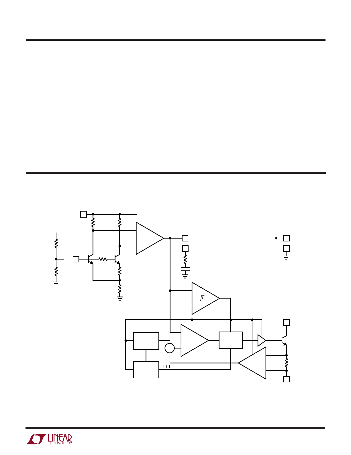
UUU
PIN FUNCTIONS
LT1610
VC (Pin 1): Error Amplifier Output. Frequency compensation network must be connected to this pin, either internal
(COMP pin) or external series RC to ground. 220kΩ/
220pF typical value.
FB (Pin 2): Feedback Pin. Reference voltage is 1.23V.
Connect resistive divider tap here. Minimize trace area at
FB. Set V
according to V
OUT
= 1.23V (1 + R1/R2).
OUT
SHDN (Pin 3): Shutdown. Ground this pin to turn off
device. Tie to 1V or more to enable.
PGND (Pin 4): Power Ground. Tie directly to local ground
plane.
W
BLOCK DIAGRA
V
IN
V
OUT
R1
(EXTERNAL)
R2
(EXTERNAL)
6
R5
40k
Q1
FB
2
FB
Q2
× 10
R6
40k
R3
30k
V
IN
+
A1
g
m
–
SW (Pin 5): Switch Pin. Connect inductor/diode here.
Minimize trace area at this pin to keep EMI down.
VIN (Pin 6): Input Supply Pin. Must be locally bypassed.
GND (Pin 7): Signal Ground. Carries all device ground
current except switch current. Tie to local ground plane.
COMP (Pin 8): Internal Compensation Network. Tie to V
C
pin, or let float if external compensation is used. Output
capacitor must be tantalum if COMP pin is used for compensation.
1
V
C
COMP
8
R
C
C
C
3
SHDNSHUTDOWN
GND
7
R4
140k
+
BIAS
RAMP
GENERATOR
Σ
1.7MHz
OSCILLATOR
–
A2
+
–
COMPARATOR
Figure 2. LT1610 Block Diagram
ENABLE
FF
RQ
S
A = 3
DRIVER
+
–
5
Q3
4
SW
0.15Ω
PGND
1610 F02
5
Page 6

LT1610
U
WUU
APPLICATIONS INFORMATION
OPERATION
The LT1610 combines a current mode, fixed frequency
PWM architecture with Burst Mode micropower operation
to maintain high efficiency at light loads. Operation can be
best understood by referring to the block diagram in
Figure 2. Q1 and Q2 form a bandgap reference core whose
loop is closed around the output of the converter. When
VIN is 1V, the feedback voltage of 1.23V, along with an
70mV drop across R5 and R6, forward biases Q1 and Q2’s
base collector junctions to 300mV. Because this is not
enough to saturate either transistor, FB can be at a higher
voltage than VIN. When there is no load, FB rises slightly
above 1.23V, causing VC (the error amplifier’s output) to
decrease. When VC reaches the bias voltage on hysteretic
comparator A1, A1’s output goes low, turning off all
circuitry except the input stage, error amplifier and lowbattery detector. Total current consumption in this state is
30µA. As output loading causes the FB voltage to de-
crease, A1’s output goes high, enabling the rest of the IC.
Switch current is limited to approximately 100mA initially
after A1’s output goes high. If the load is light, the output
voltage (and FB voltage) will increase until A1’s output
goes low, turning off the rest of the LT1610. Low frequency ripple voltage appears at the output. The ripple
frequency is dependent on load current and output capacitance. This Burst Mode operation keeps the output regulated and reduces average current into the IC, resulting in
high efficiency even at load currents of 1mA or less.
If the output load increases sufficiently, A1’s output remains
high, resulting in continuous operation. When the LT1610
is running continuously, peak switch current is controlled
by VC to regulate the output voltage. The switch is turned
on at the beginning of each switch cycle. When the summation of a signal representing switch current and a ramp
generator (introduced to avoid subharmonic oscillations at
duty factors greater than 50%) exceeds the VC signal,
comparator A2 changes state, resetting the flip-flop and
turning off the switch. Output voltage increases as switch
current is increased. The output, attenuated by a resistor
divider, appears at the FB pin, closing the overall loop.
Frequency compensation is provided by either an external
series RC network connected between the VC pin and
ground or the internal RC network on the COMP pin (Pin
8). The typical values for the internal RC are 50k and 50pF.
LAYOUT
Although the LT1610 is a relatively low current device, its
high switching speed mandates careful attention to layout
for optimum performance. For boost converters, follow
the component placement indicated in Figure 3 for the best
results. C2’s negative terminal should be placed close to
Pin 4 of the LT1610. Doing this reduces switching currents
in the ground copper which keeps high frequency “spike”
noise to a minimum. Tie the local ground into the system
ground plane at one point only, using a few vias, to avoid
introducing dI/dt induced noise into the ground plane.
6
GROUND PLANE
R1
SHUTDOWN
MULTIPLE
VIAs
Figure 3. Recommended Component Placement for Boost Converter. Note Direct High Current Paths Using
Wide PC Traces. Minimize Trace Area at Pin 1 (VC) and Pin 2 (FB). Use Multiple Vias to Tie Pin 4 Copper to
Ground Plane. Use Vias at One Location Only to Avoid Introducing Switching Currents into the Ground Plane
R2
GND
1
2
LT1610
3
4
+
C2
8
C1
7
6
5
D1
V
OUT
V
IN
+
L1
1610 F03
Page 7

LT1610
U
WUU
APPLICATIONS INFORMATION
A SEPIC (Single-Ended Primary Inductance Converter)
schematic is shown in Figure 4. This converter topology
produces a regulated output over an input voltage range
L1
INPUT
Li-ION
3V to 4.2V
+
C1
22µF
6.3V
C1, C2: AVX TAJA226M006
C3: AVX 1206YC105 (X7R)
D1: MOTOROLA MBR0520
L1, L2: MURATA LQH3C220 (UNCOUPLED)
OR SUMIDA CLS62-220 (COUPLED)
1
8
22µH
65
V
IN
V
C
LT1610
COMP
GND
7
that spans (i.e., can be higher or lower than) the output.
Recommended component placement for a SEPIC is
shown in Figure 5.
C3
1µF
•
SW
SHDN
PGND
CERAMIC
2
FB
3
4
SHUTDOWN
1M
604k
•
L2
22µH
D1
V
OUT
3.3V
120mA
+
C2
22µF
6.3V
1610 F04
GROUND PLANE
R1
R2
SHUTDOWN
MULTIPLE
VIAs
Figure 4. Li-Ion to 3.3V SEPIC DC/DC Converter
V
IN
1
2
LT1610
3
4
C2
8
C1
7
6
5
+
L1 L2
C3
+
GND
D1
V
OUT
1610 F05
Figure 5. Recommended Component Placement for SEPIC
7
Page 8

LT1610
U
WUU
APPLICATIONS INFORMATION
COMPONENT SELECTION
Inductors
Inductors used with the LT1610 should have a saturation
current rating (–30% of zero current inductance) of approximately 0.5A or greater. DCR should be 0.5Ω or less.
The value of the inductor should be matched to the power
requirements and operating voltages of the application. In
most cases a value of 4.7µH or 10µH is suitable. The Murata
LQH3C inductors specified throughout the data sheet are
small and inexpensive, and are a good fit for the LT1610.
Alternatives are the CD43 series from Sumida and the
DO1608 series from Coilcraft. These inductors are slightly
larger but will result in slightly higher circuit efficiency.
Chip inductors, although tempting to use because of their
small size and low cost, generally do not have enough
energy storage capacity or low enough DCR to be used
successfully with the LT1610.
Diodes
The Motorola MBR0520 is a 0.5 amp, 20V Schottky diode.
This is a good choice for nearly any LT1610 application,
unless the output voltage or the circuit topology require a
diode rated for higher reverse voltages. Motorola also
offers the MBR0530 (30V) and MBR0540 (40V) versions.
Most one-half amp and one amp Schottky diodes are
suitable; these are available from many manufacturers. If
you use a silicon diode, it must be an ultrafast recovery
type. Efficiency will be lower due to the silicon diode’s
higher forward voltage drop.
Capacitors
impedance of the output capacitor. The capacitor should
have low impedance at the 1.7MHz switching frequency of
the LT1610. At this frequency, the impedance is usually
dominated by the capacitor’s equivalent series resistance
(ESR). Choosing a capacitor with lower ESR will result in
lower output ripple.
Perhaps the best way to decrease ripple is to add a 1µF
ceramic capacitor in parallel with the bulk output capacitor. Ceramic capacitors have very low ESR and 1µF is
enough capacitance to result in low impedance at the
switching frequency. The low impedance can have a
dramatic effect on output ripple voltage. To illustrate,
examine Figure 6’s circuit, a 4-cell to 5V/100mA SEPIC
DC/DC converter. This design uses inexpensive aluminum
electrolytic capacitors at input and output to keep cost
down. Figure 7 details converter operation at a 100mA
load, without ceramic capacitor C5. Note the 400mV
spikes on V
After C5 is installed, output ripple decreases by a factor of
8 to about 50mV
efficiency by 1 to 2 percent.
Low ESR and the required bulk output capacitance can be
obtained using a single larger output capacitor. Larger
tantalum capacitors, newer capacitor technologies (for
example the POSCAP from Sanyo and SPCAP from
Panasonic) or large value ceramic capacitors will reduce
the output ripple. Note, however, that the stability of the
circuit depends on both the value of the output capacitor
and its ESR. When using low value capacitors or capacitors with very low ESR, circuit stability should be evaluated carefully, as described below.
OUT
.
. The addition of C5 also improves
P-P
The input capacitor must be placed physically close to the
LT1610. ESR is not critical for the input. In most cases
inexpensive tantalum can be used.
The choice of output capacitor is far more important. The
quality of this capacitor is the greatest determinant of the
output voltage ripple. The output capacitor performs two
major functions. It must have enough capacitance to
satisfy the load under transient conditions and it must
shunt the AC component of the current coming through
the diode from the inductor. The ripple on the output
results when this AC current passes through the finite
8
Loop Compensation
The LT1610 is a current mode PWM switching regulator
that achieves regulation with a linear control loop. The
LT1610 provides the designer with two methods of compensating this loop. First, you can use an internal compensation network by tying the COMP pin to the VC pin. This
results in a very small solution and reduces the circuit’s
total part count. The second option is to tie a resistor R
and a capacitor CC in series from the VC pin to ground. This
allows optimization of the transient response for a wide
variety of operating conditions and power components.
C
Page 9

LT1610
U
WUU
APPLICATIONS INFORMATION
+
V
OUT
200mV/DIV
I
DIODE
500mA/DIV
4 CELLS
C1
22µF
6.3V
C1, C2: ALUMINUM ELECTROLYTIC
C3 TO C5: CERAMIC X7R OR X5R
D1: MBR0520
L1, L2: MURATA LQH3C220 OR SUMIDA CLS62-220
Figure 6. 4-Cell Alkaline to 5V/120mA SEPIC DC/DC Converter
C4
1µF
CERAMIC
L1
22µH
65
V
IN
1
V
C
LT1610
8
COMP
GND
7
C3
1µF
•
SW
SHDN
PGND
CERAMIC
2
FB
3
4
SHUTDOWN
1M
324k
•
D1
L2
22µH
V
OUT
5V
120mA
+
C2
22µF
6.3V
1610 F06
C5
1µF
CERAMIC
sation network is modified to achieve stable operation.
Linear Technology’s Application Note 19 contains a detailed description of the method. A good starting point for
the LT1610 is CC ~ 220pF and RC ~ 220k.
SWITCH
VOLTAGE
10V/DIV
100ns/DIV
1610 F07
Figure 7. Switching Waveforms Without Ceramic Capacitor C5
V
OUT
50mV/DIV
I
DIODE
500mA/DIV
SWITCH
VOLTAGE
10V/DIV
= 4.1V 100ns/DIV 1610 F08
V
IN
LOAD = 100mA
Figure 8. Switching Waveforms with Ceramic Capacitor C5.
Note the 50mV/DIV Scale for V
OUT
It is best to choose the compensation components empirically. Once the power components have been chosen
(based on size, efficiency, cost and space requirements),
a working circuit is built using conservative (or merely
guessed) values of RC and CC. Then the response of the
circuit is observed under a transient load, and the compen-
All Ceramic, Low Profile Design
Large value ceramic capacitors that are suitable for use as
the main output capacitor of an LT1610 regulator are now
available. These capacitors have very low ESR and therefore offer very low output ripple in a small package.
However, you should approach their use with some
caution.
Ceramic capacitors are manufactured using a number of
dielectrics, each with different behavior across temperature and applied voltage. Y5V is a common dielectric used
for high value capacitors, but it can lose more than 80% of
the original capacitance with applied voltage and extreme
temperatures. The transient behavior and loop stability of
the switching regulator depend on the value of the output
capacitor, so you may not be able to afford this loss. Other
dielectrics (X7R and X5R) result in more stable characteristics and are suitable for use as the output capacitor. The
X7R type has better stability across temperature, whereas
the X5R is less expensive and is available in higher values.
The second concern in using ceramic capacitors is that
many switching regulators benefit from the ESR of the
9
Page 10

LT1610
U
WUU
APPLICATIONS INFORMATION
output capacitor because it introduces a zero in the
regulator’s loop gain. This zero may not be effective
because the ceramic capacitor’s ESR is very low. Most
current mode switching regulators (including the LT1610)
can easily be compensated without this zero. Any design
should be tested for stability at the extremes of operating
temperatures; this is particularly so of circuits that use
ceramic output capacitors.
Figure 9 details a 2.5V to 5V boost converter. Transient
response to a 5mA to 105mA load step is pictured in Figure
10. The “double trace” of V
ESR of C2. This ESR aids stability. In Figure 11, C2 is
replaced by a 10µF ceramic capacitor. Note the low phase
margin; at higher input voltage, the converter may oscillate. After replacing the internal compensation network
with an external 220pF/220k series RC, the transient
response is shown in Figure 12. This is acceptable transient response.
Table 1
FIGURE C2 COMPENSATION
10 AVX TAJA226M006 Tantalum Internal
11 Taiyo Yuden JMK316BJ106 Internal
12 Taiyo Yuden JMK316BJ106 220pF/220k
at 105mA load is due to the
OUT
V
OUT
100mV/DIV
LOAD
CURRENT
105mA
5mA
500µs/DIV
1610 F10
Figure 10. Tantalum Output Capacitor
and Internal RC Compensation
V
OUT
100mV/DIV
LOAD
CURRENT
105mA
5mA
500µs/DIV
1610 F11
Figure 11. 10µF X5R-Type Ceramic Output Capacitor
and Internal RC Compensation has Low Phase Margin
V
IN
2.5V
+
C1
22µF
R
C1: AVX TAJA226M006
C2: SEE TABLE
D1: MOTOROLA MBR0520
L1: MURATA LQH30100
L1
10µH
65
V
IN
3
SHDN
LT1610
1
C
COMP
C
C
C
8
SW
GNDV
PGND
D1
1M
2
FB
R2
324k
7
4
V
5V
100mA
+
C2
22µF
1610 F09
Figure 9. 2.5V to 5V Boost Converter Can Operate with a
Ceramic Output Capacitor as Long as Proper RC and C
C
are Used. Disconnect COMP Pin if External Compensation
Components Are Used
OUT
V
OUT
100mV/DIV
LOAD
CURRENT
105mA
5mA
500µs/DIV
1610 F12
Figure 12. Ceramic Output Capacitor with 220pF/220k
External Compensation has Adequate Phase Margin
10
Page 11

U
LOAD (mA)
60
EFFICIENCY (%)
70
80
90
0.1 10 100 1000
1610 TA05
50
1
3.3V
OUT
3V
IN
1.5V
IN
2V
IN
TYPICAL APPLICATIONS
L1
4.7µH
65
2 CELLS
V
IN
3
C1
15µF
SHDN
8
V
C
1
+
LT1610
SW
GNDCOMP
PGND
2
FB
7
4
LT1610
Efficiency2-Cell to 5V Converter
D1
1M
324k
V
OUT
5V
50mA
+
C2
15µF
90
VIN = 2V
80
70
EFFICIENCY (%)
60
VIN = 3V
VIN = 1.5V
C1, C2: AVX TAJA156M010R
D1: MOTOROLA MBR0520
L1: SUMIDA CD43-4R7
MURATA LQH1C4R7
+
2 CELLS
C1: AVX TAJA106M010R
C2: AVX TAJB336M006R
D1: MBR0520
L1: MURATA LQH3C4R7
C1
10µF
5V to 12V/100mA Boost Converter
V
IN
5V
1
+
C1
15µF
8
C1: AVX TAJA156M010
C2: AVX TAJB156M016
D1: MOTOROLA MBR0520
L1: MURATA LQH3C100M24
L1
4.7µH
65
V
IN
1
V
C
LT1610
8
GND
7
L1
10µH
65
V
IN
V
C
GND
7
SW
LT1610
SHDNCOMP
PGND
4
SW
FB
SHDNCOMP
PGND
4
D1
2
FB
3
SHUTDOWN
D1
2
3
SHUTDOWN
R2
1M
R3
115k
R2
1M
R3
604k
+
+
C2
15µF
C2
33µF
V
OUT
12V
100mA
1610 TA06
1610 TA02
V
OUT
3.3V
70mA
1610 TA04
50
0.1
90
85
80
75
70
65
EFFICIENCY (%)
60
55
50
0.1
110
LOAD CURRENT (mA)
100 1000
Efficiency2-Cell to 3.3V Converter
Efficiency
1 10 100
LOAD CURRENT (mA)
1610 TA03
1610 TA07
11
Page 12

LT1610
U
TYPICAL APPLICATIONS
5V to 9V/150mA Boost Converter Efficiency
V
IN
5V
+
C1
15µF
C1: AVX TAJA156M010
C2: AVX TAJB156M016
D1: MOTOROLA MBR0520
L1: MURATA LQH3C100M24
L1
10µH
65
V
IN
1
V
C
LT1610
8
GND
7
LOAD
CURRENT
SW
SHDNCOMP
PGND
D1
2
FB
3
4
SHUTDOWN
R2
1M
R3
158k
V
OUT
9V
150mA
+
C2
15µF
1610 TA08
5V to 9V Boost Converter Transient Response
V
OUT
200mV/DIV
140mA
10mA
INDUCTOR
CURRENT
200mA/DIV
200µs/DIV
90
85
80
75
70
65
EFFICIENCY (%)
60
55
50
1610 TA10
1
10 100 300
LOAD CURRENT (mA)
1610 TA09
12
Page 13

U
TYPICAL APPLICATIONS
3.3V TO 8V/70mA, –8V/5mA, 24V/5mA TFT LCD Bias Supply Uses All Ceramic Capacitors
LT1610
0.22µF: TAIYO YUDEN EMK212BJ224MG
1µF: TAIYO YUDEN LMK212BJ105MG
4.7µF: TAIYO YUDEN LMK316BJ475ML
D1: MOTOROLA MBRO520
D2, D3, D4: BAT54S
L1: SUMIDA CDRH5D185R4
V
IN
3.3V
3
C1
4.7µF
1
100k
51pF
D2
0.22µF
0.22µF
L1
5.4µH
65
V
SHDN
V
C
GND
IN
7
SW
COMP
LT1610
FB
PGND
4
V
OFF
–8V
1µF
1µF
C2
4.7µF
1610 TA18
5mA
V
ON
24V
5mA
AV
DD
8V
70mA
1µF
D3
0.22µF
D4
D1
8
274k
2
48.7k
AV
DD
LOAD
AV
DD
200mV/DIV
V
ON
500mV/DIV
V
OFF
200mV/DIV
70mA
25mA
TFT LCD Bias Supply Transient Response
VON LOAD = 5mA
V
LOAD = 5mA
OFF
200µs/DIV
1610 TA19
13
Page 14

LT1610
U
TYPICAL APPLICATIONS
Single Cell Super Cap Charger
CHARGE
SHUTDOWN
+
C1
15µF
1 AA
ALKALINE
C1, C2: AVX TAJA156M010
D1: MOTOROLA MBR0530T1
L1: MURATA LQH1C4R7
Q1: 2N3906
15k
3.3nF
L1
4.7µH
65
V
IN
3
SHDN
LT1610
1
C
GND
7
SW
COMP
PGND
D1
8
+
2
FBV
4
C2
15µF
R4
20Ω
R1
200k
Q1
R2
2M
R3
845k
+
1610 TA11
V
OUT
4.5V
C
BIG
Super Cap Charger Output Current vs Output Voltage Super Cap Charger Output Power vs Output Voltage
25
20
60
50
15
10
OUTPUT CURRENT (mA)
5
0
2.0
3.0 3.5 4.0
2.5
OUTPUT VOLTAGE (V)
4.5 5.0
1610 TA12
40
30
20
OUTPUT POWER (mW)
10
0
2.0
2.5
OUTPUT VOLTAGE (V)
3.0 3.5 4.0
4.5 5.0
1610 TA13
14
Page 15

PACKAGE DESCRIPTION
U
Dimensions in inches (millimeters) unless otherwise noted.
MS8 Package
8-Lead Plastic MSOP
(LTC DWG # 05-08-1660)
0.118 ± 0.004*
(3.00 ± 0.102)
8
7
6
5
LT1610
0.192 ± 0.004
(4.88 ± 0.10)
12
0.040
± 0.006
SEATING
PLANE
(1.02 ± 0.15)
0.012
(0.30)
0.0256
REF
(0.65)
TYP
0.007
(0.18)
0.021
± 0.006
(0.53 ± 0.015)
* DIMENSION DOES NOT INCLUDE MOLD FLASH, PROTRUSIONS OR GATE BURRS. MOLD FLASH,
PROTRUSIONS OR GATE BURRS SHALL NOT EXCEED 0.006" (0.152mm) PER SIDE
** DIMENSION DOES NOT INCLUDE INTERLEAD FLASH OR PROTRUSIONS.
INTERLEAD FLASH OR PROTRUSIONS SHALL NOT EXCEED 0.006" (0.152mm) PER SIDE
° – 6° TYP
0
0.118 ± 0.004**
4
3
0.034 ± 0.004
(0.86 ± 0.102)
(3.00 ± 0.102)
S8 Package
8-Lead Plastic Small Outline (Narrow 0.150)
(LTC DWG # 05-08-1610)
0.189 – 0.197*
(4.801 – 5.004)
7
8
5
6
0.006 ± 0.004
(0.15 ± 0.102)
MSOP (MS8) 1197
0.228 – 0.244
(5.791 – 6.197)
0.010 – 0.020
(0.254 – 0.508)
0.008 – 0.010
(0.203 – 0.254)
*
DIMENSION DOES NOT INCLUDE MOLD FLASH. MOLD FLASH
SHALL NOT EXCEED 0.006" (0.152mm) PER SIDE
**
DIMENSION DOES NOT INCLUDE INTERLEAD FLASH. INTERLEAD
FLASH SHALL NOT EXCEED 0.010" (0.254mm) PER SIDE
× 45°
0°– 8° TYP
0.016 – 0.050
(0.406 – 1.270)
0.053 – 0.069
(1.346 – 1.752)
0.014 – 0.019
(0.355 – 0.483)
0.150 – 0.157**
(3.810 – 3.988)
1
3
2
4
0.004 – 0.010
(0.101 – 0.254)
0.050
(1.270)
TYP
SO8 0996
15
Page 16

LT1610
U
TYPICAL APPLICATIONS N
INPUT
Li-ION
3V to 4.2V
4 CELLS
Li-Ion to 3.3V SEPIC DC/DC Converter
C3
SW
FB
SHDN
4
1µF
CERAMIC
2
3
SHUTDOWN
L1
22µH
•
65
V
IN
+
C1
22µF
6.3V
C1, C2: AVX TAJB226M006
C3: AVX 1206YC105 (X7R)
D1: MOTOROLA MBR0520
L1, L2: MURATA LQH3C220 (UNCOUPLED)
OR SUMIDA CLS62-220 (COUPLED)
1
8
V
C
COMP
GND
LT1610
PGND
7
4-Cell to 5V/120mA SEPIC DC/DC Converter
SW
FB
SHDN
4
1µF
CERAMIC
2
3
SHUTDOWN
L1
22µH
•
65
V
IN
C1
22µF
6.3V
1
8
V
C
COMP
GND
LT1610
PGND
7
+
C1, C2: AVX TAJB226M006
C3: AVX 1206YC105 (X7R)
D1: MOTOROLA MBR0520
L1, L2: MURATA LQH3C220 (UNCOUPLED)
OR SUMIDA CLS62-220 (COUPLED)
Efficiency
80
VIN = 2.7V
= 3.6V
V
0.1
IN
= 4.2V
V
IN
1 10 100
LOAD CURRENT (mA)
1610 TA15
1M
604k
•
L2
22µH
D1
V
OUT
3.3V
120mA
+
C2
22µF
6.3V
1610 TA14
70
60
50
EFFICIENCY (%)
40
30
4-Cell to 5V Efficiency
C3
1M
324k
•
L2
22µH
D1
V
OUT
5V
120mA
+
C2
22µF
6.3V
1610 TA16
80
VIN = 3.6V
V
V
70
V
60
50
EFFICIENCY (%)
40
30
0.1
= 4.2V
IN
= 5V
IN
= 6.5V
IN
1 10 100
LOAD CURRENT (mA)
1610 TA17
RELATED PARTS
PART NUMBER DESCRIPTION COMMENTS
LTC®1474 Micropower Step-Down DC/DC Converter 94% Efficiency, 10µA IQ, 9V to 5V at 250mA
LT1307 Single Cell Micropower 600kHz PWM DC/DC Converter 3.3V at 75mA from 1 Cell, MSOP Package
LTC1440/1/2 Ultralow Power Single/Dual Comparators with Reference 2.8µA IQ, Adjustable Hysteresis
LTC1502-3.3 Single Cell to 3.3V Regulated Charge Pump 40µA IQ, No Inductors, 3.3V at 10mA from 1V Input
LT1521 Micropower Low Dropout Linear Regulator 500mV Dropout, 300mA Current, 12µA I
LT1611 Inverting 1.4MHz DC/DC Converter 5V to –5V at 150mA, Tiny SOT-23 Package
LT1613 Step-Up 1.4MHz DC/DC Converter 3.3V to 5V at 200mA, Tiny SOT-23 Package
LTC1682 Doubler Charge Pump with Low Noise Linear Regulator Fixed 3.3V and 5V Outputs, 1.8V to 4.4V Input Range, 50mA Output
Linear Technology Corporation
16
1630 McCarthy Blvd., Milpitas, CA 95035-7417
(408) 432-1900 ● FAX: (408) 434-0507
●
www.linear-tech.com
Q
1610f LT/TP 0699 4K • PRINTED IN USA
LINEAR TECHNOLOGY CORPORATION 1998
 Loading...