

Page 1

FEATURES
LT1585-1.5/LT1585A-1.5
Fixed 1.5V, 4.6A and 5A
Low Dropout, Fast Response
GTL+ Regulators
U
DESCRIPTIO
■
Fast Transient Response
■
Guaranteed Dropout Voltage at Multiple Currents
■
Load Regulation: 0.05% Typ
■
Trimmed Current Limit
■
On-Chip Thermal Limiting
U
APPLICATIO S
■
GTL+ Power Supply
■
Low Voltage Logic Supplies
■
Battery-Powered Circuitry
U
TYPICAL APPLICATIO
The LT®1585-1.5/LT1585A-1.5 are low dropout, 3-terminal regulators with 4.6A and 5A output current capability
respectively, and a fixed 1.5V output voltage. The designs
are optimized for low voltage applications where transient
response and minimum input voltage are critical. Similar to
the LT1084, they have lower dropout and faster transient
response. These improvements make them ideal for low
voltage microprocessor applications, especially as the
regulator in an Intel processor GTL+ supply.
Current limit is trimmed to ensure specified output current
and controlled short-circuit current. On-chip thermal limiting provides protection against any combination of overload that creates excessive junction temperatures.
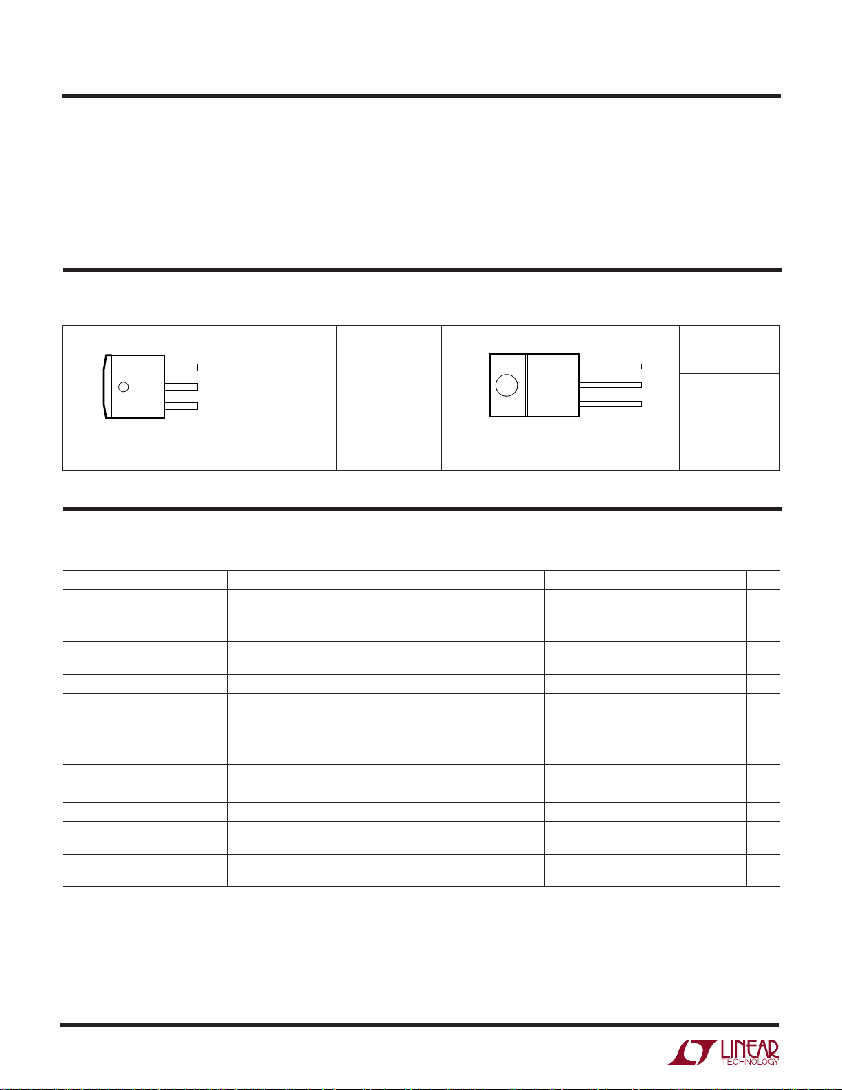
The LT1585-1.5/LT1585A-1.5 are available in the throughhole 3-pin TO-220 power package and 3-pin plastic DD.
, LTC and LT are registered trademarks of Linear Technology Corporation.
3.3V
LT1585A-1.5
V
C1, C2
+
100µF
10V
NOTE: LTC RECOMMENDS CENTRALLY
LOCATING THE LT1585A-1.5 TO MINIMIZE
DISTRIBUTION DROPS AND USING
V
TT
SEPARATE V
BUS END
V
IN
OUT
GND
GENERATORS AT EACH
REF
+
V
5A
TT
= 1.5V
C3 TO C6
100µF
10V
Intel Processor GTL+ Supply
C7 TO
C12
1µF
RX
TX
RX
R1
75Ω
V
REF
R2
150Ω
TX
C13
0.1µF
Q1
Q3
R5
100ΩR7100ΩR8100ΩR6100Ω
•
•
•
142 TOTAL SIGNAL LINES
R3
V
75Ω
REF
R4
150Ω
Q2
Q4
C14
0.1µF
RX
TX
RX
TX
1585-1.5 • TA01
1
Page 2
LT1585-1.5/LT1585A-1.5
WW
W
ABSOLUTE MAXIMUM RATINGS
U
(Note 1)
VIN............................................................................ 7V
Operating Junction Temperature Range
Control Section .................................. 0°C to 125°C
Power Transistor ................................ 0°C to 150°C
U
W
PACKAGE/ORDER INFORMATION
FRONT VIEW
TAB
IS
OUTPUT
Consult factory for Industrial and Military grade parts.
3
2
1
M PACKAGE
3-LEAD PLASTIC DD
θJA = 30°C/W*
*WITH PACKAGE
SOLDERED TO 0.5
V
IN
SQUARE INCH COPPER
AREA OVER BACKSIDE
V
OUT
GROUND PLANE OR
INTERNAL POWER PLANE.
GND
CAN VARY FROM
θ
JA
20°C/W TO >40°C/W
WITH OTHER MOUNTING
TECHNIQUES
ORDER PART
NUMBER
LT1585CM-1.5
LT1585ACM-1.5
Storage Temperature Range ................ –65°C to 150°C
Lead Temperature (Soldering, 10 sec)................. 300°C
UUU
PRECONDITIONI G
100% Thermal Limit Functional Test
U
ORDER PART
IN
OUT
LT1585CT-1.5
LT1585ACT-1.5
TAB IS
OUTPUT
FRONT VIEW
3
2
1
T PACKAGE
3-LEAD PLASTIC TO-220
θJA = 50°C/W
V
V
GND
NUMBER
ELECTRICAL CHARACTERISTICS
The ● denotes specifications which apply over the specified operating
temperature range, otherwise specifications are at TA = 25°C.
PARAMETER CONDITIONS MIN TYP MAX UNITS
Output Voltage (Note 4) VIN = 5V, TJ = 25°C, I
Line Regulation (Notes 2, 3) 3V ≤ VIN ≤ 7V, I
Load Regulation VIN = 5V, TJ = 25°C, 0mA ≤ I
(Notes 2, 3, 4) ● 0.05 0.5 %
Dropout Voltage (Note 4) ∆V
Current Limit LT1585-1.5, (V
Quiescent Current V
Ripple Rejection (Note 4) f = 120Hz, C
Thermal Regulation TA = 25°C, 30ms Pulse 0.004 0.02 %/W
Temperature Stability ● 0.5 %
Long-Term Stability TA = 125°C, 1000 Hrs. 0.03 1.0 %
RMS Output Noise TA = 25°C, 10Hz ≤ f ≤ 10kHz 0.003 %
(% of V
Thermal Resistance T Package: Control Circuitry/Power Transistor 0.7/3.0 °C/W
Junction to Case M Package: Control Circuitry/Power Transistor 0.7/3.0 °C/W
Note 1: Absolute Maximum Ratings are those values beyond which the life
of the device may be impaired.
Note 2: See thermal regulation specifications for changes in output voltage
due to heating effects. Load and line regulation are measured at a constant
junction temperature by low duty cycle pulse testing.
Note 3: Line and load regulation are guaranteed up to the maximum
power dissipation (25W for the LT1585-1.5 in T package and 27.5W for
OUT
)
≤ 7V, 0mA ≤ I
3V ≤ V
IN
= 1%, I
OUT
LT1585A-1.5, (V
= 5V ● 713 mA
IN
OUT
IN
OUT
= 0mA 1.485 (–1%) 1.5 1.515 (+1%) V
OUT
≤ I
OUT
FULL LOAD
= 0mA 0.005 0.2 %
OUT
≤ I
OUT
FULL LOAD
= I
FULL LOAD
– V
) = 5.5V ● 4.60 5.25 A
OUT
– V
IN
= 25µF Tant., VIN = 4.5V, I
) = 5.5V ● 5.00 6.00 A
OUT
= I
OUT
FULL LOAD
the LT1585A-1.5). Power dissipation is determined by input/output
differential and the output current. Guaranteed maximum output power
will not be available over the full input/output voltage range.
Note 4: I
FULL LOAD
as a function of input-to-output voltage. I
LT1585-1.5 and 5A for the LT1585A-1.5. The LT1585-1.5/LT1585A-1.5
have constant current limit with changes in input-to-output voltage.
● 1.470 (–2%) 1.5 1.530 (+2%) V
0.05 0.3 %
● 1.200 1.400 V
● 60 72 dB
is defined as the maximum value of output load current
FULL LOAD
is equal to 4.6A for the
2
Page 3
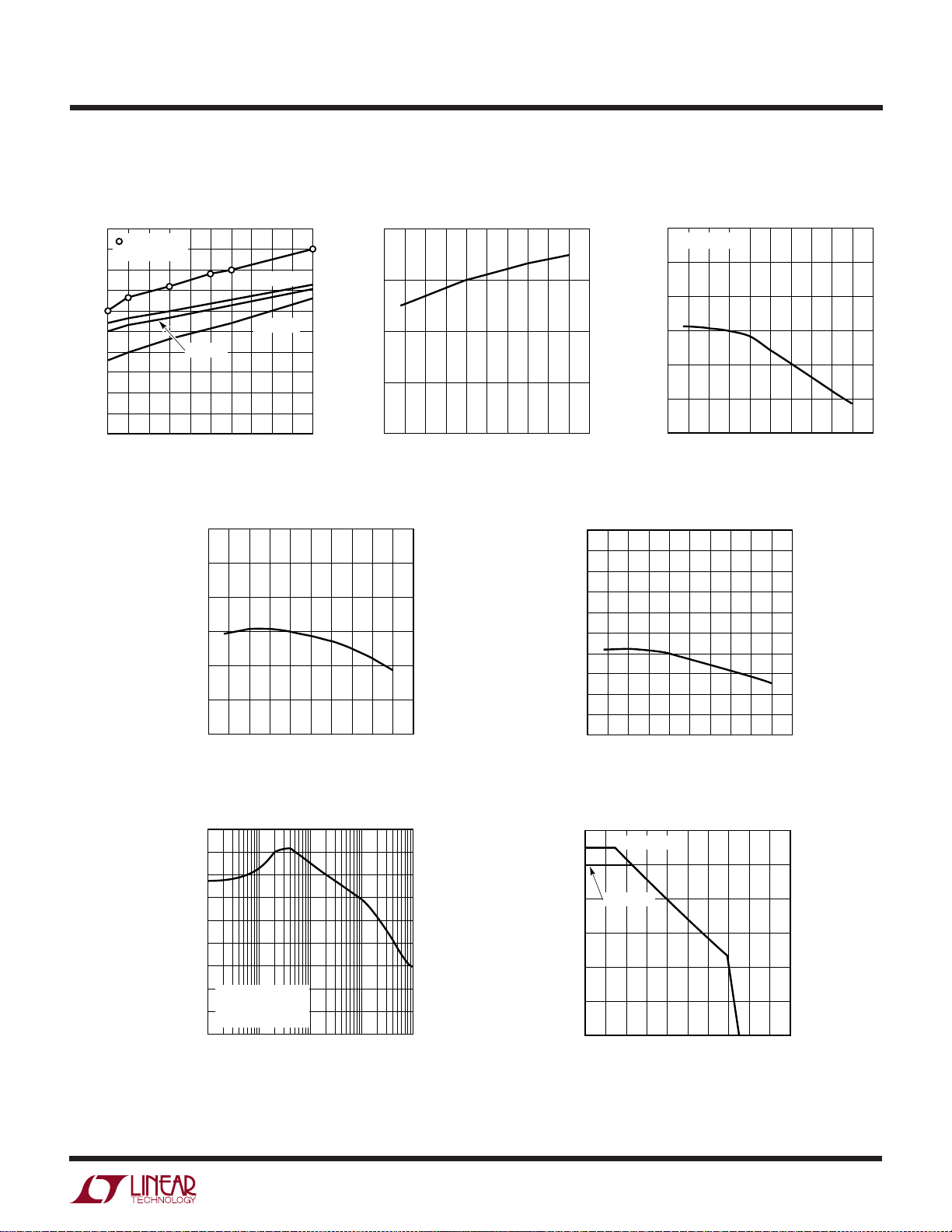
W
TEMPERATURE (°C)
–0.20
OUTPUT VOLTAGE DEVIATION (%)
–0.10
0
0.10
–0.15
–0.05
0.05
–25 25 75 125
1585-1.5 G03
175–50–75 0 50 100 150
∆I = I
FULL LOAD
U
TYPICAL PERFORMANCE CHARACTERISTICS
LT1585-1.5/LT1585A-1.5
LT1585A-1.5 Dropout Voltage vs
Output Current
1.5
GUARANTEED
1.4
TEST POINTS
1.3
1.2
1.1
1.0
0.9
0.8
DROPOUT VOLTAGE (V)
0.7
0.6
0.5
0
T = 25°C
1
2
OUTPUT CURRENT (A)
3
Output Voltage vs Temperature
1.53
1.52
1.51
1.50
1.49
OUTPUT VOLTAGE (V)
1.48
1.47
–25 25 75 125
T = –5°C
T = 125°C
4
5
1585-1.5 G01
TEMPERATURE (°C)
LT1585A-1.5 Short-Circuit Current
vs Temperature
6.0
5.5
5.0
4.5
SHORT-CIRCUIT CURRENT (A)
4.0
–50
–75
1585-1.5 G04
–25
175–50–75 0 50 100 150
50
75
0
25
TEMPERATURE (°C)
100
Load Regulation vs Temperature
125
175
150
1585-1.5 G02
Quiescent Current vs Temperature
13
12
11
10
9
8
7
6
QUIESCENT CURRENT (mA)
5
4
3
–25
0
–50 150
–75
25
50
TEMPERATURE (°C)
75
100
125
175
1585-1.5 G05
Ripple Rejection vs Frequency
90
80
70
60
50
40
30
RIPPLE REJECTION (dB)
20
(VIN – V
0.5V ≤ V
10
I
OUT
0
10 1k 10k 100k
OUT
= I
FULL LOAD
100
RIPPLE
) ≤ 3V
≤ 2V
FREQUENCY (Hz)
1585-1.5 G06
Maximum Power Dissipation*
30
25
20
15
POWER (W)
10
5
0
*AS LIMITED BY MAXIMUM JUNCTION TEMPERATURE
50
LT1585A-1.5
LT1585-1.5
90 110 120 130 140 150
80 100
60 70
CASE TEMPERATURE (˚C)
1585-1.5 G07
3
Page 4

LT1585-1.5/LT1585A-1.5
WW
SI PLIFIED SCHE ATIC
V
IN
THERMAL
LIMIT
GND
+
–
V
OUT
1585-1.5 SS
U
WUU
APPLICATIONS INFORMATION
General
The LT1585-1.5/LT1585A-1.5 3-terminal regulators are
easy to use and have all the protection features expected
in high performance linear regulators. The devices are
short-circuit protected, safe-area protected and provide
thermal shutdown to turn off the regulators if the junction
temperature exceeds about 150°C.
The ICs are pin compatible with the LT1083/LT1084/LT1085
family of linear regulators but offer lower dropout voltage
and faster transient response. The trade-off for this improved performance is a 7V maximum supply voltage.
Similar to the LT1083/LT1084/LT1085 family, the LT1585-
1.5/LT1585A-1.5 regulators require an output capacitor for
stability. However, the improved frequency compensation
permits the use of capacitors with much lower ESR while still
maintaining stability. This is critical in addressing the needs
of modern low voltage, high speed microprocessors.
Current generation microprocessors and their associated
circuitry cycle load current from almost zero to several
amps in tens of nanoseconds. Output voltage tolerances
are tighter and include transient response as part of the
specification. The LT1585-1.5/LT1585A-1.5 are specifically designed to meet the fast current load step require-
ments of these applications and save total cost by needing
less output capacitance in order to maintain regulation.
Stability
The circuit design in the LT1585-1.5/LT1585A-1.5 requires the use of an output capacitor as part of the
frequency compensation. For all operating conditions, the
addition of a 22µF solid tantalum or a 100µF aluminum
electrolytic on the output ensures stability. Normally, the
LT1585-1.5/LT1585A-1.5 can use smaller value capacitors. Many different types of capacitors are available and
have widely varying characteristics. These capacitors differ
in capacitor tolerance (sometimes ranging up to ±100%),
equivalent series resistance, equivalent series inductance
and capacitance temperature coefficient. The LT1585-1.5/
LT1585A-1.5 frequency compensation optimizes frequency
response with low ESR capacitors. In general, use capacitors with an ESR of less than 1Ω.
Normally, capacitor values on the order of several hundred
microfarads are used on the output of the regulators to
ensure good transient response with heavy load current
changes. Output capacitance can increase without limit
and larger values of output capacitance further improve the
4
Page 5
LT1585-1.5/LT1585A-1.5
U
WUU
APPLICATIONS INFORMATION
stability and transient response of the LT1585-1.5/
LT1585A-1.5.
Large load current changes are exactly the situation presented by modern microprocessors and their peripheral
circuitry. The load current step contains higher order
frequency components that the output decoupling network
must handle until the regulator throttles to the load current
level. Capacitors are not ideal elements and contain parasitic resistance and inductance. These parasitic elements
dominate the change in output voltage at the beginning of
a transient load step change. The ESR of the output
capacitors produces an instantaneous step in output voltage [∆V = ∆I(ESR)]. The ESL of the output capacitors
produces a droop proportional to the rate of change of
output current [V = L(∆I/∆t)]. The output capacitance
produces a change in output voltage proportional to the
time until the regulator can respond [∆V = ∆t(∆I/C)]. These
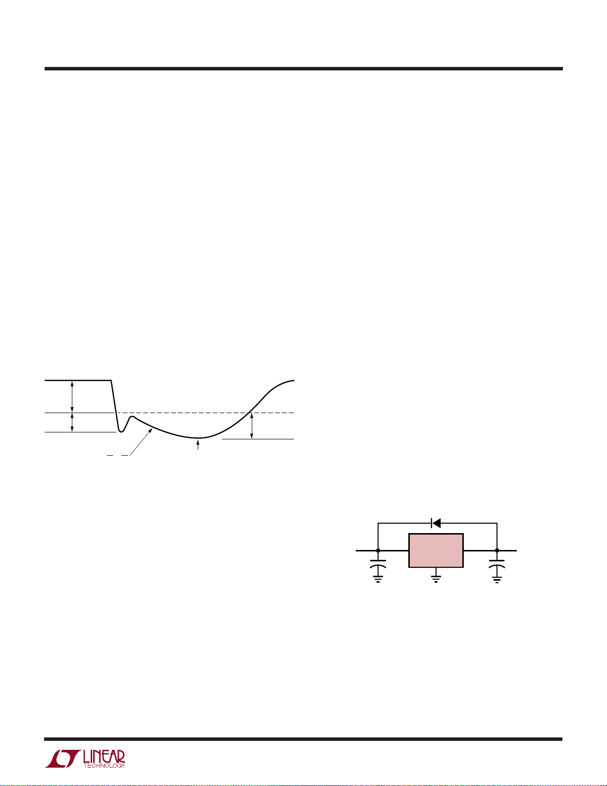
transient effects are illustrated in Figure 1.
ESR
EFFECTS
ESL
EFFECTS
V
SLOPE, =
∆I
t
C
POINT AT WHICH REGULATOR
TAKES CONTROL
Figure 1
The use of capacitors with low ESR, low ESL and good high
frequency characteristics is critical in meeting the output
voltage tolerances of these high speed microprocessor
applications. These requirements dictate a combination of
high quality surface mount tantalum capacitors and ceramic capacitors. The location of the decoupling network is
critical to transient response performance. Place the
decoupling network as close as possible to the microprocessor control circuitry because a trace run from the
decoupling capacitors to the actual circuitry is inductive. In
addition, use large power and ground plane areas to
minimize distribution drops.
A possible stability problem that occurs in monolithic linear
regulators is current limit oscillations. The LT1585-1.5/
LT1585A-1.5 essentially have a flat current limit over the
CAPACITANCE
EFFECTS
1585-1.5 F01
range of input supply voltage. The lower current limit rating
and 7V maximum supply voltage rating for this device
permit this characteristic. Current limit oscillations are
typically nonexistent unless the input and output decoupling capacitors for the regulators are mounted several
inches from the terminals.
Protection Diodes
In normal operation, the LT1585-1.5/LT1585A-1.5 do not
require any protection diodes. Older 3-terminal regulators
require protection diodes between the output pin and the
input pin to prevent die overstress.
A protection diode between the input and output pins is
usually not needed. An internal diode between the input
and output pins on the LT1585-1.5/LT1585A-1.5 can
handle microsecond surge currents of 50A to 100A. Even
with large value output capacitors it is difficult to obtain
those values of surge currents in normal operation. Only
with large values of output capacitance, such as 1000µF to
5000µF, and with the input pin instantaneously shorted to
ground can damage occur. A crowbar circuit at the input of
the LT1585-1.5/LT1585A-1.5 can generate those levels of
current and a diode from output to input is then recommended. This is shown in Figure 2. Usually, normal power
supply cycling or system “hot plugging and unplugging”
will not generate current large enough to do any damage.
D1
1N4002
(OPTIONAL)
LT1585-1.5
V
IN
+ +
C1
10µF
IN OUT
GND
Figure 2
C2
10µF
V
OUT
1585-1.5 F02
Ripple Rejection
The typical curve for ripple rejection reflects values for the
LT1585-1.5/LT1585A-1.5 as a function of frequency. In
applications that require improved ripple rejection, use the
adjustable LT1585/LT1585A. A bypass capacitor from the
adjust pin to ground reduces the output ripple by the ratio
of V
OUT
/1.25V.
5
Page 6

LT1585-1.5/LT1585A-1.5
U
WUU
APPLICATIONS INFORMATION
Load Regulation
It is not possible to provide true remote load sensing
because the LT1585-1.5/LT1585A-1.5 are 3-terminal devices. Load regulation is limited by the resistance of the
wire connecting the regulators to the load. Load regulation
per the data sheet specification is measured at the bottom
of the package.
For fixed voltage devices, negative side sensing is a true
Kelvin connection with the GND pin of the device returned
to the negative side of the load. This is illustrated in
Figure 3.
R
P
PARASITIC
V
IN
LT1585-1.5
IN OUT
GND
LINE RESISTANCE
1585-1.5 F03
R
L
Junction-to-case thermal resistance is specified from the
IC junction to the bottom of the case directly below the die.
This is the lowest resistance path for heat flow. Proper
mounting ensures the best thermal flow from this area of
the package to the heat sink. Linear Technology strongly
recommends thermal compound at the case-to-heat sink
interface. Use a thermally conductive spacer if the case of
the device must be electrically isolated and include its
contribution to the total thermal resistance. Please consult
“Mounting Considerations for Power Semiconductors”
1990 Linear Applications Handbook, Volume I
, Pages
RR3-1 to RR3-20. The output connects to the case of the
device in the LT1585-1.5/LT1585A-1.5.
For example, using an LT1585ACT-1.5 (TO-220, commercial) and assuming:
V
(Max Continuous) = 3.465V (3.3V + 5%), V
IN
I
= 5A
OUT
TA = 70°C, θ
HEAT SINK
= 3°C/W
OUT
= 1.5V
Figure 3. Connection for Best Load Regulation
Thermal Considerations
The LT1585-1.5/LT1585A-1.5 protect the device under
overload conditions with internal power and thermal limiting circuitry. However, for normal continuous load conditions, do not exceed maximum junction temperature ratings. It is important to consider all sources of thermal
resistance from junction-to-ambient. These sources include the junction-to-case resistance, the case-to-heat
sink interface resistance, and the heat sink resistance.
Thermal resistance specifications have been developed to
more accurately reflect device temperature and ensure safe
operating temperatures. The electrical characteristics section provides a separate thermal resistance and maximum
junction temperature for both the control circuitry and the
power transistor. Older regulators with a single junctionto-case thermal resistance specification, use an average of
the two values provided here and allow excessive junction
temperatures under certain conditions of ambient temperature and heat sink resistance. Calculate the maximum
junction temperature for both sections to ensure that both
thermal limits are met.
θ
CASE-TO-HEAT SINK
= 1°C/W (with Thermal Compound)
Power dissipation under these conditions is equal to:
PD = (V
IN
– V
OUT
)(I
) = (3.465 – 1.5)(5A) = 9.825W
OUT
Junction temperature will be equal to:
TJ = TA + PD(θ
HEAT SINK
+ θ
CASE-TO-HEAT SINK
+ θJC)
For the Control Section:
TJ = 70°C + 9.825W (3°C/W + 1°C/W + 0.7°C/W) = 116.2°C
116.2°C < 125°C = T
(Control Section Commercial
JMAX
Range)
For the Power Transistor:
TJ = 70°C + 9.825W (3°C/W + 1°C/W + 3°C/W) = 138.8°C
138.8°C < 150°C = T
(Power Transistor Commercial
JMAX
Range)
In both cases the junction temperature is below the maximum rating for the respective sections, ensuring reliable
operation.
6
Page 7

PACKAGE DESCRIPTION
LT1585-1.5/LT1585A-1.5
U
Dimensions in inches (millimeters) unless otherwise noted.
M Package
3-Lead Plastic DD Pak
(LTC DWG # 05-08-1460)
0.256
(6.502)
0.060
(1.524)
0.300
(7.620)
BOTTOM VIEW OF DD PAK
HATCHED AREA IS SOLDER PLATED
COPPER HEAT SINK
(1.524)
(1.905)
0.060
0.075
0.183
(4.648)
0.060
(1.524)
TYP
0.330 – 0.370
(8.382 – 9.398)
+0.012
0.143
–0.020
+0.305
3.632
()
–0.508
0.050
(1.270)
BSC
0.390 – 0.415
(9.906 – 10.541)
15
° TYP
0.090 – 0.110
(2.286 – 2.794)
T Package
3-Lead Plastic TO-220
(LTC DWG # 05-08-1420)
0.165 – 0.180
(4.191 – 4.572)
0.059
(1.499)
TYP
0.013 – 0.023
(0.330 – 0.584)
0.045 – 0.055
(1.143 – 1.397)
+0.008
0.004
–0.004
+0.203
0.102
()
–0.102
0.095 – 0.115
(2.413 – 2.921)
± 0.012
0.050
(1.270 ± 0.305)
M (DD3) 1098
0.390 – 0.415
(9.906 – 10.541)
0.460 – 0.500
(11.684 – 12.700)
0.980 – 1.070
(24.892 – 27.178)
0.520 – 0.570
(13.208 – 14.478)
0.147 – 0.155
(3.734 – 3.937)
DIA
0.230 – 0.270
(5.842 – 6.858)
0.570 – 0.620
(14.478 – 15.748)
0.330 – 0.370
(8.382 – 9.398)
0.218 – 0.252
(5.537 – 6.401)
0.100
(2.540)
BSC
0.028 – 0.038
(0.711 – 0.965)
Information furnished by Linear Technology Corporation is believed to be accurate and reliable.
However, no responsibility is assumed for its use. Linear Technology Corporation makes no representation that the interconnection of its circuits as described herein will not infringe on existing patent rights.
0.050
(1.270)
TYP
0.165 – 0.180
(4.191 – 4.572)
0.013 – 0.023
(0.330 – 0.584)
0.045 – 0.055
(1.143 – 1.397)
0.095 – 0.115
(2.413 – 2.921)
T3 (TO-220) 1098
7
Page 8

LT1585-1.5/LT1585A-1.5
RELATED PARTS
PART NUMBER DESCRIPTION COMMENTS
LTC®1392 Micropower Temperature, Power Supply and Differential Voltage Monitor Micropower Data Acquisition to Monitor System
LTC1530 High Power Step-Down Synchronous DC/DC Controller in SO-8 Synchronous Operation Up to 15A, Fixed or Adj Outputs
LT1528 Low Dropout 3A Linear Regulator 0.6V Dropout for 5V to 4V Regulation
LT1573 Low Dropout Regulator Driver Drives Low Cost PNP, Fast Transient Response
LT1575 UltrafastTM Transient Response Low Dropout Regulator Driver Drives N-Channel MOSFET Up to 10A, SO-8
LT1580 Very Low Dropout 7A Linear Regulator 0.54V Dropout at 7A, Fixed 2.5V
Ultrafast is a trademark of Linear Technology Corporation.
or Adjustable
OUT
8
Linear Technology Corporation
1630 McCarthy Blvd., Milpitas, CA 95035-7417
(408) 432-1900 ● FAX: (408) 434-0507
●
www.linear-tech.com
158515fa LT/TP 0100 2K REV A • PRINTED IN USA
LINEAR TECHNOLOGY CORPORATION 1996
 Loading...