

Page 1
FEATURES
■
Greatly Reduced Conducted and Radiated EMI
■
Low Switching Harmonic Content
■
Independent Control of Switch Voltage and
Current Slew Rates
■
2A Current Limited Power Switch
■
Regulates Positive and Negative Voltages
■
20kHz to 250kHz Oscillator Frequency
■
Easily Synchronized to External Clock
■
Wide Input Voltage Range: 2.7V to 23V
■
Low Shutdown Current: 12µA Typical
■
Easier Layout than with Conventional Switchers
U
APPLICATIO S
■
Precision Instrumentation Systems
■
Isolated Supplies for Industrial Automation
■
Medical Instruments
■
Wireless Communications
■
Single Board Data Acquisition Systems
LT1534/LT1534-1
Ultralow Noise
2A Switching Regulators
U
DESCRIPTIO
The LT®1534/LT1534-1 are a new class of switching regulator designed to reduce conducted and radiated electromagnetic interference (EMI). Ultralow noise and EMI are achieved
by providing user control of the output switch slew rates.
Voltage and current slew rates can be independently programmed to optimize switcher harmonic content versus
efficiency. The LT1534/LT1534-1 can reduce high frequency
harmonic power by as much as 40dB with only minor losses
in efficiency.
The LT1534/LT1534-1 utilize a current mode architecture
optimized for low noise boost topologies. The ICs include a
2A power switch along with all necessary oscillator, control
and protection circuitry. Unique error amp circuitry can
regulate both positive and negative voltages. The internal
oscillator may be synchronized to an external clock for more
accurate placement of switching harmonics. Protection features include cycle-by-cycle current limit protection, undervoltage lockout and thermal shutdown.
Low minimum supply voltage and low supply current during
shutdown make the LT1534/LT1534-1 well suited for portable applications. The LT1534/LT1534-1 are available in the
16-pin narrow SO package.
, LTC and LT are registered trademarks of Linear Technology Corporation.
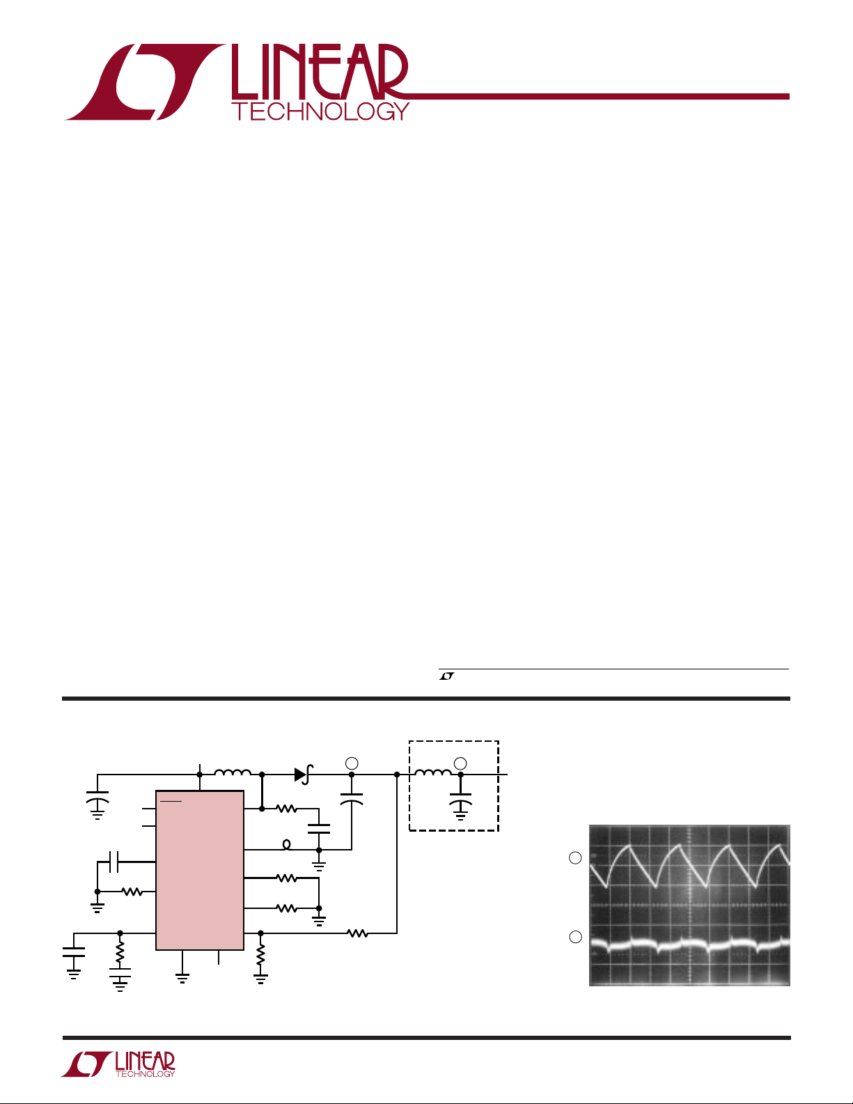
TYPICAL APPLICATION
L1
3.3V
50µH
+
220pF
C
33µF
6.3V
3300pF
IN
16.9k
6.8k
15nF
12
SHDN
4
SYNC
5
C
6
R
11
V
15
V
T
T
C
GND
IN
LT1534-1
9,16
PGND
NFB
R
R
101,8,
COL
VSL
CSL
2
3
14
13
7
FB
2.49k
Figure 1. Low Noise 3.3V to 5V Boost Converter
U
1N5817
10Ω
L2
24k
24k
A
C1
+
47µF
6.3V
×2
1nF
7.5k
CIN: MATSUSHITA ECGCOJB330
C1, C2: MATSUSHITA ECGCOJB47O
L1, L3: COILTRONICS CTX50-4
L2: COILCRAFT B08T (28nH) OR PC TRACE
1534 TA01
L3
50µH
OPTIONAL
B
+
C2
47µF
5V
650mA
50mV/DIV
2mV/DIV
5V Output Noise (BW = 100MHz)
A
B
10µs/DIV
1534 TA02
1
Page 2

LT1534/LT1534-1
WW
W
ABSOLUTE MAXIMUM RATINGS
U
(Note 1)
Input Voltage (VIN) .................................................. 30V
Switch Voltage (COL) .............................................. 35V
SHDN Pin Voltage.................................................... 30V
Feedback Pin Current (FB) .................................... 10mA
Negative Feedback Pin Current (NFB) .................. ±10mA
U
W
U
PACKAGE/ORDER INFORMATION
ORDER PART
NUMBER
LT1534CS
LT1534IS
1
NC
2
COL
3
*NC
4
SYNC
5
C
T
6
R
T
7
FB
8
NFB
16-LEAD PLASTIC SO
*DO NOT CONNECT
T
JMAX
TOP VIEW
16
15
14
13
12
11
10
9
S PACKAGE
= 125°C, θJA = 100°C/W
PGND
COL
V
IN
R
VSL
R
CSL
SHDN
V
C
GND
Operating Junction Temperature Range
LT1534C................................................ 0°C to 125°C
LT1534I ............................................ –40°C to 125°C
Maximum Junction Temperature .......................... 125°C
Storage Temperature Range ................. –65°C to 150°C
Lead Temperature (Soldering, 10 sec.)................. 300°C
TOP VIEW
1
GND
2
COL
3
PGND
4
SYNC
5
C
T
6
R
T
7
FB
8
GND
S PACKAGE
**FOUR CORNER PINS ARE FUSED TO INTERNAL
CONNECT THESE FOUR PINS TO EXPANDED
16-LEAD PLASTIC SO
DIE ATTACH PADDLE FOR HEAT SINKING.
PC LANDS FOR PROPER HEAT SINKING.
T
= 125°C, θJA = 50°C/W
JMAX
16
GND
15
V
IN
14
R
VSL
13
R
CSL
12
SHDN
11
V
C
10
NFB
9
GND
ORDER PART
NUMBER
LT1534CS-1
LT1534IS-1
Consult factory for Military grade parts.
ELECTRICAL CHARACTERISTICS
temperature range, otherwise specifications are at TA = 25°C, VIN = 5V, VC = 0.9V, VFB = V
The ● denotes the specifications which apply over the full operating
. COL, SHDN, NFB, all other pins open
REF
unless otherwise noted.
SYMBOL PARAMETER CONDITIONS MIN TYP MAX UNITS
Supply and Protection
V
IN
V
IN(MIN)
I
VIN
I
VIN(OFF)
V
SHDN
I
SHDN
Error Amplifiers
V
REF
I
FB
FB
REG
Recommended Operating Range ● 2.7 23 V
Minimum Input Voltage ● 2.55 2.7 V
Operating Supply Current 2.7V ≤ VIN ≤ 23V, R
Shutdown Supply Current 2.7V ≤ VIN ≤ 23V, V
2.7V ≤ V
≤ 23V, V
IN
, R
VSL
SHDN
SHDN
, RT = 17k ● 12 30 mA
CSL
= 0V ● 12 50 µA
= 0V 12 30 µA
Shutdown Threshold 2.7V ≤ VIN ≤ 23V ● 0.4 0.8 1.2 V
Shutdown Input Current –2 µA
Reference Voltage Measured at Feedback Pin 1.235 1.250 1.265 V
● 1.215 1.250 1.275 V
Feedback Input Current VFB = V
REF
● 250 900 nA
Reference Voltage Line Regulation 2.7V ≤ VIN ≤ 23V ● 0.003 0.03 %/V
2
Page 3
LT1534/LT1534-1
ELECTRICAL CHARACTERISTICS
temperature range, otherwise specifications are at TA = 25°C, VIN = 5V, VC = 0.9V, VFB = V
The ● denotes the specifications which apply over the full operating
. COL, SHDN, NFB, all other pins open
REF
unless otherwise noted.
SYMBOL PARAMETER CONDITIONS MIN TYP MAX UNITS
Error Amplifiers
V
NFR
I
NFR
NFB
REG
g
m
I
ESK
I
ESRC
V
CLH
V
CLL
A
V
Oscillator and Sync
f
MAX
f
SYNC
R
SYNC
V
FBfs
Output Switches
DC
MAX
t
IBL
BV
COL
R
ON
I
LIM
∆IIN/∆I
Slew Control
V
SLEWR
V
SLEWF
I
SLEWR
I
SLEWF
Note 1: Absolute Maximum Ratings are those values beyond which the life
of a device may be impaired.
Negative Feedback Reference Voltage Measured at Negative Feedback Pin with ● –2.550 –2.500 –2.420 V
Feedback Pin Open
Negative Feedback Input Current V
NFB
= V
NFR
● –37 –25 µA
Negative Feedback Reference Voltage 2.7V ≤ VIN ≤ 23V ● 0.002 0.05 %/V
Line Regulation
Error Amplifier Transconductance ∆IC = ±25µA 1100 1500 1900 µmho
● 700 2300 µmho
Error Amplifier Sink Current VFB = V
Error Amplifier Source Current VFB = V
+ 150mV, VC = 0.9V, V
REF
– 150mV, VC = 0.9V, V
REF
= 1V ● 120 200 350 µA
SHDN
= 1V ● 120 200 350 µA
SHDN
Error Amplifier Clamp Voltage High Clamp, VFB = 1V 1.33 V
Error Amplifier Clamp Voltage Low Clamp, VFB = 1.5V 0.1 V
Error Amplifier Voltage Gain 180 250 V/V
Maximum Switch Frequency 250 kHz
Synchronization Frequency Range f
= 250kHz ● 375 kHz
OSC
SYNC Pin Input Resistance 40 kΩ
FB Pin Threshold for Frequency Shift 5% Reduction from Nominal 0.4 V
Maximum Switch Duty Cycle R
VSL
= R
CSL
= 4.9k, f
= 25kHz ● 88 91 %
OSC
Switch Current Limit Blanking Time 200 ns
Output Switch Breakdown Voltage 2.7V ≤ VIN ≤ 23V ● 35 V
Output Switch-On Resistance I
= 1.5A, Both COL Pins Tied Together ● 0.25 0.43 Ω
COL
Switch Current Limit Duty Cycle = 30% 2 A
Duty Cycle = 80% 1.6 A
Supply Current Increase During 16 mA/A
SW
Switch-On Time
Output Voltage Slew Rising Edge R
Output Voltage Slew Falling Edge R
Output Current Slew Rising Edge R
Output Current Slew Falling Edge R
VSL
VSL
VSL
VSL
, R
= 17k 11 V/µs
CSL
, R
= 17k 14.5 V/µs
CSL
, R
= 17k 1.3 A/µs
CSL
, R
= 17k 1.3 A/µs
CSL
3
Page 4
LT1534/LT1534-1
UW
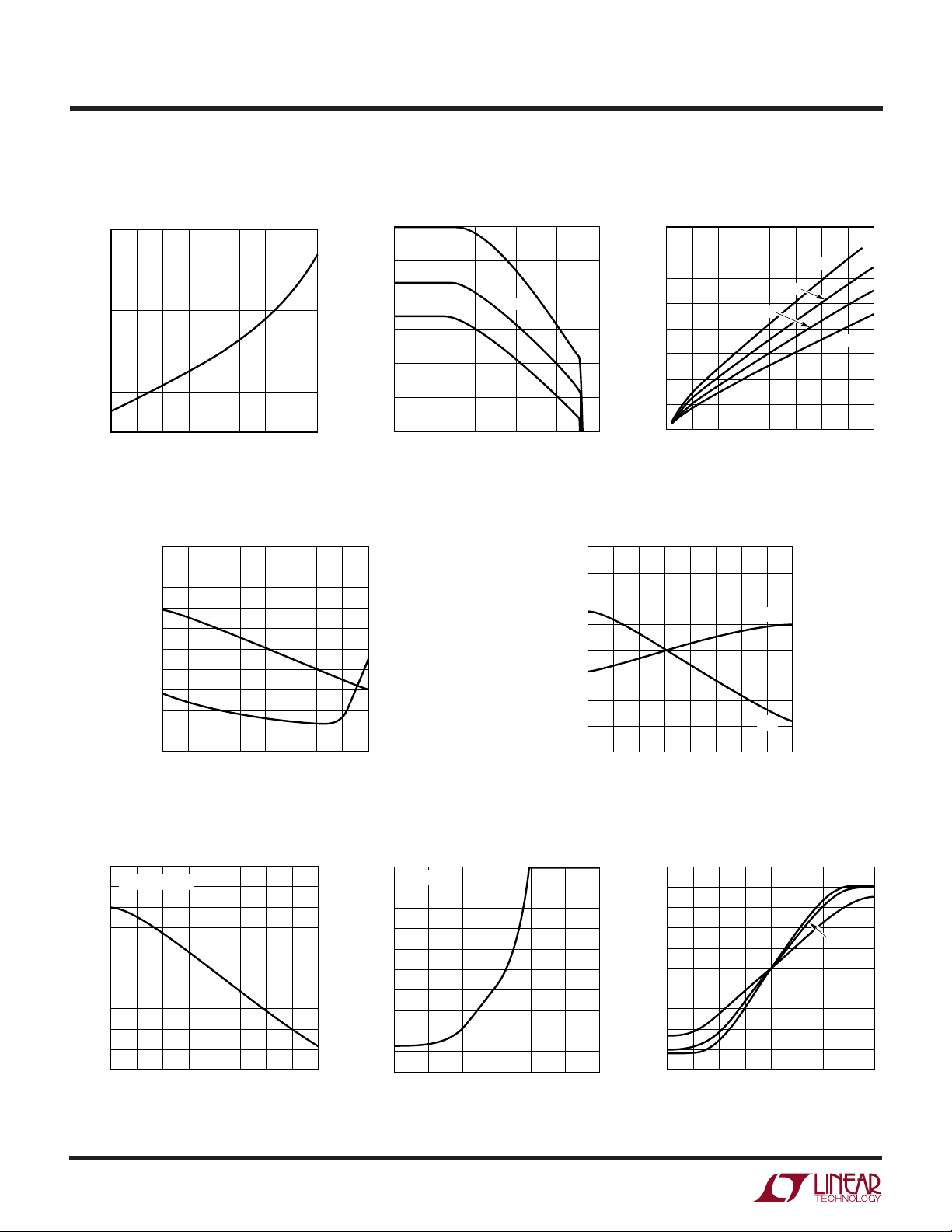
TYPICAL PERFORMANCE CHARACTERISTICS
Minimum Input Voltage (VIN)
vs Temperature
2.70
2.65
2.60
2.55
INPUT VOLTAGE (V)
2.50
2.45
–50
–25 25
0
JUNCTION TEMPERATURE (°C)
50
Feedback Voltage and
Input Current vs Temperature
1.30
1.29
1.28
1.27
1.26
1.25
1.24
1.23
FEEDBACK VOLTAGE (V)
1.22
1.21
1.20
–50
0
–25 25
125
100
75
1534 G01
V
FB
I
FB
50
TEMPERATURE (°C)
75
150
100
125
1533 G04
Change in Maximum Switch
–100
–200
(mA)
–300
LIM
∆I
–400
–500
–600
150
Current (I
0
0
2.0
1.8
FEEDBACK INPUT CURRENT (µA)
1.6
1.4
1.2
1.0
0.8
0.6
0.4
0.2
0
) vs Duty Cycle
LIM
125°C
20 40 60
DUTY CYCLE (%)
85°C
25°C
80
100
1533 G02
Negative Feedback Voltage and
Input Current vs Temperature
–2.30
–2.35
–2.40
–2.45
–2.50
–2.55
–2.60
NEGATIVE FB VOLTAGE (V)
–2.65
–2.70
–25 25 75
–50
Output Switch Saturation Voltage
vs Switch Current
0.8
0.7
0.6
0.5
0.4
0.3
SWITCH VOLTAGE (V)
0.2
0.1
0
0
0
TEMPERATURE (°C)
0.5
SWITCH CURRENT (A)
50
25°C
100
V
I
NFB
125
1.0
NFB
1533 G05
85°C
150
150°C
35
30
25
20
15
NFB IINPUT CURRENT (µA)
1.5
–40°C
2.0
1534 G03
Error Amplifier Transconductance
vs Temperature
2000
gm = ∆IVC/∆V
1900
1800
1700
1600
1500
1400
1300
1200
TRANSCONDUCTANCE (mho)
1100
1000
–50 25 75 150
–25 0
FB
50
TEMPERATURE (°C)
4
100 125
1534 G08
Switching Frequency vs
Feedback Pin Voltage
100
TA = 25°C
90
80
70
60
50
40
30
20
SWITCHING FREQUENCY (% TYPICAL)
10
0
0
0.1
FEEDBACK PIN VOLTAGE (V)
0.2
0.3 0.4
0.5
1533 G06
0.6
Error Amplifier Output Current (VC)
500
400
300
200
100
0
–100
–200
–300
ERROR AMPLIFIER OUTPUT (µA)
–400
–500
–400 –300 –200 –100
FEEDBACK PIN VOLTAGE FROM NOMINAL (mV)
–40°C
0 100 300
200
125°C
25°C
400
1534 G07
Page 5
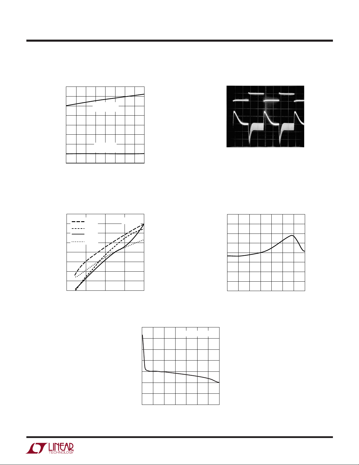
UW
TYPICAL PERFORMANCE CHARACTERISTICS
VC Pin Threshold and Clamp
Voltage vs Temperature
1.6
1.4
1.2
1.0
0.8
0.6
PIN VOLTAGE (V)
C
V
0.4
0.2
0
–50 25 75
–25 0
VC PIN CLAMP
THRESHOLD
TEMPERATURE (°C)
VOLTAGE
VC PIN
50
100 125
1534 G09
0.5A/DIV
100mV/DIV
LT1534/LT1534-1
Load Transient Response
I
LOAD
V
OUT
VIN = 3.3V 500µs/DIV 1534 G10
V
= 5V (NODE A)
OUT
= 0.1A TO 0.5A
I
LOAD
FIGURE 1 CIRCUIT
Typical Output Switch Voltage
and Current Slew Rates vs Slew
Setting Resistance (R
40
I
35
30
25
20
15
VOLTAGE SLEW (V/µs)
10
5
0
0 1/20k 1/10k 1/6.7k 1/5k
I
V
V
RISE
FALL
RISE
FALL
1/R (mmho)
VSL
= R
CSL
TA = 25°C
(%)
OUT
∆V
–0.5
)
4
CURRENT SLEW (A/µs)
3
2
1
0
1534 G11
Load Regulation
2.0
1.5
1.0
0.5
0
FIGURE 1 CIRCUIT
Percent Change in Oscillator
Frequency vs Temperature (NPO
Cap and Metal Film R)
2.0
1.5
1.0
0.5
0
–0.5
–1.0
CHANGE IN FREQUENCY (%)
–1.5
–2.0
–50
–25 25
0
TEMPERATURE (°C)
50
125
100
75
1534 G12
–1.0
–1.5
0
100 300
200
LOAD CURRENT (mA)
400
500
600
700
1534-1 G13
5
Page 6

LT1534/LT1534-1
UUU
PIN FUNCTIONS
(LT1534/LT1534-1)
COL (Pins 2, 15/Pin 2): These two pins should be con-
nected together externally to create the collector of the
power switch. The emitter returns to PGND through a
sense resistor. Large currents flow into these pins so it is
desirable to keep external trace lengths short to minimize
radiation.
SYNC (Pin 4): The SYNC pin can be used to synchronize
the oscillator to an external clock (see Oscillator Sync in
Applications Information section for more details). The
SYNC pin may either be floated or tied to ground if not
used.
CT (Pin 5): The oscillator capacitor pin is used in
conjunction with RT to set the oscillator frequency.
For RT = 16.9k,
C
= 129/f
T(NF)
RT (Pin 6): The oscillator resistor pin is used to set the
charge and discharge currents of the oscillator capacitor.
The nominal value is 16.9k. It is possible to adjust this
resistance ±25% to get a more accurate oscillator frequency.
FB (Pin 7): The feedback pin is used for positive voltage
sensing and oscillator frequency shifting during start-up
and short-circuit conditions. It is the inverting input to the
error amplifier. The noninverting input of this amplifier
connects internally to a 1.25V reference. This pin should
be left open if not used.
NFB (Pin 8/Pin 10): The negative voltage feedback pin is
used for sensing a negative output voltage. The pin is
connected to the inverting input of the negative feedback
amplifier through a 100k source resistor. The negative
feedback amplifier provides a gain of – 0.5 to the feedback
amplifier; therefore, the nominal regulation point is –2.5V
on NFB. This pin should be left open if not used.
GND (Pin 9/Pins 1, 8, 9, 16): Signal Ground. The internal
error amplifier, negative feedback amplifier, oscillator,
slew control circuitry and the bandgap reference are
OSC(kHz)
referred to this ground. Keep the connection to the feedback divider and VC compensation network free of large
ground currents.
VC (Pin 10/Pin 11): The compensation pin is used for
frequency compensation and current limiting. It is the
output of the error amplifier and the input of the current
comparator. Loop frequency compensation can be performed with an RC network connected from the VC pin to
ground.
SHDN (Pin 11/Pin 12): The shutdown pin is used for
disabling the switcher. Grounding this pin will disable all
internal circuitry. Normally this output can be tied high (to
VIN) or may be left floating.
R
(Pin 12/Pin 13): A resistor to ground sets the current
CSL
slew rate for the power switch. The minimum resistor
value is 3.9k and the maximum value is 68k. Current slew
will be approximately:
I
SLEW(A/µs)
R
(Pin 13/Pin 14): A resistor to ground sets the voltage
VSL
slew rate for the power switch collector. The minimum
resistor value is 3.9k and the maximum value is 68k.
Voltage slew will be approximately:
V
SLEW(V/µs)
VIN (Pin 14/Pin 15): Input Supply Pin. Bypass this pin with
a ≥ 4.7µF low ESR capacitor. When VIN is below 2.55V the
part will go into undervoltage lockout where it will stop
output switching and pull the VC pin low.
PGND (Pin 16/Pin 3): Power Switch Ground. This ground
comes from the emitters of the power switches. In normal
operation this pin should have approximately 25nH inductance to ground. This can be done by trace inductance
(approximately 1") or with wire or a specific inductive
component (e.g., small ferrite bead). This inductance
ensures stability in the current slew control loop during
turn-off. Too much inductance (>50nH) may produce
oscillation on the output voltage slew edges.
= 33/R
= 220/R
CSL(kΩ)
VSL(kΩ)
6
Page 7

BLOCK DIAGRA
V
C
+
NEGATIVE
FEEDBACK
AMP
–
NFB
SYNC
FB
R
T
C
T
100k 50k
W
1.25V
LT1534/LT1534-1
SHDN V
LDO REGULATOR
–
g
m
ERROR
AMP
+
+
OSCILLATOR
INTERNAL V
–
COMP
+
GND
IN
CC
PGND COL COL
+
–
SQ
FF
R
OUTPUT
DRIVER
SLEW CONTROL
1534 BD
R
VSL
R
CSL
U
OPERATIO
In noise sensitive applications, switching regulators tend
to be ruled out as a power supply option due to their
propensity for generating unwanted noise. When switching supplies are required due to efficiency or input/output
voltage constraints, great pains must be taken to work
around the noise generated by a typical supply. These
steps may include precise synchronization of the power
supply oscillator to an external clock, synchronizing the
rest of the circuit to the power supply oscillator, or halting
power supply switching during noise sensitive operations.
The LT1534 greatly simplifies the task of eliminating
supply noise by enabling the design of an inherently low
noise switching regulator power supply.
The LT1534 is a fixed frequency, current mode switching
regulator with unique circuitry to control the voltage and
current slew rates of the output switch. Slew control
capability provides much greater control over power supply components that can create conducted and radiated
electromagnetic interference. The current mode control
provides excellent AC and DC line regulation and simplifies
loop compensation.
Current Mode Control
A switching cycle begins with an oscillator discharge pulse
which resets the RS flip-flop, turning on the output driver
(refer to Block Diagram). The switch current is sensed
across an internal resistor and the resulting voltage is
amplified and compared to the output of the error amplifier
(VC pin). The driver is turned off once the output of the
current sense amplifier exceeds the voltage on the VC pin.
Internal slope compensation is provided to ensure stability under high duty cycle conditions.
Output regulation is obtained using the error amp to set
the switch current trip point. The error amp is a transconductance amplifier that integrates the difference between
the feedback output voltage and an internal 1.25V reference. The output of the error amp adjusts the switch
current trip point to provide the required load current at
the desired regulated output voltage. This method of
controlling current rather than voltage provides faster
input transient response, cycle by cycle current limiting
for better output switch protection and greater ease in
compensating the feedback loop.
The VC pin serves three different purposes. It is used for
loop compensation, current limit adjustment and soft
starting. During normal operation the VC voltage will be
between 0.2V and 1.33V. An external clamp may be used
for lowering the current limit. A capacitor coupled to an
external clamp can be used for soft starting.
7
Page 8

LT1534/LT1534-1
U
OPERATIO
The negative feedback amplifier allows for direct regulation of negative output voltages. The voltage on the NFB
pin gets amplified by a gain of – 0.5 and driven onto the FB
input, i.e., the NFB pin regulates to –2.5V while the
amplifier output internally drives the FB pin to 1.25V as in
normal operation. The negative feedback amplifier input
impedance is 100k (typ) referred to ground.
Slew Control
Control of output voltage and current slew rates is done via
two feedback loops. One loop controls the output switch
collector voltage dV/dt and the other loop controls the
emitter current dI/dt. Output slew control is achieved by
comparing the currents generated by these two slewing
events to currents created by external resistors R
R
. The two control loops are combined internally to
CSL
provide a smooth transition from current slew control to
voltage slew control.
U
WUU
VSL
and
APPLICATIONS INFORMATION
Internal Regulator
Most of the control circuitry operates from an internal 2.4V
low dropout regulator that is powered from VIN. The
internal low dropout design allows VIN to vary from 2.7V
to 23V with virtually no change in device performance.
When the part is put into shutdown, the internal regulator
is turned off, leaving only a small (12µA typ) current drain
from VIN.
Protection Features
There are three modes of protection in the LT1534. The
first is overcurrent limit. This is achieved via the clamping
action of the VC pin. The second is thermal shutdown that
disables both output drivers and pulls the VC pin low in the
event of excessive chip temperature. The third is undervoltage lockout that also disables both outputs
and pulls the VC pin low whenever VIN drops below 2.5V.
Reducing EMI from switching power supplies has traditionally invoked fear in designers. Many switchers are
designed solely on efficiency and as such produce waveforms filled with high frequency harmonics that then
propagate through the rest of the power supply.
The LT1534 provides control over two of the more important variables for controlling EMI with switching inductive
loads: switch voltage slew rate and switch current slew
rate. The use of this part will reduce noise and EMI over
conventional switch mode controllers. Because these
variables are under control, a supply built with this part will
exhibit far less tendency to create EMI and less chance of
wandering into problems during production.
It is beyond the scope of this data sheet to get into EMI
fundamentals. AN70 contains much information concerning noise in switching regulators and should be consulted.
Oscillator Frequency
The oscillator determines the switching frequency and
therefore the fundamental positioning of all harmonics.
The use of good quality external components is important
to ensure oscillator frequency stability. The oscillator is a
sawtooth design. A current defined by external resistor R
is used to charge and discharge the capacitor CT. The
discharge rate is approximately ten times the charge rate.
By allowing the user to have control over both components, trimming of oscillator frequency can be more easily
achieved.
The external capacitance CT is chosen by:
C
= 2180/[f
T(nF)
where f
For RT equal to 16.9k, this simplifies to:
C
T(nF)
(e.g., CT = 1.29nF for f
A good quality temperature stable capacitor should be
chosen.
Nominally RT should be 16.9k. Since it sets up current, its
temperature coefficient should be selected to compliment
the capacitor. Ideally, both should have low temperature
coefficients.
is the desired oscillator frequency in kHz.
OSC
= 129/f
OSC(kHz)
OSC(kHz)
• R
T(kΩ)
= 100kHz)
OSC
]
T
8
Page 9

LT1534/LT1534-1
U
WUU
APPLICATIONS INFORMATION
If the FB pin is below 0.4V the oscillator discharge time will
increase, causing the oscillation frequency to decrease by
approximately 6:1. This feature helps minimize power
dissipation during start-up and short-circuit conditions.
Oscillator frequency is important for noise reduction in
two ways: 1) the lower the oscillator frequency the lower
the harmonics of waveforms are, making it easier to filter
them, 2) the oscillator will control the placement of output
frequency harmonics which can aid in specific problems
where you might be trying to avoid a certain frequency
bandwidth that is used for detection elsewhere.
Oscillator Sync
If a more precise frequency is desired (e.g., to accurately
place harmonics) the oscillator can be synchronized to an
external clock. Set the RC timing components for an
oscillator frequency 10% lower than the desired sync
frequency.
Drive the SYNC pin with a square wave (with greater than
1.4V amplitude). The rising edge of the sync square wave
will initiate clock discharge. The sync pulse should have a
minimum of 0.5µs pulse width.
Be careful in synchronizing to frequencies much different
from the part since the internal oscillator charge slope
determines slope compensation. It would be possible to
get into subharmonic oscillation if the sync doesn’t allow
for the charge cycle of the capacitor to initiate slope
compensation. In general, this will not be a problem until
the sync frequency is greater than 1.5 times the oscillator
free-run frequency.
Slew Rate Setting
Setting the voltage and current slew rates is easy. External
resistors to ground on the R
the slew rates. Determining what slew rate to use is more
difficult. There are several ways to approach the problem.
First start by putting a 50k resistor pot with a 3.9k series
resistance on each pin. In general, the next step will be to
monitor the noise that you are concerned with. Be careful
in measurement technique (consult AN70). Keep probe
ground leads very short.
VSL
and R
pins determine
CSL
Usually it will be desirable to keep the voltage and current
slew resistors approximately the same. There are circumstances where a better optimization can be found by
adjusting each separately, but as these values are separated further, a loss of independence of control will occur.
Starting from the lowest resistor setting adjust the pots
until the noise level meets your guidelines. Note that
slower slewing waveforms will dissipate more power so
that efficiency will drop. You can also monitor this as you
make your slew adjustment.
It is possible to use a single slew setting resistor. In this
case the R
VSL
and R
pins are tied together. A resistor
CSL
with a value of 2k to 34k (one half the individual resistors)
can then be tied from these pins to ground.
Emitter Inductance
A small inductance in the power ground minimizes a
potential dip in the output current falling edge that can
occur under fast slewing, 25nH is usually sufficient. Greater
than 50nH may produce unwanted oscillations in the
voltage output. The inductance can be created by wire or
board trace with the equivalent of one inch of straight
length. A spiral board trace will require less length.
Positive Output Voltage Setting
Sensing of a positive output voltage is usually done using
a resistor divider from the output to the FB pin. The
positive input to the error amp is connected internally to a
1.25V bandgap reference. The FB pin will regulate to this
voltage.
R1
FB PIN
R2
Figure 2
V
OUT
1534 F01
Referring to Figure 2, R1 is determined by:
RR
12
V
OUT
125
.
1=−
The FB bias current represents a small error and can
usually be ignored for values of R1||R2 up to 10k.
9
Page 10

LT1534/LT1534-1
U
WUU
APPLICATIONS INFORMATION
One word of caution. Sometimes a feedback zero is added
to the control loop by placing a capacitor across R1 above.
If the feedback zero capacitively pulls the FB pin above the
internal regulator voltage (2.4V typ), output regulation
may be disrupted. A series resistance with the feedback
pin can eliminate this potential problem.
Negative Output Voltage Setting
Negative output voltage can be sensed using the NFB pin.
In this case regulation will occur when the NFB pin is at
–2.5V. The input bias current for the NFB pin is –25µA
(I
) and must be accounted for when selecting divider
NFB
resistor values.
R1
NFB PIN
I
NFB
R2
Figure 3
Referring to Figure 3, R1 is chosen such that:
–V
1534 F02
OUT
Thermal Considerations
Computing power dissipation for this IC requires careful
attention to detail. Reduced output slewing causes the part
to dissipate more power than would occur with fast edges.
However, much improvement in noise can be produced
with modest decrease in supply efficiency.
Power dissipation is a function of topology, input voltage,
switch current and slew rates. It is impractical to come up
with an all-encompassing formula. It is therefore recommended that package temperature be measured in each
application. The part has an internal thermal shutdown to
prevent device destruction, but this should not replace
careful thermal design.
1. Dissipation due to input current:
PVmA
=+
VIN IN
11
60
I
where I is the average switch current.
2. Dissipation due to the driver saturation:
.
−
=
RR
12
V
OUT
•
.•
+µ
25 2 25
25
RA
A suggested value for R2 is 2.5k. The NFB pin is normally
left open if the FB pin is being used.
Dual Polarity Output Voltage Sensing
Certain applications may benefit from sensing both positive and negative output voltages. When doing this each
output voltage resistor divider is individually set as previously described. When both FB and NFB pins are used, the
LT1534 will act to prevent either output from going
beyond its set output voltage. The highest output (lightest
load) will dominate control of the regulator. This technique
would prevent either output from going unregulated high
at no load. However, this technique will also compromise
output load regulation.
Shutdown
If the shutdown pin is pulled low, the regulator will turn off.
The supply current will be reduced to less than 20µA.
P
= (V
VSAT
where V
approximately 0.1 + (0.2)(I), DC
)(I)(DC
SAT
is the output saturation voltage which is
SAT
MAX
)
is the maximum
MAX
duty cycle.
3. Dissipation due to output slew using approximations
for slew rates:
Rf
()
()
VSL OSC
P
=
SLEW
Note if V
VI
IN
()
33 10
()
and ∆I are small with respect to VIN and I,
SAT
2
+
2
I
∆
4
R
()
CSL
9
IV
IN
()
+
220 10
()
2
V
−
SAT
4
9
2
then:
R
()
VSL
fVI
()()()
OSC IN
P
SLEW
IR
()( )
CSL
=
33 10 220 10
()
+
99
V
()
IN
()
10
Page 11

LT1534/LT1534-1
VC PIN
1534 F03
R
VC
2k
C
VC
0.01µF
C
VC2
4.7nF
U
WUU
APPLICATIONS INFORMATION
where ∆I is the ripple current in the switch, R
R
are the slew resistors and f
VSL
is the oscillator
OSC
frequency.
Power dissipation PD is the sum of these three terms. Die
junction temperature is then computed as:
TJ = T
where T
+ (PD)(θJA)
AMB
is ambient temperature and θJA is the package
AMB
thermal resistance. For the 16-pin SO with fused leads the
θJA is 50°C/W.
For example, with f
= 40kHz, 0.4A average current and
OSC
0.1A of ripple, the maximum duty cycle is 88%. Assume
slew resistors are both 17k and V
is 0.26V, then:
SAT
PD = 0.176W + 0.094W + 0.158W = 0.429W
In an S16 fused lead package the die junction temperature
would be 21°C above ambient.
Frequency Compensation
Loop frequency compensation is accomplished by way of
a series RC network on the output of the error amplifier (V
pin). Referring to Figure 4, the main pole is formed by
capacitor CVC and the output impedance of the error
amplifier (approximately 400kΩ). The series resistor R
creates a “zero” which improves loop stability and transient response. A second capacitor C
, typically one-
VC2
tenth the size of the main compensation capacitor, is
sometimes used to reduce the switching frequency ripple
on the VC pin. VC pin ripple is caused by output voltage
ripple attenuated by the output divider and multiplied by
the error amplifier. Without the second capacitor, VC pin
ripple is:
VgR
125.
V
CPIN RIPPLE
where V
()( )()()
RIPPLE
=
= Output ripple (V
RIPPLE m VC
V
OUT
)
P-P
gm = Error amplifier transconductance
RVC = Series resistor on VC pin
V
= DC output voltage
OUT
To prevent irregular switching, VC pin ripple should be
kept below 50mV
maximum output load current and will also be increased if
. Worst-case VC pin ripple occurs at
P-P
CSL
and
VC
poor quality (high ESR) output capacitors are used. The
addition of a 0.0047µF capacitor on the VC pin reduces
switching frequency ripple to only a few millivolts. A low
value for RVC will also reduce VC pin ripple, but loop phase
margin may be inadequate.
Figure 4
Capacitors
While the IC reduces the source of switcher noise, it is
essential for the lowest noise, that the filter capacitors
should have low parasitic impedance. Sanyo OS-CON,
Panasonic Specialty Polymer and tantalum capacitors are
the preferred types. Aluminum electrolytics are not suitable for this application. In general, ESR is more critical
than capacitance. At higher frequencies, ESL can also be
C
important. Paralleling capacitors can reduce both ESR and
ESL.
Design Note 95 offers more information about capacitor
selection. The following is a brief summary:
Solid tantalum capacitors have small size and low
impedance. Typically they are available for voltages
below 50V. They may have a problem with surge
currents (AVX TPS line addresses this issue).
OS-CON capacitors have very low impedance but are
only available for 25V or less. Form factor may be a
problem. Sometimes their very low ESR can cause loop
stability problems.
Ceramic capacitors are generally used for high frequency and high voltage bypass. They too can have
such a low ESR as to cause loop stability problems.
Often they can resonate with their ESL before ESR
becomes effective.
Specialty Polymer Aluminum: Panasonic has come out
with their series CD capacitors. While they are only
available for voltages below 16V, they have very low
ESR and good surge capability.
11
Page 12

LT1534/LT1534-1
U
WUU
APPLICATIONS INFORMATION
Input Capacitor
The ESR of this capacitor acts with high frequency current
components to produce much of the conducted noise of
the switcher. Values of 1µF to 47µF are typical with ESR
less than 0.3Ω. Place the capacitor close to the IC and
inductor.
The input capacitor can see a high surge current when a
battery of high capacitance source is connected “live.”
Some solid tantalum capacitors can fail under this condition. Several manufacturers have developed a line of
solid tantalum capacitors specially tested for surge capability (e.g., AVX TPS series). However, even these units
may fail if the input voltage approaches the maximum
voltage rating of the capacitor. AVX recommends derating capacitor voltage by 2:1 for high surge applications.
Output Filter Capacitor
Output capacitors are usually chosen on the basis of ESR
since this will determine output ripple. However, low ESR
is also needed for low output noise and this will typically
be the tougher requirement. Typically required ESR will be
less than 0.2Ω . Typical capacitance values are in the 47µF
to 500µF range. Again keep connection length as short as
possible. Table 1 shows some typical surface mount
capacitors.
Table 1
SIZE CAPACITOR ESR (MAX Ω)
E CASE AVX TPS, Sprague 593D 0.1 to 0.3
AVX TAJ 0.7 to 0.9
D CASE AVX TPS, Sprague 593D 0.1 to 0.3
AVX TAJ 0.9 to 2.0
Panasonic CD 0.05 to 0.18
C CASE AVX TPS 0.2 (Typ)
AVX TAJ 1.8 to 3.0
B CASE AVX TAJ 2.5 to 10
Fast Voltage Slew Edges
A very fast voltage slew under certain operating conditions
may produce ringing on the COL voltage waveform. While
there is small harmonic energy in this, it can be eliminated
by placing an RC network of 10Ω in series with 1000pF
from the COL pin to ground.
Switching Diodes
In general, switching diodes should be Schottky diodes
such as 1N5817-19 or MBR320-330.
Choosing the Inductor
For a boost converter, inductor selection involves tradeoffs of size, maximum output power, transient response
and filtering characteristics. Higher inductor values provide more output power and lower input ripple. However,
they are physically larger and can impede transient response. Low inductor values have high magnetizing current, which can reduce maximum power and increase
input current ripple.
The following procedure can be used to handle these
trade-offs:
1. Assume that the average inductor current for a boost
converter is equal to load current times V
decide whether the inductor must withstand continuous overload conditions. If average inductor current at
maximum load current is 0.5A, for instance, a 0.5A
inductor may not survive a continuous 1.5A overload
condition. Also be aware that boost converters are not
short-circuit protected, and under output short conditions, only the available current of the input supply
limits inductor current.
OUT/VIN
and
12
Page 13

LT1534/LT1534-1
U
WUU
APPLICATIONS INFORMATION
2. Calculate peak inductor current at full load current to
ensure that the inductor will not saturate. Peak current
can be significantly higher than output current, especially with smaller inductors and lighter loads, so don’t
omit this step. Powdered iron cores are forgiving because they saturate softly, whereas ferrite cores saturate abruptly. Other core material falls in between. The
following formula assumes continuous mode operation but it errors only slightly on the high side for discontinuous mode, so it can be used for all conditions.
V
II
=+
PEAK OUT
OUT
V
IN
L = inductance value
VIN = supply voltage
V
= output voltage
OUT
I = output current
f = oscillator frequency
VV V
()
IN OUT IN
•••2
LfV
–
OUT
3. Choose a core geometry. For low EMI problems a
closed structure should be used such as a pot core, ER
core, E core or toroid (see AN70 appendix I).
4. Select an inductor that can handle peak current, average current (heating effects) and fault current.
5. Finally, double check output voltage ripple. The experts
in the Linear Technology Applications department have
experience with a wide range of inductor types and can
assist you in making a good choice.
Further Help
AN70 has more information on noise in switching regulators and its measurement. AN19 has general information
on switcher design. The Linear Technology applications
group is always ready to lend a helping hand.
U
TYPICAL APPLICATIO S
Low Noise ±12V Dual Output Flyback Converter with Dual Polarity Output Voltage Sensing
2.7V TO 10V
10µF
P6KE-20A
1N4148
15
V
2700pF
16.9k
10k
0.047µF
IN
SHDN
4
SYNC
5
C
LT1534-1
T
6
R
T
11
V
C
GND
9,16
NFB
COL
PGND
R
VSL
R
CSL
101,8,
2.49k
1%
212
3
14
13
7
FB
MBR330
T1
17
10
4
8
2
9
3
NOTE 1
9.31k
1%
MBR330
10Ω
1nF
NOTE 1: 25nH TRACE INDUCTANCE
OR COILCRAFT B10T
L1, L2: COILTRONICS CTX50-4
L1
50µH
+
C1
47µF
+
C2
47µF
21.5k
1%
2.49k
1%
+
47µF
+
47µF
L2
50µH
OPTIONAL
T1: PHILIPS EFD-15-3F3 CORE
GAP FOR PRIMARY
L = 100µH
12V
50mA
–12V
50mA
PIN 1 TO TO 10, 16 TURNS 24AWG
PIN 3 TO 8, 45 TURNS 38AWG
PIN 4 TO 7, 45 TURNS 36AWG
PIN 2 TO 9, 16 TURNS 24AWG
1534 TA04
13
Page 14

LT1534/LT1534-1
U
TYPICAL APPLICATIO S
Ultralow Noise Regulator for a Thermo-Electric Cooler,
Maintaining Sensitive Electronics at Low Temperatures
12V
110k
10k
D1: MOTOROLA MBR5320T3
L1: MIDCOM 38440
L2: COILCRAFT B07T
L3, L4: SUMIDA CD43-220
U2A, U2B: LT1490
100Ω
0.1µF
U2B
L3
22µH
L4
22µH
+
–
3.3M
0.1µF
+
+
100k
C3
22µF
16V
C4
22µF
16V
499k
R6
25k
10k
1534 TA05
0A TO 1.5A
THERMOELECTRIC
COOLER
499k
R
T
10k
NTC
R1
50mΩ
R2
10k
R3
690k
10k
0.01µF
3.3k
5.6V
C2
+
47µF
16V
1000pF
L2
22nF
PGND
V
IN
FB
LT1534-1
C
T
2200pF
D1
10Ω
COL
U1
R
T
R
R
GND
18k 10k
C1
47µF
16V
L1
100µH
1 TO 5 6 TO 10
1k
V
C
CSL
VSL
2N3904
R4
5.1k
Q5
0.1µF
+
–
U2A
+
2N3904
24k
R5
1.6k
INPUT VOLTAGE
4V TO 12V
1300pF
14
16.9k
2k
11
4
5
6
33nF
SHDN
SYNC
C
T
R
T
V
C
4.7µF
LT1534-1
GND
9,16
Ultralow Noise 5V to –3V Cuk Converter
–3V
A Cuk converter is a natural topology for a low noise
0.7A
4.7µF
1534 TA06
C1
47µF
L1B
20µH
MBR320
15
V
IN
212
COL
3
PGND
14
R
VSL
13
R
CSL
7
FB
NFB
101,8,
4.99k
1%
L1A
20µH
NOTE 1
1k
1%
NOTE 1: 25nH TRACE INDUCTANCE
OR COILCRAFT B10T
L1: COILTRONICS CTX20-4
converter. The Cuk converter is a dual of a buck boost
converter. C1 is the primary means of storing and transferring energy. Like a buck boost, the DC transfer function
is approximately V
OUT/VIN
= DC/(1 – DC). The output
voltage, though negative, can be higher or lower in magnitude from the input. The two inductors can be separate
however, by placing them on the same winding input and
output current ripple can be greatly reduced. The additional slew control provided by the LT1534 will reduce the
high frequency content even further.
Page 15

PACKAGE DESCRIPTION
LT1534/LT1534-1
U
Dimensions in inches (millimeters) unless otherwise noted.
S Package
16-Lead Plastic Small Outline (Narrow 0.150)
(LTC DWG # 05-08-1610)
0.386 – 0.394*
(9.804 – 10.008)
13
16
14
15
12
11
10
9
0.010 – 0.020
(0.254 – 0.508)
0.008 – 0.010
(0.203 – 0.254)
*
DIMENSION DOES NOT INCLUDE MOLD FLASH. MOLD FLASH
SHALL NOT EXCEED 0.006" (0.152mm) PER SIDE
**
DIMENSION DOES NOT INCLUDE INTERLEAD FLASH. INTERLEAD
FLASH SHALL NOT EXCEED 0.010" (0.254mm) PER SIDE
×
°
45
0.016 – 0.050
(0.406 – 1.270)
0° – 8° TYP
0.228 – 0.244
(5.791 – 6.197)
0.053 – 0.069
(1.346 – 1.752)
0.014 – 0.019
(0.355 – 0.483)
TYP
0.150 – 0.157**
(3.810 – 3.988)
4
5
0.050
(1.270)
BSC
3
2
1
7
6
8
0.004 – 0.010
(0.101 – 0.254)
S16 1098
Information furnished by Linear Technology Corporation is believed to be accurate and reliable.
However, no responsibility is assumed for its use. Linear Technology Corporation makes no representation that the interconnection of its circuits as described herein will not infringe on existing patent rights.
15
Page 16

LT1534/LT1534-1
TYPICAL APPLICATION
V
IN
3V TO 12V
4
SYNC
12
SHDN
10
NFB
11
V
C
R
T
6.8k
0.01µF
220pF
16.9k
U
Low Noise Wide Input Range ±5V Supply
+
C1
10µF
16V
15
V
IN
LT1534-1
GND
9,16
R
VSL
141,8
4k TO
25k
C
T
5
6
1500pF
COL
PGND
R
CSL
FB
13
2
3
7
4k TO
25k
28nH
2.49k
C2
10µF
16V
+
1
4
2
5
+
10Ω
V
OUT1
1nF
C3
10µF
16V
L2
7.5k
*TOTAL OUTPUT CURRENT ≤ 300mA
C1, C2, C3: MATSUSHITA ECGCICB6R8
C4, C5: MATSUSHITA ECGC0JB470
L2: COILCRAFT B08T OR PC TRACE
T1: COILTRONICS VP2-0216
1N5817
T1
6
3
12
9
11
1N5817
T1
8
10
T1
7
V
OUT1
5V
150mA*
+
C4
47µF
6.3V
+
C5
47µF
6.3V
V
OUT2
–5V
150mA*
1534 TA03
RELATED PARTS
PART NUMBER DESCRIPTION COMMENTS
LT1129 700mA Micropower Low Dropout Regulator 0.4V Dropout Voltage, Reverse Battery Protection
LT1175 500mA Negative Low Dropout Micropower Regulator Positive or Negative Shutdown Logic
LT1370 500kHz High Efficiency 6A Switching Regulator 90% Efficiency, Constant Frequency, High Power
LT1371 500kHz High Efficiency 3A Switching Regulator 90% Efficiency, Constant Frequency, Synchronizable
LT1377 1MHz High Efficiency 1.5A Switching Regulator High Frequency, Small Inductor
LT1425 Isolated Flyback Switching Regulator Excellent Regulation Without Transformer “Third Winding”
LT1533 Ultralow Noise 1A Switching Regulator Push-Pull Design for Low Noise Isolated Supplies
LT1763 500mA Low Noise Micropower LDO 20µV
LT1777 700mA Low Noise Step-Down Switching Regulator Programmable dI/dt Limit, 48VMax V
(10Hz to 100kHz), 30µA Quiescent Current
RMS
IN
16
Linear Technology Corporation
1630 McCarthy Blvd., Milpitas, CA 95035-7417
(408) 432-1900 ● FAX: (408) 434-0507
●
www.linear-tech.com
1534fa LT/TP 0300 2K REV A • PRINTED IN USA
LINEAR TECHNOLOGY CORPORATION 1998
 Loading...