

Page 1
FEATURES
LT1513/LT1513-2
SEPIC Constant- or
Programmable-Current/
Constant-Voltage Battery Charger
U
DESCRIPTION
■
Charger Input Voltage May Be Higher, Equal to or
Lower Than Battery Voltage
■
Charges Any Number of Cells Up to 20V
■
1% Voltage Accuracy for Rechargeable Lithium
Batteries
■
100mV Current Sense Voltage for High Efficiency
(LT1513)
■
0mV Current Sense Voltage for Easy Current
Programming (LT1513-2)
■
Battery Can Be Directly Grounded
■
500kHz Switching Frequency Minimizes
Inductor Size
■
Charging Current Easily Programmable or Shut Down
U
APPLICATIONS
■
Charging of NiCd, NiMH, Lead-Acid or Lithium
Rechargeable Cells
■
Precision Current Limited Power Supply
■
Constant-Voltage/Constant-Current Supply
■
Transducer Excitation
■
Universal Input CCFL Driver
The LT®1513 is a 500kHz current mode switching regulator specially configured to create a constant- or programmable-current/constant-voltage battery charger. In addition
to the usual voltage feedback node, it has a current sense
feedback circuit for accurately controlling output current
of a flyback or SEPIC (Single-Ended Primary Inductance
Converter) topology charger. These topologies allow the
current sense circuit to be ground referred and completely
separated from the battery itself, simplifying battery switching and system grounding problems. In addition, these
topologies allow charging even when the input voltage is
lower than the battery voltage. The LT1513 can also drive
a CCFL Royer converter with high efficiency in floating or
grounded mode.
Maximum switch current on the LT1513 is 3A. This allows
battery charging currents up to 2A for a single lithium-ion
cell. Accuracy of 1% in constant-voltage mode is perfect
for lithium battery applications. Charging current can be
easily programmed for all battery types.
, LTC and LT are registered trademarks of Linear Technology Corporation.
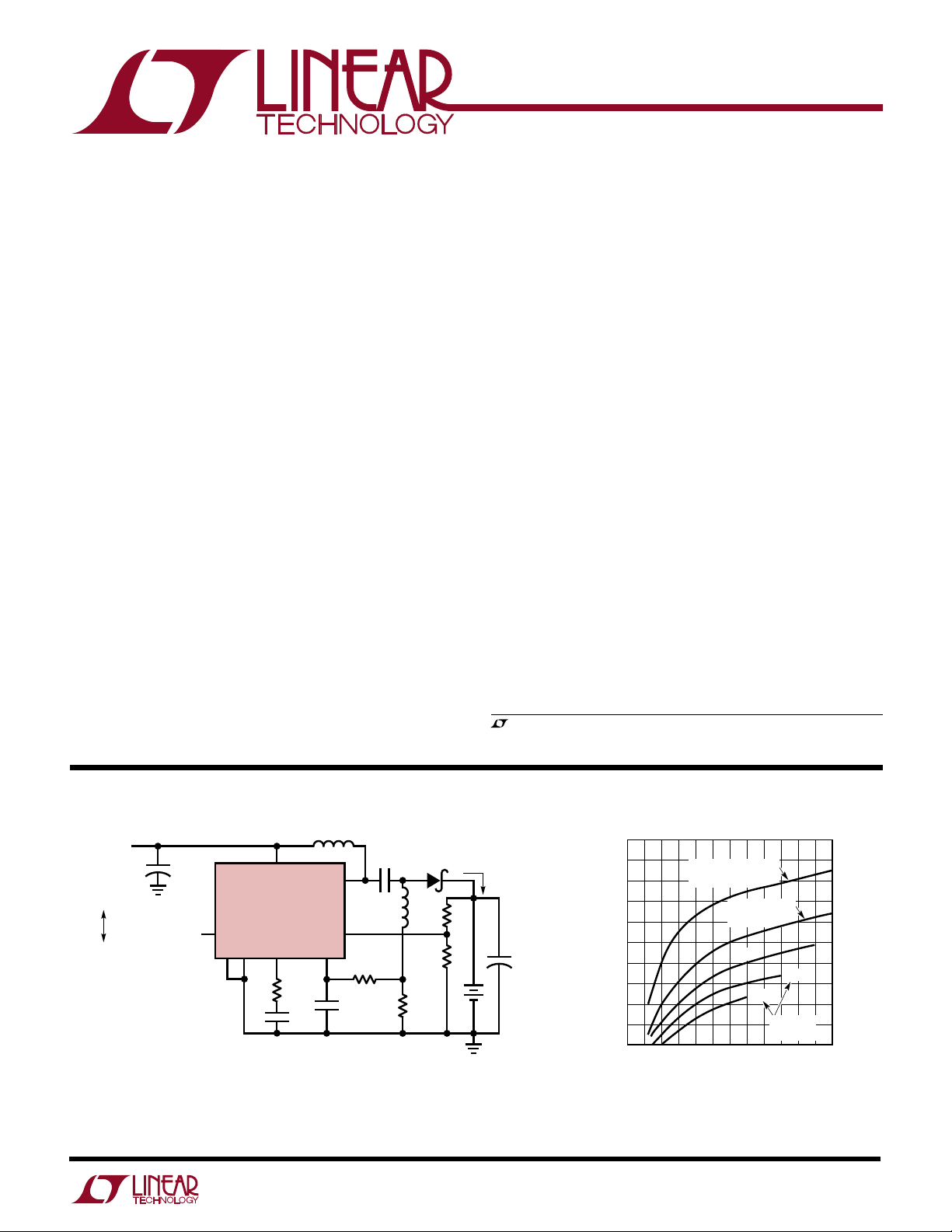
TYPICAL APPLICATION
WALL
ADAPTER
INPUT
CHARGE
SHUTDOWN
C3
+
22µF
25V
SYNC
AND/OR
SHUTDOWN
6
**
LT1513
S/S
GND
TAB4
*
L1A, L1B ARE TWO 10µH WINDINGS ON A
COMMON CORE: COILTRONICS CTX10-4
CERAMIC MARCON THCR40EIE475Z OR TOKIN 1E475ZY5U-C304
†
MBRD340 OR MBRS340T3. MBRD340 HAS 5µA TYPICAL
LEAKAGE, MBRS340T3 50µA TYPICAL
Figure 1. SEPIC Charger with 1.25A Output Current
•
7
V
IN
V
C
13
R5
270Ω
C5
0.1µF
U
L1A*
V
V
I
FB
SW
5
2
FB
C4
0.22µF
R4
39Ω
C2**
4.7µF
†
D1
L1B*
•
R3
0.08Ω
Maximum Charging Current
2.4
2.2
1.25A
R1
C1
+
R2
LT1513 • TA01
22µF
25V
× 2
2.0
1.8
1.6
1.4
1.2
CURRENT (A)
1.0
0.8
0.6
0.4
05
INDUCTOR = 10µH
ACTUAL PROGRAMMED CHARGING CURRENT WILL BE
INDEPENDENT OF INPUT VOLTAGE IF IT DOES NOT
EXCEED VALUES SHOWN
SINGLE Li-Ion CELL
(4.1V)
DOUBLE Li-Ion
CELL (8.2V)
12V
20V
10
INPUT VOLTAGE (V)
20
15
16V
BATTERY
VOLTAGE
25
LT1513 • TA02
30
1
Page 2
LT1513/LT1513-2
A
W
O
LUTEXI T
S
A
WUW
ARB
U
G
I
S
Supply Voltage ....................................................... 30V
Switch Voltage........................................................ 40V
S/S Pin Voltage....................................................... 30V
FB Pin Voltage (Transient, 10ms) ......................... ±10V
VFB Pin Current .................................................... 10mA
IFB Pin Voltage (Transient, 10ms)......................... ±10V
/
PACKAGE
TAB
IS
GND
7-LEAD PLASTIC DD
WITH PACKAGE SOLDERED TO 0.5INCH
AREA OVER BACKSIDE GROUND PLANE OR INTERNAL
POWER PLANE, θ
> 40°C/W DEPENDING ON MOUNTING TECHNIQUE
O
RDER I FOR ATIO
FRONT VIEW
7
6
5
4
3
2
1
R PACKAGE
T
= 125°C, θ
JMAX
JA
JA
CAN VARY FROM 20°C/W TO
= 30°C/W
2
COPPER
VIN
S/S
V
SW
GND
I
FB
FB
V
C
WU
ORDER PART
NUMBER
LT1513CR
LT1513CR-2
LT1513IR
LT1513IR-2
U
Operating Junction Temperature Range
LT1513C............................................... 0°C to 125°C
LT1513I ............................................ –40°C to 125°C
Short Circuit ......................................... 0°C to 150°C
Storage Temperature Range ................ –65°C to 150°C
Lead Temperature (Soldering, 10 sec)................. 300°C
ORDER PART
NUMBER
FRONT VIEW
V
IN
S/S
V
SW
GND
I
FB
FB
V
C
LT1513CT7-2
LT1513IT7-2
T
JMAX
T7 PACKAGE
7-LEAD TO-220
= 125°C, θ
7
6
5
4
3
2
1
= 50°C/ W, θJC = 4°C/W
JA
Consult factory for Military grade parts.
LECTRICAL C CHARA TERIST
E
VIN = 5V, VC = 0.6V, VFB = V
SYMBOL PARAMETER CONDITIONS MIN TYP MAX UNITS
V
REF
V
IREF
I
FBVOS
g
m
FB Reference Voltage Measured at FB Pin 1.233 1.245 1.257 V
FB Input Current VFB = V
FB Reference Voltage Line Regulation 2.7V ≤ VIN ≤ 25V, VC = 0.8V ● 0.01 0.03 %/V
IFB Reference Voltage (LT1513) Measured at IFB Pin –107 –100 – 93 mV
IFB Input Current V
IFB Reference Voltage Line Regulation 2.7V ≤ VIN ≤ 25V, VC = 0.8V ● 0.01 0.05 %/V
IFB Voltage Offset (LT1513-2) (Note 3) I
IFB Input Current V
VFB Source Current V
Error Amplifier Transconductance ∆IC = ±25µA 1100 1500 1900 µmho
Error Amplifier Source Current VFB = V
Error Amplifier Sink Current VFB = V
, IFB = 0V, VSW and S/S pins open, unless otherwise noted.
REF
ICS
VC = 0.8V ● 1.228 1.245 1.262 V
REF
VFB = 0V, VC = 0.8V ● –110 –100 –90 mV
= V
IFB
VFB
IFB
IREF
(Note 2) ● 10 25 35 µA
IREF
= 60µA (Note 4) ● –7.5 2.5 12.5 mV
= V
IREF
= –10mV, VFB = 1.2V ● – 700 –300 – 100 µA
– 150mV, VC = 1.5V ● 120 200 350 µA
REF
+ 150mV, VC = 1.5V ● 1400 2400 µA
REF
● 600 nA
● – 200 – 10 0 nA
● 700 2300 µmho
300 550 nA
2
Page 3
LT1513/LT1513-2
LECTRICAL C CHARA TERIST
E
VIN = 5V, VC = 0.6V, VFB = V
SYMBOL PARAMETER CONDITIONS MIN TYP MAX UNITS
Error Amplifier Clamp Voltage High Clamp, VFB = 1V 1.70 1.95 2.30 V
A
V
f Switching Frequency 2.7V ≤ VIN ≤ 25V 450 500 550 kHz
BV Output Switch Breakdown Voltage 0°C ≤ TJ ≤ 125°C4047V
Error Amplifier Voltage Gain 500 V/V
VC Pin Threshold Duty Cycle = 0% 0.8 1 1.25 V
Maximum Switch Duty Cycle ● 85 95 %
Switch Current Limit Blanking Time 130 260 ns
, IFB = 0V, VSW and S/S pins open, unless otherwise noted.
REF
ICS
Low Clamp, VFB = 1.5V 0.25 0.40 0.52 V
0°C ≤ TJ ≤ 125°C 430 500 580 kHz
T
< 0°C 400 580 kHz
J
T
< 0°C35V
J
V
SAT
I
LIM
∆IIN/∆ISWSupply Current Increase During Switch ON Time 15 25 mA/A
I
Q
The ● denotes specifications which apply over the full operating
temperature range.
Note 1: For duty cycles (DC) between 50% and 85%, minimum
guaranteed switch current is given by I
Output Switch ON Resistance ISW = 2A ● 0.25 0.45 Ω
Switch Current Limit Duty Cycle = 50% ● 3.0 3.8 5.4 A
Control Voltage to Switch Current 4A/V
Transconductance
Minimum Input Voltage ● 2.4 2.7 V
Supply Current 2.7V ≤ VIN ≤ 25V ● 4 5.5 mA
Shutdown Supply Current 2.7V ≤ VIN ≤ 25V, V
Shutdown Threshold 2.7V ≤ VIN ≤ 25V ● 0.6 1.3 2 V
Shutdown Delay ● 51225µs
S/S Pin Input Current 0V ≤ V
Synchronization Frequency Range ● 600 800 kHz
= 1.33 (2.75 – DC).
LIM
Duty Cycle = 80% (Note 1)
≤ 0.6V, TJ ≥ 0°C ● 12 30 µA
TJ < 0°C50µA
≤ 5V ● –10 15 µA
S/S
S/S
Note 2: The I
Note 3: Consult factory for grade selected parts.
Note 4: The I
pin is servoed to its regulating state with VC = 0.8V.
FB
pin is sevoed to regulate FB to 1.245V
FB
● 2.6 3.4 5.0 A
3
Page 4
LT1513/LT1513-2
TEMPERATURE (°C)
–50
1.8
INPUT VOLTAGE (V)
2.0
2.2
2.4
2.6
050
100
150
LT1513 • G03
2.8
3.0
–25 25
75
125
W
U
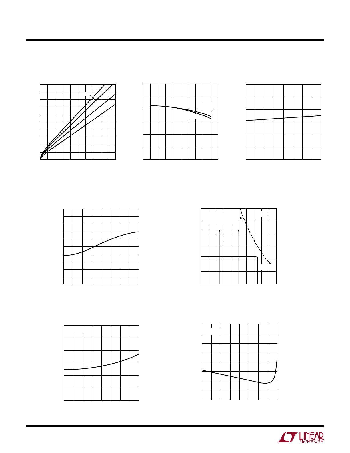
TYPICAL PERFORMANCE CHARACTERISTICS
Switch Saturation Voltage
vs Switch Current
1.0
0.9
0.8
0.7
0.6
0.5
0.4
0.3
0.2
SWITCH SATURATION VOLTAGE (V)
0.1
0
0.8
0.4
0
1.2
SWITCH CURRENT (A)
1.6
100°C
2.0
Negative Feedback Input Current
vs Temperature
0
–10
–20
–30
–40
NEGATIVE FEEDBACK INPUT CURRENT (µA)
–50
–50
–25 25
0
150°C
25°C
–55°C
2.4
2.8
3.2
3.6
LT1513 • G01
50
TEMPERATURE (°C)
Minimum Input Voltage
vs Temperature
4.0
Switch Current Limit
vs Duty Cycle
6
5
4
3
2
SWITCH CURRENT LIMIT (A)
1
0
20 40 60 80
DUTY CYCLE (%)
–55°C
25°C AND
125°C
LT1513 • G02
10010030 50 70 90
Output Charging Characteristics
Showing Constant-Current and
Constant-Voltage Operation
12
CHARGING CURRENT
10
WITH 12V INPUT
8
6
4
BATTERY VOLTAGE (V)
2
125
100
75
150
LT1513 • G06
0
(A) (B)
0.4 0.8 1.2 1.6
CHARGING CURRENT (A)
V
= 12VMAXIMUM AVAILABLE
IN
(A) 8.4V BATTERY
= 0.5A
I
CHRG
(B) 8.4V BATTERY
I
= 1A
CHRG
(C) 4.2V BATTERY
I
= 1.5A
(C)
1513 G07
CHRG
2.00.200.6 1.0 1.4 1.8
4
Minimum Peak-to-Peak
Synchronization Voltage vs Temperature
)
3.0
P-P
2.5
2.0
1.5
1.0
0.5
MINIMUM SYNCHRONIZATION VOLTAGE (V
0
–50
f
= 700kHz
SYNC
050
–25 25
TEMPERATURE (°C)
75
100
125
LT1513 • G04
150
Feedback Input Current
vs Temperature
800
VFB = V
–25
REF
0
50
25
TEMPERATURE (°C)
700
600
500
400
300
200
FEEDBACK INPUT CURRENT (nA)
100
0
–50
75
100
125
LT1513 • G05
150
Page 5

UUU
PIN FUNCTIONS
V
(Pin 1): The compensation pin is primarily used for
C
frequency compensation, but it can also be used for soft
starting and current limiting. It is the output of the error
amplifier and the input of the current comparator. Peak
switch current increases from 0A to 3.6A as the VC voltage
varies from 1V to 1.9V. Current out of the VC pin is about
200µ A when the pin is externally clamped below the
internal 1.9V clamp level. Loop frequency compensation
is performed with a capacitor or series RC network from
the VC pin
FB (Pin 2): The feedback pin is used for positive output
voltage sensing. The R1/R2 voltage divider connected to
FB defines Li-Ion float voltage at full charge, or acts as a
voltage limiter for NiCd or NiMH applications. FB is the
inverting input to the voltage error amplifier. Input bias
current is typically 300nA, so divider current is normally
set to 100µ A to swamp out any output voltage errors due
to bias current. The noninverting input of this amplifier is
tied internally to a 1.245V reference. The grounded end of
the output voltage divider should be connected directly to
the LT1513 ground pin (avoid ground loops).
I
FB
charging current. It is the input to a current sense amplifier
that controls charging current when the battery voltage is
below a programmed limit. During constant-current
operation, the LT1513 IFB pin regulates at –100mV. Input
resistance of this pin is 5kΩ, so filter resistance (R4,
Figure 1) should be less than 50Ω. The 39Ω, 0.22µ F filter
shown in Figure 1 is used to convert the pulsating current
in the sense resistor to a smooth DC current feedback
signal. The LT1513-2 IFB pin regulates at 0mV to provide
programmable current limit. The current through R5,
Figure 5, is balanced by the current through R4, programming the maximum voltage across R3.
directly to the ground pin
(Pin 3): The current feedback pin is used to sense
(avoid ground loops).
LT1513/LT1513-2
GND (Pin 4): The ground pin is common to both control
circuitry and switch current. VC, FB and S/S signals must
be Kelvin and connected as close as possible to this pin.
The TAB of the R package should also be connected to the
power ground.
V
(Pin 5): The switch pin is the collector of the power
SW
switch, carrying up to 3A of current with fast rise and fall
times. Keep the traces on this pin as short as possible to
minimize radiation and voltage spikes. In particular, the
path in Figure 1 which includes SW to C2, D1, C1 and
around to the LT1513 ground pin should be as short as
possible to minimize voltage spikes at switch turn-off.
S/S (Pin 6): This pin can be used for shutdown and/or
synchronization. It is logic level compatible, but can be
tied to VIN if desired. It defaults to a high ON state when
floated. A logic low state will shut down the charger to a
micropower state. Driving the S/S pin with a continuous
logic signal of 600kHz to 800kHz will synchronize switching frequency to the external signal. Shutdown is avoided
in this mode with an internal timer.
VIN (Pin 7): The input supply pin should be bypassed with
a low ESR capacitor located right next to the IC chip. The
grounded end of the capacitor must be connected directly
to the ground plane to which the TAB is connected.
TAB: The TAB on the surface mount R package is electrically connected to the ground pin, but a low inductance
connection must be made to both the TAB and the pin for
proper circuit operation. See suggested PC layout in
Figure 4.
5
Page 6

LT1513/LT1513-2
BLOCK DIAGRAM
W
V
IN
S/S
4k
I
FB
50k*
V
FB
1.245V
REF
SHUTDOWN
DELAY AND RESET
SYNC
+
–
–
–
+
*REMOVE ON LT1513-2
500kHz
OSC
I
FBA
EA
LOW DROPOUT
2.3V REG
LOGIC DRIVER
COMP
IA
≈ 6
A
V
C
Figure 2
V
ANTISAT
+
–
SW
SWITCH
0.04Ω
LT1513 • BD
U
OPERATION
The LT1513 is a current mode switcher. This means that
switch duty cycle is directly controlled by switch current
rather than by output voltage or current. Referring to the
Block Diagram, the switch is turned “on” at the start of each
oscillator cycle. It is turned “off” when switch current
reaches a predetermined level. Control of output voltage
and current is obtained by using the output of a dual
feedback voltage sensing error amplifier to set switch
current trip level. This technique has the advantage of
simplified loop frequency compensation. A low dropout
internal regulator provides a 2.3V supply for all internal
circuitry on the LT1513. This low dropout design allows
input voltage to vary from 2.7V to 25V. A 500kHz oscillator
is the basic clock for all internal timing. It turns “on” the
output switch via the logic and driver circuitry. Special
adaptive antisat circuitry detects onset of saturation in the
power switch and adjusts driver current instantaneously to
limit switch saturation. This minimizes driver dissipation
and provides very rapid turn-off of the switch.
A unique error amplifier design has two inverting inputs
which allow for sensing both output voltage and current. A
1.245V bandgap reference biases the noninverting input.
The first inverting input of the error amplifier is brought out
for positive output voltage sensing. The second inverting
input is driven by a “current” amplifier which is sensing
output current via an external current sense resistor. The
current amplifier is set to a fixed gain of –12.5 which
provides a –100mV current limit sense voltage.
The LT1513-2 option removes the feedback resistors
around the IFB amplifier and connects its output to the FB
signal. This provides a ground referenced current sense
voltage suitable for external current programming and
makes amplifier input and output available for external
loop compensation.
The error signal developed at the amplifier output is
brought out externally and is used for frequency compensation. During normal regulator operation this pin sits at a
voltage between 1V (low output current) and 1.9V (high
output current). Switch duty cycle goes to zero if the VC pin
is pulled below the VC pin threshold, placing the LT1513 in
an idle mode.
6
Page 7

LT1513/LT1513-2
LT1513
V
IN
L1A
L1B
GND
V
FB
1513 F03
V
SW
ADAPTER
INPUT
C2
SCHEMATIC SIMPLIFIED FOR CLARITY
D2 = 1N914, 1N4148 OR EQUIVALENT
C6
470pF
R6
470k
R3
R1
R2
D2
D1
C1
+
U
WUU
APPLICATIONS INFORMATION
The LT1513 is an IC battery charger chip specifically optimized to use the SEPIC converter topology. A complete
charger schematic is shown in Figure 1. The SEPIC topology
has unique advantages for battery charging. It will operate
with input voltages above, equal to or below the battery
voltage, has no path for battery discharge when turned off,
and eliminates the snubber losses of flyback designs. It also
has a current sense point that is ground referred and need
not be connected directly to the battery. The two inductors
shown are actually just two identical windings on one
inductor core, although two separate inductors can be used.
A current sense voltage is generated with respect to ground
across R3 in Figure 1. The average current through R3 is
always identical to the current delivered to the battery. The
LT1513 current limit loop will servo the voltage across R3
to –100mV when the battery voltage is below the voltage
limit set by the output divider R1/R2. Constant-current
charging is therefore set at 100mV/R3. R4 and C4 filter the
current signal to deliver a smooth feedback voltage to the I
pin. R1 and R2 form a divider for battery voltage sensing and
set the battery float voltage. The suggested value for R2 is
12.4k. R1 is calculated from:
RV
2 1 245
(–.)
R
1
=
V
BAT
BAT
1 245 2 0 3
.(.)
RA
+µ
= battery float voltage
0.3µ A = typical FB pin bias current
A value of 12.4k for R2 sets divider current at 100µ A. This is
a constant drain on the battery when power to the charger is
off. If this drain is too high, R2 can be increased to 41.2k,
reducing divider current to 30µA. This introduces an addi-
tional uncorrectable error to the constant voltage float mode
of about ±0.5% as calculated by:
±µ
V Error =
BAT
0.15 A(R1)(R2)
1.245(R1+R2)
FB
Figure 3. D2, C6 and R6 form a peak detector to drive the gate
of the FET to about the same as the battery voltage. If power
is turned off, the gate will drop to 0V and the only drain on the
battery will be the reverse leakage of the catch diode D1. See
Diode Selection for a discussion of diode leakage.
Figure 3. Eliminating Divider Current
Maximum Input Voltage
Maximum input voltage for the LT1513 is partly determined
by battery voltage. A SEPIC converter has a maximum
switch voltage equal to input voltage plus output voltage.
The LT1513 has a maximum input voltage of 30V and a
maximum switch voltage of 40V, so this limits maximum
input voltage to 30V, or 40V – V
, whichever is less.
BAT
Shutdown and Synchronization
The dual function S/S pin provides easy shutdown and
synchronization. It is logic level compatible and can be
pulled high or left floating for normal operation. A logic low
on the S/S pin activates shutdown, reducing input supply
current to 12µ A. To synchronize switching, drive the S/S pin
between 600kHz and 800kHz.
Inductor Selection
±0.15µA = expected variation in FB bias current around the
nominal 0.3µ A typical value.
With R2 = 41.2k and R1 = 228k, (V
to variations in bias current would be ±0.42%.
A second option is to disconnect the divider when charger
power is off. This can be done with a small NFET as shown in
= 8.2V), the error due
BAT
L1A and L1B are normally just two identical windings on one
core, although two separate inductors can be used. A typical
value is 10µ H, which gives about 0.5A peak-to-peak inductor current. Lower values will give higher ripple current,
which reduces maximum charging current. 5µ H can be used
if charging currents are at least 20% lower than the values
7
Page 8

LT1513/LT1513-2
U
WUU
APPLICATIONS INFORMATION
shown in the maximum charging current graph. Higher
inductance values give slightly higher maximum charging
current, but are larger and more expensive. A low loss toroid
core such as Kool Mµ®, Molypermalloy or Metglas® is
recommended. Series resistance should be less than 0.04Ω
for each winding. “Open core” inductors, such as rods or
barrels are not recommended because they generate large
magnetic fields which may interfere with other electronics
close to the charger.
Input Capacitor
The SEPIC topology has relatively low input ripple current
compared to other topologies and higher harmonics are
especially low. RMS ripple current in the input capacitor is
less than 0.25A with L = 10µH and less than 0.5A with
L = 5µ H. A low ESR 22µ F, 25V solid tantalum capacitor (AVX
type TPS or Sprague type 593D) is adequate for most
applications with the following caveat. Solid tantalum
capacitors can be destroyed with a very high turn-on surge
current such as would be generated if a low impedance input
source were “hot switched” to the charger input. If this
condition can occur, the input capacitor should have the
highest possible voltage rating, at least twice the surge input
voltage if possible. Consult with the capacitor manufacturer
before a final choice is made. A 4.7µ F ceramic capacitor such
as the one used for the coupling capacitor can also be used.
These capacitors do not have a turn-on surge limitation. The
input capacitor must be connected directly to the VIN pin and
the ground plane close to the LT1513.
in Figure 1. These are AVX type TPS or Sprague type 593D
surface mount solid tantalum units intended for switching
applications. Do not substitute other types without ensuring
that they have adequate ripple current ratings. See Input
Capacitor section for details of surge limitation on solid
tantalum capacitors if the battery may be “hot switched” to
the output of the charger.
Coupling Capacitor
C2 in Figure 1 is the coupling capacitor that allows a SEPIC
converter topology to work with input voltages either higher
or lower than the battery voltage. DC bias on the capacitor is
equal to input voltage. RMS ripple current in the coupling
capacitor has a maximum value of about 1A at full charging
current. A conservative formula to calculate this is:
IVV
()(.)
I
COUP RMS
()
(1.1 is a fudge factor to account for inductor ripple current
and other losses)
With I
The recommended capacitor is a 4.7µF ceramic type from
Marcon or Tokin. These capacitors have extremely low ESR
and high ripple current ratings in a small package. Solid
tantalum units can be substituted if their ripple current rating
is adequate, but typical values will increase to 22µ F or more
to meet the ripple current requirements.
= 1.2A, VIN = 15V and V
CHRG
CHRG IN BAT
=
+ 11
V
()
2
IN
BAT
= 8.2V, I
COUP
= 1.02A.
Output Capacitor
It is assumed as a worst case that all the switching output
ripple current from the battery charger could flow in the
output capacitor. This is a desirable situation if it is necessary to have very low switching ripple current in the battery
itself. Ferrite beads or line chokes are often inserted in series
with the battery leads to eliminate high frequency currents
that could create EMI problems. This forces all the ripple
current into the output capacitor. Total RMS current into the
capacitor has a maximum value of about 1A, and this is
handled with the two paralleled 22µ F, 25V capacitors shown
Kool Mµ is a registered trademark of Magnetics, Inc.
Metglas is a registered trademark of AlliedSignal Inc.
8
Diode Selection
The switching diode should be a Schottky type to minimize
both forward and reverse recovery losses. Average diode
current is the same as output charging current, so this will be
under 2A. A 3A diode is recommended for most applications,
although smaller devices could be used at reduced charging
current.
Maximum diode reverse voltage will be equal to
input voltage plus battery voltage.
Diode reverse leakage current will be of some concern
during charger shutdown. This leakage current is a direct
drain on the battery when the charger is not powered. High
Page 9

LT1513/LT1513-2
U
WUU
APPLICATIONS INFORMATION
current Schottky diodes have relatively high leakage currents (5µ A to 500µA) even at room temperature. The latest
very-low-forward devices have especially high leakage currents. It has been noted that surface mount versions of some
Schottky diodes have as much as ten times the leakage of
their through-hole counterparts. This may be because a low
forward voltage process is used to reduce power dissipation
in the surface mount package. In any case, check leakage
specifications carefully before making a final choice for the
switching diode. Be aware that diode manufacturers want
to specify a maximum leakage current that is ten times
higher than the typical leakage. It is very difficult to get them
to specify a low leakage current in high volume production.
This is an on going problem for all battery charger circuits
and most customers have to settle for a diode whose typical
leakage is adequate, but theoretically has a worst-case
condition of higher than desired battery drain.
Thermal Considerations
Care should be taken to ensure that worst-case conditions
do not cause excessive die temperatures. Typical thermal
resistance is 30°C/W for the R package but this number will
vary depending on the mounting technique (copper area,
airflow, etc.).
Average supply current (including driver current) is:
ImA
=+4
IN
VI
BAT CHRG
V
IN
0 024()( )(.)
Switch power dissipation is given by:
2
CHRG SW BAT IN BAT
V
()
+()()( )()
2
IN
P
SW
IRVVV
=
RSW = Output switch ON resistance
Total power dissipation of the die is equal to supply current
times supply voltage, plus switch power:
P
D(TOTAL)
For VIN = 10V, V
= (IIN)(VIN) + P
= 8.2V, I
BAT
SW
= 1.2A, RSW = 0.3Ω,
CHRG
IIN = 4mA + 24mA = 28mA
PSW = 0.64W
PD = (10)(0.028) + 0.64 = 0.92W
GROUND PLANE
++
LT1513 TAB AND GROUND
PIN SOLDERED TO
GROUND PLANE
C5
R5
C1,C3,C5 AND R3
R3
TIED DIRECTLY TO
GROUND PLANE
Figure 4. LT1513 Suggested Partial Layout for Critical Thermal and Electrical Paths
C3
C1 C1
L1A L1B
+
V
C2
2 WINDING
INDUCTOR
V
IN
BAT
D1
LT1513 • F04
9
Page 10

LT1513/LT1513-2
U
WUU
APPLICATIONS INFORMATION
Programmed Charging Current
LT1513-2 charging current can be programmed with a DC
voltage source or equivalent PWM signal, as shown in
Figure 5. In constant-current mode, IFB acts as a virtual
ground. The I
voltage across R4 in the ratio R4/R5.
Charging current is given by:
I
CHARGE
IFB input current is small and can normally be ignored, but
IFB offset voltage must be considered if operating over a
wide range of program currents. The voltage across R3 at
maximum charge current can be increased to reduce
offset errors at lower charge currents. In Figure 5, I
from 0V to 5V corresponds to an I
+37/–62mA. C4 and R4 smooth the switch current waveform. During constant-current operation, the voltage feedback network loads the FB pin, which is held at V
IFB amplifier. It is recommended that this load does not
voltage across R5 is balanced by the
SET
VRRI
()(/)–45
ISET FBVOS
=
R
3
CHARGE
of 0A to 1A
REF
SET
by the
exceed 60µA to maintain a sharp constant voltage to
constant current crossover characteristic. I
CHARGE
can
also be controlled by a PWM input. Assuming the signal is
a CMOS rail-to-rail output with a source impedance of less
than a few hundred ohms, effective I
by the PWM ratio. I
CHARGE
has good linearity over the
is VCC multiplied
SET
entire 0% to 100% range.
Voltage Mode Loop Stability
The LT1513 operates in constant-voltage mode during the
final phase of charging lithium-ion and lead-acid batteries.
This feedback loop is stabilized with a series resistor and
capacitor on the VC pin of the chip. Figure 6 shows the
simplified model for the voltage loop. The error amplifier is
modeled as a transconductance stage with gm = 1500µ mho
LT1513-2
I
FB
R5
249k
I
SET
R4
10k
C4
0.1µF
L1B
R3
0.2Ω
1513 F05
MODULATOR SECTION
I
V14(VIN)
V1
**
C
P
3pF
RP**
V
C
R5
330Ω
C5
0.1µF
* FOR 8.4V BATTERY. ADJUST VALUE OF R1 FOR ACTUAL BATTERY VOLTAGE
** R
P
THIS IS A SIMPLIFIED AC MODEL FOR THE LT1513 IN CONSTANTVOLTAGE MODE. RESISTOR AND CAPACITOR NUMBERS
CORRESPOND TO THOSE USED IN FIGURE 1. R
THE PHASE DELAY IN THE MODULATOR. C3 IS 3pF FOR A 10µH
INDUCTOR. IT SHOULD BE SCALED PROPORTIONALLY FOR OTHER
INDUCTOR VALUES (6pF FOR 20µH). THE MODULATOR IS A
TRANSCONDUCTANCE WHOSE GAIN IS A FUNCTION OF INPUT AND
BATTERY VOLTAGE AS SHOWN.
1M
RG
330k
AND CP MODEL PHASE DELAY IN THE MODULATOR
P
g
= =
m
V
= DC INPUT VOLTAGE
IN
V
BAT
+ V
V
IN
= DC BATTERY VOLTAGE
–
EA
+
g
m
1500µmho
BAT
1.245V
AND CP MODEL
P
I
Figure 6. Constant-Voltage Small-Signal Model
Figure 5
P
R1*
71.5k
FB
+
R2
12.5k
AS SHOWN, THIS LOOP HAS A UNITY-GAIN FREQUENCY OF
ABOUT 250Hz. UNITY-GAIN WILL MOVE OUT TO SEVERAL
KILOHERTZ IF BATTERY RESISTANCE INCREASES TO SEVERAL
OHMS. R5 IS NOT USED IN ALL APPLICATIONS, BUT IT GIVES
BETTER PHASE MARGIN IN CONSTANT-VOLTAGE MODE WITH
HIGH BATTERY RESISTANCE.
C1C1
R
CAP
≈0.15Ω
EACH
+
C1
22µF
EACH
R
BAT
0.1Ω
BATTERY
1513 F06
10
Page 11

LT1513/LT1513-2
U
WUU
APPLICATIONS INFORMATION
(from the Electrical Characteristics). Amplifier output resistance is modeled with a 330k resistor. The power stage
(modulator section) of the LT1513 is modeled as a transconductance whose value is 4(VIN)/(VIN + V
simplified model of the actual power stage, but it is sufficient
when the unity-gain frequency of the loop is low compared
to the switching frequency. The output filter capacitor model
includes its ESR (R
). A series resistance (R
CAP
assigned to the battery model.
Analysis of this loop normally shows an extremely stable
system for all conditions, even with 0Ω for R5. The one
condition which can cause reduced phase margin is with a
very large battery resistance (>5Ω), or with the battery
replaced with a resistive load. The addition of R5 gives good
phase margin even under these unusual conditions. R5
should not be increased above 330Ω without checking for
two possible problems. The first is instability in the constant
current region (see Constant-Current Mode Loop Stability),
and the second is subharmonic switching where switch duty
cycle varies from cycle to cycle. This duty cycle instability is
caused by excess switching frequency ripple voltage on the
VC pin. Normally this ripple is very low because of the
filtering effect of C5, but large values of R5 can allow high
ripple on the VC pin. Normal loop analysis does not show this
). This is a very
BAT
) is also
BAT
problem, and indeed small signal loop stability can be
excellent even in the presence of subharmonic switching.
The primary issue with subharmonics is the presence of EMI
at frequencies below 500kHz.
Constant-Current Mode Loop Stability
The LT1513 is normally very stable when operating in constant-current mode (see Figure 7), but there are certain conditions which may create instabilities. The combination of
higher value current sense resistors (low programmed charging current), higher input voltages, and the addition of a loop
compensation resistor (R5) on the VC pin may create an unstable current mode loop. (A resistor is sometimes added in
series with C5 to improve loop phase margin when the loop
is operating in voltage mode.) Instability results
because loop gain is too high in the 50kHz to 150kHz region
where excess phase occurs in the current sensing amplifier
and the modulator. The I
amplifier (gain of –12.5) has a
FBA
pole at approximately 150kHz. The modulator section consisting of the current comparator, the power switch and the
magnetics, has a pole at approximately 50kHz when the
coupled inductor value is 10µH. Higher inductance will reduce
the pole frequency proportionally. The design procedure presented here is to roll off the loop to unity-gain at a frequency
of 25kHz or lower to avoid these excess phase regions.
V1
MODULATOR SECTION
C
RP**
FB
V
C
R5
330Ω
C5
0.1µF
THIS IS A SIMPLIFIED AC MODEL FOR THE LT1513 IN
CONSTANT-CURRENT MODE. RESISTOR AND CAPACITOR
NUMBERS CORRESPOND TO THOSE USED IN FIGURE 1.
AND CP MODEL THE PHASE DELAY IN THE PowerPath.
R
P
C3 IS 3pF FOR A 10µH INDUCTOR. IT SHOULD BE SCALED
PROPORTIONALLY FOR OTHER INDUCTOR VALUES (6pF
FOR 20µH). THE PowerPath IS A TRANSCONDUCTANCE
WHOSE GAIN IS A FUNCTION OF INPUT AND BATTERY
VOLTAGE AS SHOWN.
1M
R
G
330k
P
3pF
EA
g
m
1500µmho
–
+
I
=
P
1.245V
4(V1)(V
V
IN
Figure 7. Constant-Current Small-Signal Model
I
P
)
IN
+ V
BAT
R
A
100k
C
A
10pF
THE CURRENT AMPLIFIER HAS A FIXED VOLTAGE GAIN OF 12.
ITS PHASE DELAY IS MODELED WITH R
THE ERROR AMPLIFIER HAS A TRANSCONDUCTANCE OF
1500µmho AND AN INTERNAL OUTPUT SHUNT RESISTANCE OF
330k.
AS SHOWN, THIS LOOP HAS A UNITY-GAIN FREQUENCY OF
ABOUT 27kHz. R5 IS NOT USED IN ALL APPLICATIONS, BUT IT
GIVES BETTER PHASE MARGIN IN CONSTANT VOLTAGE MODE.
VOLTAGE
GAIN = 12
–
I
FBA
+
I
FB
AND CA.
A
R4
24Ω
C4
0.22µF
R3
0.1Ω
1513 F07
11
Page 12

LT1513/LT1513-2
U
WUU
APPLICATIONS INFORMATION
The suggested way to control unity loop frequency is to
increase the filter time constant on the IFB pin (R4/C4 in
Figures 1 and 7). The filter resistor cannot be arbitrarily
increased because high values will affect charging current
accuracy. Charging current will increase by 1% for each
40Ω increase in R4. There is no inherent limitation on the
value of C4, but if this capacitor is ceramic, it should be an
X7R type to maintain its value over temperature. X7R
dielectric requires a larger footprint.
The formula for calculating the minimum value for the filter
capacitor C4 is:
RV R
3 4 12 1500 5
()()()()( )()
C
4
=
VIN = Highest input voltage
1500µ = Transconductance of error amplifier
(EA)f = Desired unity-gain frequency
V
= Battery voltage
BAT
IN
fR V V
24
()( )( )
π
IN BAT
µ
+
For example, assume V
current set to 0.25A), R4 = 24Ω, R5 = 330Ω and V
0 4 4 15 12 0 0015 330
CF4
The value for C4 could be reduced to a more manageable size
by increasing R4 to 75Ω and reducing R5 to 300Ω, yielding
0.47µ F for C4. The 2% increase in charging current can be
ignored or factored into the value for R3.
More Help
Linear Technology Field Application Engineers have a CAD
spreadsheet program for detailed calculations of circuit
operating conditions. In addition, our Applications Department is always ready to lend a helping hand. The LT1371
data sheet may also be helpful. The LT1513 is identical
except for the current amplifier circuitry.
. ( )( )( )( . )( )
IN(MAX)
= 15V, R3 = 0.4Ω (charging
= 8V,
BAT
=
15 81=+
)6.3(25000)(39)(
µ
12
Page 13

U
TYPICAL APPLICATIONS
LT1513/LT1513-2
Lithium-Ion Battery Charger with
Switchable Charge Current
Many battery chemistries require several constant-current
settings during the charging cycle. The circuit shown in
Figure 8 uses the LT1513-2 to provide switchable 1.35A and
0.13A constant-current modes. The circuit is based on a
standard SEPIC battery charger circuit set to a single
lithium-ion cell charge voltage of 4.1V. The LT1513-2 has I
FB
referenced to ground allowing a simple resistor network to
set the charging current values. In constant-current mode,
the IFB error amplifier drives the FB pin, increasing charging
current, until IR4 is balanced by IR5.
L1A
V
IN
CHARGE
SHUTDOWN
PRECHARGE
CHARGE
3.3V
R6
10k
R7
910Ω
Q1
+
C3
25µF
25V
R3
330Ω
C5
0.1µF
CTX10-4
•
7
V
IN
6
S/S
LT1513-2
1
V
C
GND
V
SW
V
I
4
R5
36k
I
CHARGE
()()–
=
4
5
R FBVOS
R
3
IRI
There are several ways to control IR5 including DAC, PWM or
resistor network as shown here. If the lithium cell requires
precharging, Q1 is turned on, setting a constant current of
0.13A. When charge voltage is reached, Q1 is turned off,
programming the full charge current of 1.35A. As the cell
voltage approaches 4.1V, the voltage sensing network (R1,
R2) starts driving the VFB pin, changing the LT1513-2 to
constant-voltage mode. As charging current falls, the output
remains in constant-voltage mode for the remainder of the
charging cycle. When charging is complete, the LT1513-2
can be shut down with the S/S pin.
C2
4.7µF
5
2
FB
3
FB
R4
4.7k
C4
0.22µF
D1
MBRS330T3
L1B
•
R3
0.25Ω
R1
78.7k
0.5%
R2
34k
0.5%
+
Li-Ion
RECHARGABLE
CELL
C1
22µF
25V
×2
GND
1513 F08
Figure 8. Lithium-Ion Battery Charger
13
Page 14

LT1513/LT1513-2
U
TYPICAL APPLICATIONS
This Cold Cathode Fluorescent Lamp driver uses a Royer
class self-oscillating sine wave converter to driver a high
voltage lamp with an AC waveform. CCFL Royer converters
have significantly degraded efficiency if they must operate at
low input voltages, and this circuit was designed to handle
input voltages as low as 2.7V. Therefore, the LT1513 is
connected to generate a negative current through L2 that
allows the Royer to operate as if it were connected to a
constant higher voltage input.
2.7V
C1
TO 20V
C10
10nF
47µF
ELECT
+
V
6
S/S
2
V
FB
V
7
IN
C
1
D2
15V
C9
1µF
R7
2k
L1
20µH
LT1513-2
V
GND
R4
20k
C5
4.7nF
SW
5
I
FB
4, TAB
R3
3
C6
0.1µF
10k
R5
330k
The Royer output winding and the bulb are allowed to float in
this circuit. This can yield significantly higher efficiency in
situations where the stray bulb capacitance to surrounding
enclosure is high. To regulate bulb current in Figure 9, Royer
input
current is sensed with R2 and filtered with R3 and C6.
This negative feedback signal is applied to the IFB pin of the
LT1513. For more information on this circuit contact the LTC
Applications Department and see Design Note 133. Considerable written application literature on Royer CCFL circuits is
also available from other LTC Application and Design Notes.
R2
0.25Ω
12
•
Q1
5
NEGATIVE VOLTAGE
IS GENERATED HERE
T1
•
10
LAMP CURRENT
6
C4
27pF
3kV
CCFL
5.6mA
C2
4.7µF
CERAMIC
L2
20µH
D1
3A
Q2
C3
0.082µF
WIMA
3
•
4
R1
470Ω
14
PWM DIMMING
(≈1kHz)
C2: TOKIN MULTILAYER CERAMIC
C3: MUST BE A LOW LOSS CAPACITOR, WIMA MKP-20 OR EQUIVALENT
L1, L2: COILTRONICS CTX20-4 (MUST BE SEPARATE INDUCTORS)
Q1, Q2: ZETEX ZTX849 OR FZT849
T1: COILTRONICS CTX110605 (67:1)
Figure 9. CCFL Power Supply for Floaing Lamp Configuration Operates on 2.7V
1513 F09
Page 15

PACKAGE DESCRIPTION
LT1513/LT1513-2
U
Dimensions in inches (millimeters) unless otherwise noted.
R Package
7-Lead Plastic DD Pak
(LTC DWG # 05-08-1462)
0.256
(6.502)
0.060
(1.524)
0.300
(7.620)
BOTTOM VIEW OF DD PAK
HATCHED AREA IS SOLDER PLATED
COPPER HEAT SINK
0.060
(1.524)
0.075
(1.905)
0.183
(4.648)
0.060
(1.524)
TYP
0.330 – 0.370
(8.382 – 9.398)
+0.012
0.143
–0.020
+0.305
3.632
()
–0.508
0.026 – 0.036
(0.660 – 0.914)
0.390 – 0.415
(9.906 – 10.541)
15° TYP
0.040 – 0.060
(1.016 – 1.524)
0.165 – 0.180
(4.191 – 4.572)
T7 Package
7-Lead Plastic TO-220 (Standard)
(LTC DWG # 05-08-1422)
0.059
(1.499)
TYP
0.013 – 0.023
(0.330 – 0.584)
0.045 – 0.055
(1.143 – 1.397)
+0.008
0.004
–0.004
+0.203
0.102
()
–0.102
0.095 – 0.115
(2.413 – 2.921)
0.050 ± 0.012
(1.270 ± 0.305)
R (DD7) 0396
0.390 – 0.415
(9.906 – 10.541)
0.460 – 0.500
(11.684 – 12.700)
0.040 – 0.060
(1.016 – 1.524)
0.147 – 0.155
(3.734 – 3.937)
DIA
0.230 – 0.270
(5.842 – 6.858)
0.570 – 0.620
(14.478 – 15.748)
0.330 – 0.370
(8.382 – 9.398)
0.152 – 0.202
0.260 – 0.320
(6.604 – 8.128)
0.026 – 0.036
(0.660 – 0.914)
Information furnished by Linear Technology Corporation is believed to be accurate and reliable.
However, no responsibility is assumed for its use. Linear Technology Corporation makes no representation that the interconnection of its circuits as described herein will not infringe on existing patent rights.
(3.860 – 5.130)
0.165 – 0.180
(4.191 – 4.572)
0.700 – 0.728
(17.780 – 18.491)
0.135 – 0.165
(3.429 – 4.191)
0.620
(15.75)
TYP
0.045 – 0.055
(1.143 – 1.397)
0.095 – 0.115
(2.413 – 2.921)
0.013 – 0.023
(0.330 – 0.584)
0.155 – 0.195
(3.937 – 4.953)
T7 (TO-220) (FORMED) 1197
15
Page 16

LT1513/LT1513-2
RELATED PARTS
PART NUMBER DESCRIPTION COMMENTS
LT1239 Backup Battery Management System Charges Backup Battery and Regulates Backup Battery Output when
Main Battery Removed
LTC®1325 Microprocessor Controlled Battery Management System Can Charge, Discharge and Gas Gauge NiCd, NiMH and Pb-Acid Batteries
with Software Charging Profiles
LT1510 1.5A Constant-Current/Constant-Voltage Battery Charger Step-Down Charger for Li-Ion, NiCd and NiMH
LT1511 3.0A Constant-Current/Constant-Voltage Battery Charger Step-Down Charger that Allows Charging During Computer Operation and
with Input Current Limiting Prevents Wall-Adapter Overload
LT1512 SEPIC Constant-Current/Constant-Voltage Battery Charger Step-Up/Step-Down Charger for Up to 1A Current
16
Linear Technology Corporation
1630 McCarthy Blvd., Milpitas, CA 95035-7417 ● (408) 432-1900
FAX: (408) 434-0507
●
TELEX: 499-3977 ● www.linear-tech.com
1513fa LT/TP 0198 REV A 4K • PRINTED IN THE USA
LINEAR TE CHNOLO GY CORPOR ATION 1 996
 Loading...