

Page 1
FEATURES
LT1507
500kHz Monolithic
Buck Mode Switching Regulator
■
Constant 500kHz Switching Frequency
■
Uses All Surface Mount Components
■
Operates with Inputs as Low as 4V
■
Saturated Switch Design (0.3Ω)
■
Cycle-by-Cycle Current Limiting
■
Easily Synchronizable
■
Inductor Size as Low as 2µH
■
Shutdown Current: 20µA
U
APPLICATIONS
■
Portable Computers
■
Battery-Powered Systems
■
Battery Charger
■
Distributed Power
U
DESCRIPTION
The LT®1507 is a 500kHz monolithic buck mode switching
regulator, functionally identical to the LT1375 but optimized for lower input voltage applications. It will operate
over a 4V to 15V input range, compared with 5.5V to 25V
for the LT1375. A 1.5A switch is included on the die along
with all the necessary oscillator, control and logic circuitry. High switching frequency allows a considerable
reduction in the size of external components. The topology
is current mode for fast transient response and good loop
stability. Both fixed output voltage (3.3V) and adjustable
parts are available.
A special high speed bipolar process and new design
techniques allow this regulator to achieve high efficiency
at a high switching frequency. Efficiency is maintained
over a wide output current range by keeping quiescent
supply current to 4mA and by utilizing a supply boost
capacitor to allow the NPN power switch to saturate. A
shutdown signal will reduce supply current to 20µA. The
LT1507 can be externally synchronized from 570kHz to
1MHz with logic level inputs.
The LT1507 fits into standard 8-pin SO and PDIP packages. Temperature rise is kept to a minimum by the high
efficiency design. Full cycle-by-cycle short-circuit protection and thermal shutdown are provided. Standard surface
mount external parts are used including the inductor and
capacitors.
, LTC and LT are registered trademarks of Linear Technology Corporation.
U
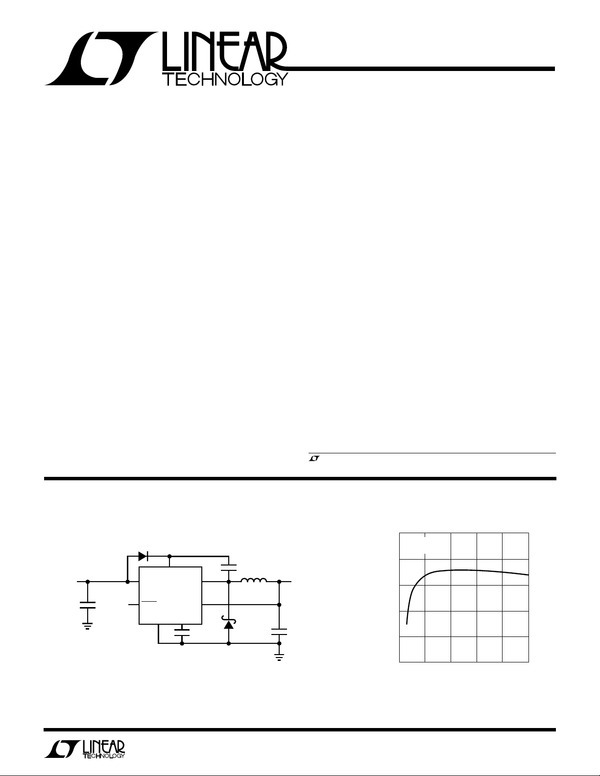
TYPICAL APPLICATION
5V to 3.3V Volt Down Converter
D2†
1N914
BOOST
= ON
V
IN
SHDN
GND V
LT1507-3.3
V
SW
SENSE
C
CC
3.3nF
5V
C3*
47µF
16V
TANTALUM
AVX TPSD477M016R0150 OR SPRAGUE 593D EQUIVALENT.
*
RIPPLE CURRENT RATING ≥ 0.6A
AVX TPSD108M010R0100 OR SPRAGUE 593D EQUIVALENT
**
COILTRONICS CTX5-1. SUBSTITUTION UNITS SHOULD BE RATED
***
AT ≥ 1.25A, USING LOW LOSS CORE MATERIAL
†
SEE BOOST PIN CONSIDERATIONS IN APPLICATIONS INFORMATION
SECTION FOR ALTERNATIVE D2 CONNECTION
+
DEFAULT
(OPEN)
C2
0.1µF
L1***
5µH
D1
1N5818
OUTPUT
3.3V
1.25A
C1**
+
100µF
10V
TANTALUM
100
VIN = 5V
V
OUT
90
80
70
EFFICIENCY (%)
60
50
0
5V to 3.3V Efficiency
= 3.3V
0.25
LOAD CURRENT (A)
0.50
0.75
1.00
1.25
LT1507 • TA02
1
Page 2
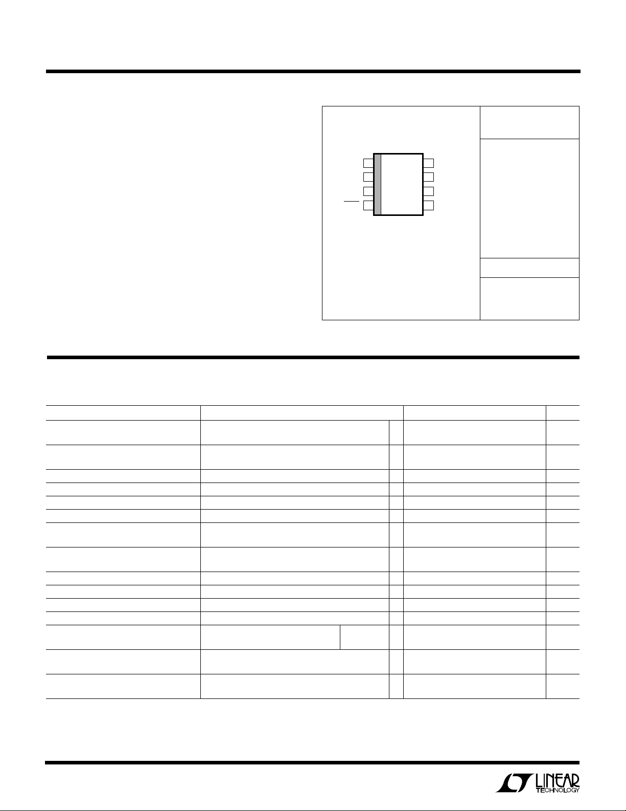
LT1507
1
2
3
4
8
7
6
5
TOP VIEW
V
C
FB/SENSE
GND
SYNC
BOOST
V
IN
V
SW
SHDN
N8 PACKAGE
8-LEAD PDIP
S8 PACKAGE
8-LEAD PLASTIC SO
WW
W
U
ABSOLUTE MAXIMUM RATINGS
Input Voltage ........................................................... 16V
Boost Pin Voltage .................................................... 25V
Shutdown Pin Voltage ............................................... 7V
FB Pin Voltage (Adjustable Part)............................. 3.5V
FB Pin Current (Adjustable Part)............................. 1mA
Sense Voltage (Fixed 3.3V Part) ................................ 5V
Sync Pin Voltage ....................................................... 7V
Operating Ambient Temperature Range
LT1507C.................................................. 0°C to 70°C
LT1507I .............................................. –40°C to 85°C
Max Operating Junction Temperature................... 125°C
Storage Temperature Range ................. –65°C to 150°C
Lead Temperature (Soldering, 10 sec)..................300°C
U
W
PACKAGE/ORDER INFORMATION
ORDER PART
NUMBER
LT1507CN8
LT1507CN8-3.3
LT1507CS8
LT1507CS8-3.3
LT1507IN8
LT1507IN8-3.3
LT1507IS8
LT1507IS8-3.3
T
= 125°C, θJA = 80°C/W TO 120°C/ W (N)
JMAX
= 125°C, θJA = 120°C/W TO 170°C/ W (S)
T
JMAX
DEPENDING ON PC BOARD LAYOUT
Consult factory for Military grade parts.
S8 PART MARKING
1507
15073
1507I
1507I3
U
ELECTRICAL CHARACTERISTICS
TJ = 25°C, VIN = 5V, VC = 1.5V, boost open, switch open unless otherwise specified.
PARAMETER CONDITIONS MIN TYP MAX UNITS
Reference Voltage (Adjustable) 2.39 2.42 2.45 V
All Conditions ● 2.36 2.48 V
Sense Voltage (3.3V) 3.25 3.3 3.35 V
All Conditions ● 3.23 3.37 V
Sense Pin Resistance ● 4.0 6.6 9.5 kΩ
Reference Voltage Line Regulation 4.3V ≤ VIN ≤ 15V ● 0.01 0.03 %/V
FB Input Bias Current ● 0.5 2 µA
Error Amplifier Voltage Gain (Note 8) (Note 1) 150 400
Error Amplifier Transconductance (Note 8) ∆I(V
Pin to Switch Current
V
C
Transconductance 2 A/V
Error Amplifier Source Current VFB = 2.1V or V
Error Amplifier Sink Current VFB = 2.7V or V
VC Pin Switching Threshold Duty Cycle = 0 0.9 V
VC Pin High Clamp VFB = 2.1V or V
Switch Current Limit VC Open, VFB = 2.1V or V
Switch On Resistance (Note 6) ISW = 1.5A, V
Maximum Switch Duty Cycle VFB = 2.1V or V
) = ±10µA 1500 2000 2700 µmho
C
VIN ≥ 5V, V
= 2.9V ● 150 225 320 µA
SENSE
= 3.7V 2 mA
SENSE
= 2.9V 2.1 V
SENSE
= 2.9V DC ≤ 50% ● 1.50 2 3 A
SENSE
= VIN + 5V DC = 80% ● 1.35 3 A
BOOST
= VIN + 5V 0.3 0.4 Ω
BOOST
= 2.9V 90 93 %
SENSE
● 1100 3000 µmho
● 0.5 Ω
● 86 93 %
2
Page 3
LT1507
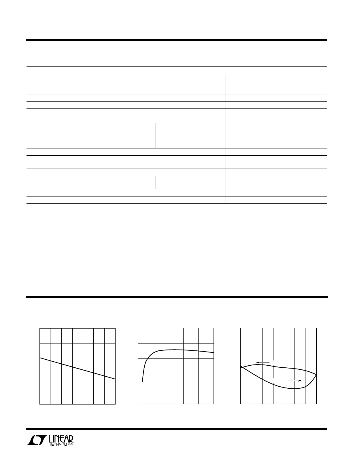
JUNCTION TEMPERATURE (°C)
–50
2.44
2.43
2.42
2.41
2.40
100
LT1507 • TPC03
–25 0 25 50 75 125
FEEDBACK VOLTAGE (V)
CURRENT (µA)
2.0
1.5
1.0
0.5
0
VOLTAGE
CURRENT
ELECTRICAL CHARACTERISTICS
TJ = 25°C, VIN = 5V, VC = 1.5V, boost open, switch open unless otherwise specified.
PARAMETER CONDITIONS MIN TYP MAX UNITS
Switch Frequency VC Set to Give 50% Duty Cycle 460 500 540 kHz
–25°C ≤ T
TJ ≤ –25°C 440 570 kHz
Switch Frequency Line Regulation 4.3V ≤ VIN ≤ 15V ● 0.05 0.15 %/V
Frequency Shifting Threshold on FB Pin ∆f = 10kHz ● 0.8 1.0 1.3 V
Minimum Input Voltage (Note 2) ● 4 4.3 V
Minimum Boost Voltage (Note 3) ISW ≤ 1.5A ● 3 3.5 V
Boost Current (Note 4) V
BOOST
Input Supply Current (Note 5) ● 3.8 5.4 mA
Shutdown Supply Current V
SHDN
VSW = 0V, VC Open ● 75 µA
Lockout Threshold VC Open ● 2.3 2.38 2.46 V
Shutdown Threshold V
C
Minimum Synchronizing Amplitude ● 1.5 2.2 V
Synchronizing Frequency Range (Note 7) 580 1000 kHz
≤ 125°C 440 560 kHz
J
= VIN + 5V ISW = 500mA, –25°C ≤ TJ ≤ 125°C1222mA
T
≤ –25°C25mA
I
= 1.5A, –25°C ≤ TJ ≤ 125°C2535mA
SW
J
T
≤ –25°C40mA
J
= 0V, VIN ≤ 12V 15 50 µA
Open Device Shutting Down ● 0.15 0.37 0.70 V
Device Starting Up ● 0.25 0.45 0.70 V
● denotes specifications which apply over the operating temperature
The
range.
Note 1: Gain is measured with a V
clamp level to 200mV below the upper clamp level.
Note 2: Minimum input voltage is not measured directly, but is guaranteed
by other tests. It is defined as the voltage where internal bias lines are still
regulated, so that the reference voltage and oscillator frequency remain
constant. Actual minimum input voltage to maintain a regulated output will
depend on output voltage and load current. See Applications Information.
Note 3: This is the minimum voltage across the boost capacitor needed to
guarantee full saturation of the internal power switch.
Note 4: Boost current is the current flowing into the BOOST pin with the
pin held 5V above input voltage. It flows only during switch ON time.
TYPICAL PERFORMANCE CHARACTERISTICS
1.4
1.2
1.0
0.8
THRESHOLD VOLTAGE (V)
0.6
0.4
C
VC Pin Shutdown Threshold
–25 0 25 50 75 125
–50
JUNCTION TEMPERATURE (°C)
swing equal to 200mV above the low
W
U
Switch Peak Current Limit Feedback Pin Voltage and Current
100
VIN = 5V
= 3.3V
V
OUT
90
100
LT1507 • TPC01
80
70
EFFICIENCY (%)
60
50
0
0.25
0.50
LOAD CURRENT (A)
Note 5: Input supply current is the bias current drawn by the V
pin when
IN
the SHDN pin is held at 1V (switching disabled).
Note 6: Switch ON resistance is calculated by dividing V
to VSW voltage
IN
by the forced current (1.5A). See Typical Performance Characteristics for
the graph of switch voltage at other currents.
Note 7: For synchronizing frequency above 700kHz, with duty cycles
above 50%, external slope compensation may be needed. See Applications
Information.
Note 8: Transconductance and voltage gain refer to the internal amplifier
exclusive of the voltage divider. To calculate gain and transconductance
refer to SENSE pin on fixed voltage parts. Divide values shown by the ratio
/2.42.
V
OUT
0.75
1.00
1.25
LT1507 • TA02
3
Page 4
LT1507
INPUT VOLTAGE (V)
0
0
INPUT SUPPLY CURRENT (µA)
5
10
15
20
25
30
36912
LT1507 • TPC06
15
V
SHDN
= 0V
FREQUENCY (Hz)
GAIN (µmho)
PHASE (DEG)
3000
2500
2000
1500
1000
500
200
150
100
50
0
–50
100 10k 100k 10M
LT1507 • TPC09
1k 1M
GAIN
PHASE
R
OUT
200k
C
OUT
12pF
V
C
V
FB
× 2e
–3
ERROR AMPLIFIER EQUIVALENT CIRCUIT
R
LOAD
= 50Ω
LOAD CURRENT (mA)
1
5.0
INPUT VOLTAGE (V)
5.5
6.0
6.5
10 100 1000
LT1507 • TPC12
4.5
4.0
3.5
3.0
MINIMUM VOLTAGE
TO START WITH
STANDARD CIRCUIT
MINIMUM VOLTAGE
TO RUN WITH
STANDARD CIRCUIT
MINIMUM INPUT VOLTAGE CAN BE REDUCED
BY ADDING A SMALL EXTERNAL PNP. SEE
APPLICATIONS INFORMATION
W
U
TYPICAL PERFORMANCE CHARACTERISTICS
Shutdown Pin Bias Current
500
CURRENT REQUIRED TO FORCE SHUTDOWN
(FLOWS OUT OF PIN). AFTER SHUTDOWN,
400
CURRENT DROPS TO A FEW µA
300
200
CURRENT (µA)
8
AT 2.38V STANDBY THRESHOLD
(CURRENT FLOWS OUT OF PIN)
4
0
–50
–25 0
25 75
TEMPERATURE (°C)
50 100 125
L11507 • TPC04
Standby and Shutdown Thresholds
2.40
STANDBY
2.36
2.32
0.8
STARTUP
0.4
SHUTDOWN PIN VOLTAGE (V)
0
–50
–25 0
SHUTDOWN
50 100 125
25 75
JUNCTION TEMPERATURE (°C)
Shutdown Supply Current Error Amplifier Transconductance
150
125
100
75
50
INPUT SUPPLY CURRENT (µA)
25
VIN = 10V
2500
2000
1500
1000
500
TRANSCONDUCTANCE (µmho)
Shutdown Supply Current
LT1507 • TPC05
Error Amplifier Transconductance
0
0.1 0.2 0.3 0.4
0
SHUTDOWN VOLTAGE (V)
Frequency Foldback
500
400
300
200
100
0
SWITCHING FREQUENCY (kHz) OR CURRENT (µA)
0
4
SWITCHING
FREQUENCY
FEEDBACK PIN
CURRENT
0.5
1.0
FEEDBACK PIN VOLTAGE (V)
LT1507 • TPC07
0.5
0
–50
0
–25
JUNCTION TEMPERATURE (°C)
50
25
75
100
LT1507 • TPC08
125
Minimum Input Voltage
with 3.3V OutputSwitching Frequency
600
550
500
2.0
LT1507 • TPC10
2.5
1.5
FREQUENCY (kHz)
450
400
–25 0 25 50 75 125
–50
JUNCTION TEMPERATURE (°C)
100
LT1507 • TPC11
Page 5
W
INPUT VOLTAGE (V)
0
0
CURRENT (A)
0.25
0.50
0.75
1.00
1.25
1.50
36912
LT1507 • TPC15
15
L = 10µH
L = 5µH
L = 20µH
U
TYPICAL PERFORMANCE CHARACTERISTICS
LT1507
Current Limit Foldback
2.5
2.0
1.5
1.0
OUTPUT CURRENT (A)
0.5
*POSSIBLE
UNDESIRED
STABLE POINT
FOR CURRENT
SOURCE LOAD
0
20
0
OUTPUT VOLTAGE (%)
*SEE "MORE THAN JUST VOLTAGE FEEDBACK"
IN APPLICATIONS INFORMATION SECTION
FOLDBACK
CHARACTERISTICS
60
40
RESISTOR LOAD
Boost Pin Current
12
TJ = 25°C
10
8
CURRENT
SOURCE LOAD
MOS LOAD
80
LT1507 • TPC13
100
Maximum Load Current
at V
= 3.3V
1.50
1.25
1.00
0.75
CURRENT (A)
0.50
0.25
OUT
V
L = 10µH
L = 5µH
L = 3µH
L = 2µH
0
4
6 8 10 12
INPUT VOLTAGE (V)
Inductor Core Loss for 3.3V Output
1.0
V
= 3.3V
OUT
= 5V
V
IN
= 1A
I
OUT
0.1
TYPE 52 POWDERED IRON
OUT
= 3.3V
LT1507 • TPC14
Maximum Load Current
at V
= 5V
OUT
14
Switch Voltage Drop
0.8
TJ = 25°C
0.6
6
4
BOOST PIN CURRENT (mA)
2
0
0.25 0.50 0.75 1.00
0
Kool Mµ is a registered trademark of Magnetics, Incorporated.
Metglas is a registered trademark of AlliedSignal Incorporated.
SWITCH CURRENT (A)
1.25
LT1507 • TPC16
CORE LOSS (W)
0.01
PERMALLOY
0.001
1
CORE LOSS IS INDEPENDENT OF LOAD CURRENT
UNTIL LOAD CURRENT FALLS LOW ENOUGH
FOR CIRCUIT TO GO INTO DISCONTINUOUS MODE
®
Kool Mµ
µ = 125
246810
INDUCTANCE (µH)
UUU
PIN FUNCTIONS
BOOST (Pin 1): The BOOST pin is used to provide a drive
voltage, higher than the input voltage, to the internal
bipolar NPN power switch. Without this added voltage the
typical switch voltage loss would be about 1.5V. The
additional boost voltage allows the switch to saturate and
voltage loss approximates that of a 0.3Ω FET structure,
but with a much smaller die area. Efficiency improves from
0.4
SWITCH VOLTAGE (V)
0.2
0
0.25 0.50 0.75 1.00
0
SWITCH CURRENT (A)
1.25 1.50
LT1507 • TPC18
Metglas
®
LT1507 • TPC17
70% for conventional bipolar designs to greater than 85%
for these new parts.
VIN (Pin 2): Input Pin. The LT1507 is designed to operate
with an input voltage between 4.5V and 15V. Under certain
conditions, input voltage may be reduced down to 4V.
Actual minimum operating voltage will always be higher
than the output voltage. It may be limited by switch
5
Page 6

LT1507
PIN FUNCTIONS
UUU
saturation voltage and maximum duty cycle. A typical
value for minimum input voltage is 1V above output
voltage. Start-up conditions may require more voltage at
light loads. See Minimum Input Voltage for details.
VSW (Pin 3): The switch pin is driven up to the input voltage
in the ON state and is an open circuit in the OFF state. At
higher load currents, pin voltage during the off condition
will be one diode drop below ground as set by the external
catch diode. At lighter loads the pin will assume an
intermediate state equal to output voltage during part of
the switch OFF time. Maximum
switch pin is 1V with respect to the GND pin, so it must
always be clamped with a catch diode to the GND pin.
SHDN (Pin 4): The shutdown pin is used to turn off the
regulator and to reduce input drain current to a few
microamperes. Actually this pin has two separate thresholds, one at 2.38V to disable switching and a second at
0.4V to force complete micropower shutdown. The 2.38V
threshold functions as an accurate undervoltage lockout
(UVLO). This is sometimes used to prevent the regulator
from delivering power until the input voltage has reached
a predetermined level.
negative
voltage on the
SYNC (Pin 5): The SYNC pin is used to synchronize the
internal oscillator to an external signal. It is directly logic
compatible and can be driven with any signal between
10% and 90% duty cycle. The synchronizing range is
equal to
Sychronizing section for details.
FB/SENSE (Pin 7): The feedback pin is used to set output
voltage using an external voltage divider that generates
2.42V at the pin with the desired output voltage. The fixed
voltage (– 3 .3V) parts have the divider included on the chip
and the feedback pin is used as a sense pin connected
directly to the 5V output. Two additional functions are
performed by the feedback pin. When the pin voltage
drops below 1.7V, switch current limit is reduced. Below
1V, switching frequency is also reduced. See More Than
Just Voltage Feedback.
VC (Pin 8): The VC pin is the output of the error amplifier
and the input of the peak switch current comparator. It is
normally used for frequency compensation but can do
double duty as a current clamp or control loop override.
This pin sets at about 1V for very light loads and 2V at
maximum load. It can be driven to ground to shut off the
regulator, but if driven high, current must be limited to 4mA.
initial
operating frequency up to 1MHz. See
W
BLOCK DIAGRAM
The LT1507 is a constant frequency, current mode buck
converter. This means that there is an internal clock and
two feedback loops that control the duty cycle of the power
switch. In addition to the normal error amplifier, there is
a current sense amplifier that monitors switch current on
a cycle-by-cycle basis. A switch cycle starts with an
oscillator pulse which sets the RS flip-flop to turn the
switch on. When switch current reaches a level set by the
inverting input of the comparator, the flip-flop is reset and
the switch turns off. Output voltage control is obtained by
using the output of the error amplifier to set the switch
current trip point. This technique means that the error
amplifier commands current to be delivered to the output
rather than voltage. A voltage fed system will have low
phase shift up to the resonant frequency of the inductor
and output capacitor, then an abrupt 180° shift will occur.
The current fed system will have 90° phase shift at a much
lower frequency, but will not have the additional 90° shift
until well beyond the LC resonant frequency. This makes
it much easier to frequency compensate the feedback loop
and also gives much quicker transient response.
High switch efficiency is attained by using the BOOST pin
to provide a voltage to the switch driver which is higher
than the input voltage, allowing the switch to be saturated.
This boosted voltage is generated with an external capacitor and diode.
Two comparators are connected to the shutdown pin. One
has a 2.38V threshold for undervoltage lockout and the
second has a 0.4V threshold for complete shutdown.
6
Page 7

BLOCK DIAGRAM
LT1507
W
V
BIAS
SYNC
SHDN
IN
2
5
SHUTDOWN
COMPARATOR
4
2.9V BIAS
REGULATOR
+
0.4V
3.5µA
+
–
2.38V
–
LOCKOUT
COMPARATOR
INTERNAL
V
CC
SLOPE COMP
500kHz
OSCILLATOR
0.1Ω
+
–
CURRENT
SENSE
AMPLIFIER
VOLTAGE GAIN = 5
BOOST
Σ
8
0.9V
+
–
FOLDBACK
CURRENT
LIMIT
CLAMP
V
C
CURRENT
COMPARATOR
Q2
S
R
S
FLIP-FLOP
R
FREQUENCY
SHIFT CIRCUIT
ERROR
AMPLIFIER
g
= 2000µmho
m
DRIVER
CIRCUITRY
–
+
2.42V
1
Q1
POWER
SWITCH
V
3
SW
7
FB/SENSE
Figure 1. Block Diagram
U
WUU
APPLICATIONS INFORMATION
Note: This application section is adapted from the more
complete version found in the LT1375/LT1376 data sheet.
If more details are desired consult the LT1375/LT1376
Applications Information section, but please acquaint
yourself thoroughly with this LT1507 information first so
that differences between the LT1375 and the LT1507 do
not cause confusion.
6
GND
LT1507 • BD
FEEDBACK PIN FUNCTIONS
The feedback pin (FB or SENSE) on the LT1507 is used to
set output voltage and also to provide several overload
protection features. The first part of this section deals with
selecting resistors to set output voltage and the remaining
part talks about foldback frequency and current limiting
created by the FB pin. Please read both parts before
7
Page 8

LT1507
U
WUU
APPLICATIONS INFORMATION
committing to a final design. The fixed 3.3V LT1507-3.3
has internal divider resistors and the FB pin is renamed
SENSE, connected directly to the output.
The suggested value for the output divider resistor from FB
to ground (R2) is 5k or less and the formula for R1 is
shown below. The output voltage error caused by ignoring
the input bias current on the FB pin is less than 0.25% with
R2 = 5k. Please read below if R2 is increased above the
suggested value.
R2(V – 2.42)
R1
=
More Than Just Voltage Feedback
The feedback pin is used for more than just output voltage
sensing. It also reduces switching frequency and current
limit when output voltage is very low (see graph in Typical
Performance Characteristics). This is done to control
power dissipation in both the IC and in the external diode
and inductor during short-circuit conditions. A shorted
output requires the switching regulator to operate at very
low duty cycles and the average current through the diode
and inductor is equal to the short-circuit current limit of the
switch (typically 2A of the LT1507, folding back to less
than 1A). Minimum switch ON time limitations would
prevent the switcher from attaining a sufficiently low duty
cycle if switching frequency were maintained at 500kHz,
so frequency is reduced by about 5:1 when the feedback
OUT
2.42
pin voltage drops below 1V (see Frequency Foldback
graph). This does not affect operation with normal load
conditions; one simply sees a gear shift in switching
frequency during start-up as the output voltage rises.
In addition to lower switching frequency, the LT1507 also
operates at lower switch current limit when the feedback
pin voltage drops below 1.5V. This
foldback current limit
greatly reduces power dissipation in the IC, diode and
inductor during short-circuit conditions. Again, it is nearly
transparent to the user under normal load conditions. The
only loads which may be affected are current source loads
which maintain full-load current with output voltage less
than 50% of final value. In these rare situations, the
feedback pin can be clamped above 1.5V with an external
diode to defeat foldback current limit.
Caution
: clamping
the feedback pin means that frequency shifting will also be
defeated, so a combination of high input voltage and dead
shorted output may cause the LT1507 to lose control of
current limit.
The internal circuitry which forces reduced switching
frequency also causes current to flow out of the feedback
pin when output voltage is low. If the FB pin falls below 1V,
current begins to flow out of the pin and reduces frequency
at the rate of approximately 5kHz/µ A. To ensure adequate
frequency foldback (under worst-case short-circuit conditions) the external divider Thevinin resistance must be
low enough to pull 150µ A out of the FB pin with 0.6V on the
8
BOOST
= ON
V
IN
SHDN
GND V
V
IN
C3*
33µF
20V
TANTALUM
AVX TPSD337M020R0200 OR SPRAGUE 593 EQUIVALENT.
*
RIPPLE CURRENT RATING ≥ 0.6A
AVX TPSD108M010R0100 OR SPRAGUE 593 EQUIVALENT
**
COILTRONICS CTX5-1. SUBSTITUTION UNITS SHOULD BE RATED
***
AT ≥ 1.25A, USING LOW LOSS CORE MATERIAL. LOAD CURRENTS
ABOVE 0.85A MAY NEED A 10µH OR 20µH INDUCTOR
+
DEFAULT
(OPEN)
Figure 2. Typical Schematic for LT1507 Adjustable Application
LT1507
V
SW
FB
C
CC
3.3nF
D2
1N914
C2
0.1µF
L1***
5µH
D1
1N5818
R1
5.36k
R2
4.99k
OUTPUT
5V
C1**
+
100µF
10V
TANTALUM
LT1507 • F01
Page 9

LT1507
U
WUU
APPLICATIONS INFORMATION
pin (R
in frequency and current limit are affected by output
voltage divider impedance. Although divider impedance is
not critical, caution should be used if resistors are
increased beyond the suggested values and short-circuit
conditions will occur with high input voltage.
frequency pickup will also increase and the protection
accorded by frequency and current foldback will decrease.
CHOOSING THE INDUCTOR AND OUTPUT CAPACITOR
For most applications the value of the inductor will fall in
the range of 2µH to 10µH. Lower values are chosen to
reduce physical size of the inductor. Higher values allow
more output current because they reduce peak current
seen by the LT1507 switch, which has a 1.5A limit. Higher
values also reduce output ripple voltage and reduce core
loss. Graphs in the Typical Performance Characteristics
section show maximum output load current versus inductor size and input voltage. A second graph shows core loss
versus inductor size for various core materials.
When choosing an inductor you might have to consider
maximum load current, core and copper losses, allowable
component height, output voltage ripple, EMI, fault current in the inductor, saturation and, of course, cost. The
following procedure is suggested as a way of handling
these somewhat complicated and conflicting requirements.
1. Choose a value in microhenries from the graphs of
= R1/R2 ≤ 4k).
DIV
Maximum Load Current and Inductor Core Loss for
3.3V Output. If you want to double check that the
chosen inductor
go to the next section, Maximum Output Load Current.
Choosing a small inductor with lighter loads may result
in discontinuous mode of operation, but the LT1507 is
designed to work well in either mode. Keep in mind that
lower core loss means higher cost, at least for closedcore geometries like toroids. Type 52 powdered iron,
Kool Mµ and Molypermalloy are old standbys for tor-
oids in ascending order of price. A newcomer, Metglas,
gives very low core loss with high saturation current.
Assume that the average inductor current is equal to
load current and decide whether or not the inductor
must withstand continuous fault conditions. If maximum load current is 0.5A, for instance, a 0.5A inductor
The net result is that reductions
value
will allow sufficient load current,
High
may not survive a continuous 1.5A overload condition.
Dead shorts (V
the inductor because the LT1507 has foldback current
limiting (see graph in Typical Performance Characteristics).
2. Calculate peak inductor current at full load current to
ensure that the inductor will not saturate. Peak current
can be significantly higher than output current, especially with smaller inductors and lighter loads, so don’t
omit this step. Powdered iron cores are forgiving
because they saturate softly, whereas ferrite cores
saturate abruptly. Other core materials fall in between
somewhere. The following formula assumes a continuous mode of operation, but it errs only slightly on
the high side for discontinuous mode, so it can be used
for all conditions.
II
=+
PEAK OUT
VIN = Maximum input voltage
f = Switching frequency = 500kHz
3. Decide if the design can tolerate an “open” core geom-
etry like ferrite rods or barrels, which have high magnetic field radiation or whether it needs a closed core
like a toroid to prevent EMI problems. One would not
want an open core next to a magnetic storage media for
instance! This is a tough decision because the rods or
barrels are temptingly cheap and small and there are no
helpful guidelines to calculate when the magnetic field
radiation will be a problem. The following is an example
of just how subtle the “B” field problems can be with
open geometry cores.
We had selected an open drum shaped ferrite core for
the LTC1376 demonstration board because the inductor was extremely small and inexpensive. It met all the
requirements for current and the ferrite core gave low
core loss. When the boards came back from assembly,
many of them had somewhat higher than expected
output ripple voltage. We removed the inductors and
output capacitors and found them to be no different
than the good boards. After much head scratching and
hours of delicate low level ripple measurements on the
good and bad boards, I realized that the problem must
≤ 1V) will actually be more gentle on
OUT
VVV
(– )
OUT IN OUT
fLV
()()( )2
IN
9
Page 10

LT1507
U
WUU
APPLICATIONS INFORMATION
be due to a radiated magnetic field coupling into PC
board traces. But why were some boards bad and
others good? In a moment of desperation (or divine
inspiration) I unsoldered a “bad” inductor, rotated it
180° and resoldered it. Problem fixed!!
It turns out that the inductor was symmetrical in all
regards except that the polarity of the magnetic field
reversed when the unit was rotated 180° because
current flowed in the opposite direction in the coil. In
one direction, the magnetically induced ripple in the
board traces
tor caused the induced field to
Unfortunately the inductor had no physical package
assymmetry to indicate rotation, including part marking, so we had to visually examine the winding in each
unit before soldering it to the boards. This little horror
story should not preclude the use of open core inductors, but it emphasizes the need to carefully check the
effect these seductively small, low cost inductors may
have on regulator or system performances.
added
to output ripple. Rotating the induc-
reduce
output ripple.
Table 1. Representative Surface Mount Units
VALUE DC CORE SERIES HEIGHT
MANUFACTURER (µH) (A) TYPE (Ω) CORE (mm)
Coiltronics
CTX5-1 5 2.3 Tor 0.027 KMµ 4.2
CTX10-1 10 1.9 Tor 0.039 KMµ 4.2
CTX5-1P 5 1.8 Tor 0.021 52 4.2
CTX10-1P 10 1.6 Tor 0.030 52 4.2
Sumida
CDRH64 10 1.7 SC 0.084 Fer 4.5
CDRH73 10 1.7 SC 0.055 Fer 3.4
CD73 10 1.4 Open 0.062 Fer 3.5
CD104 10 2.4 Open 0.041 Fer 4.0
Gowanda
SM20-102K 10 1.3 Open 0.038 Fer 7
Dale
IHSM-4825 10 3.1 Open 0.071 Fer 5.6
IHSM-5832 10 4.3 Open 0.053 Fer 7.1
SC = Semi-closed geometry
Fer = Ferrite core material
52 = Type 52 powdered iron core material
KMµ = Kool Mµ
OUTPUT CAPACITOR
4. Look for an inductor (see Table 1) which meets the
requirements of core shape, peak current (to avoid
saturation), average current (to limit heat) and fault
current (if the inductor gets too hot, wire insulation will
melt and cause turn-to-turn shorts). Keep in mind that
all good things like high efficiency, surface mounting,
low profile and high temperature operation will increase
cost, sometimes dramatically.
5. After making an initial choice, consider secondary things
like output voltage ripple, second sourcing, etc. Use the
experts in the Linear Technology Applications Department if you feel uncertain about the final choice. They
have experience with a wide range of inductor types and
can tell you about the latest developments in low profile,
surface mounting, etc.
The output capacitor is normally chosen by its effective
series resistance (ESR), because that is what determines
output ripple voltage. At 500kHz any polarized capacitor is
essentially resistive. To get low ESR takes
volume
; physi-
cally larger capacitors have lower ESR. The ESR range
needed for typical LT1507 applications is 0.05Ω to 0.5Ω.
A typical output capacitor is an AVX type TPS, 100µF at
10V, with a guaranteed ESR less than 0.1Ω. This is a “D”
size surface mount solid tantalum capacitor. TPS capacitors are specially constructed and tested for low ESR so
they give the lowest ESR for a given volume. The value in
microfarads is not particularly critical and values from
22µF to greater than 500µF work well, but you cannot
cheat mother nature on ESR. If you find a tiny 22µ F solid
tantalum capacitor, it will have high ESR and output ripple
voltage will be terrible. The chart in Table 2 shows some
typical solid tantalum surface mount capacitors.
10
Page 11

LT1507
I
VVV
VLf
OUT IN OUT
IN
P-P
=
−()( )
()()()
U
WUU
APPLICATIONS INFORMATION
Table 2. Surface Mount Solid Tantalum Capacitor ESR
and Ripple Current
E CASE SIZE ESR (MAX Ω) RIPPLE CURRENT (A)
AVX TPS, Sprague 593D 0.1 to 0.3 0.7 to 1.1
AVX TAJ 0.7 to 0.9 0.4
D CASE SIZE
AVX TPS, Sprague 593D 0.1 to 0.3 0.7 to 1.1
AVX TAJ 0.9 to 2.0 0.36 to 0.24
C CASE SIZE
AVX TPS 0.2 (Typ) 0.5 (Typ)
AVX TAJ 1.8 to 3.0 0.22 to 0.17
Many engineers have heard that solid tantalum capacitors
are prone to failure if they undergo high surge currents.
This is historically true, and type TPS capacitors are
specially tested for surge capability, but surge ruggedness is not a critical issue with the
tantalum capacitors fail during very high
which do not occur at the output of regulators. High
discharge
surges, such as when the regulator output is
dead shorted, do not harm the capacitors.
Unlike the input capacitor, RMS ripple current in the
output capacitor is normally low enough that ripple current rating is not an issue. The current waveform is
triangular with a typical value of 200mA RMS. The formula
to calculate this is:
Output Capacitor Ripple Current (RMS)
VVV
.( )( – )
029
I RMS
RIPPLE
()
=
OUT IN OUT
Ceramic Capacitors
Higher value, lower cost ceramic capacitors are now
becoming available in smaller case sizes. These are tempting for switching regulator use because of their very low
ESR. Unfortunately, the ESR is so low that it can cause
loop stability problems when ceramic is used for the
output capacitor. Solid tantalum capacitor ESR generates
a loop “zero” at 5kHz to 50kHz that is instrumental in
giving acceptable loop phase margin. Ceramic capacitors
remain capacitive to beyond 300kHz and usually resonate
with their ESL before ESR becomes effective. They are
output
LfV
()()( )
IN
capacitor. Solid
turn-on
surges
appropriate for input bypassing because of their high
ripple current ratings and tolerance of turn-on surges.
OUTPUT RIPPLE VOLTAGE
Ripple voltage is determined by the high frequency impedance of the output capacitor and ripple current through the
inductor. Ripple current is triangular (continuous mode)
with a peak-to-peak value of:
Output ripple voltage is also triangular with peak-to-peak
amplitude of:
V
Example: with VIN = 5V, V
I
P-P P-P
VAmV
= (I
RIPPLE
=
5 5 10 500 10
RIPPLE
)(ESR) (peak-to-peak)
P–P
(.)( .)
33 5 33
−
63
(. )(. )
045 01 45
=Ω=
= 3.3V, L = 5µ H, ESR = 0.1Ω;
OUT
−
.
045
=
P-P
MAXIMUM OUTPUT LOAD CURRENT
Maximum load current will be less than the 1.5A rating of
the LT1507, especially with lower inductor values. Inductor ripple current must be taken into account as well as
reduced switch current at high duty cycles. Maximum
switch current
rating (IP) of the LT1507 is 1.5A up to 50%
duty cycle (DC), decreasing to 1.35A at 80% duty cycle,
shown graphically in Typical Performance Characteristics
and as a formula below. Current rating decreases with
duty cycle because the LT1507 has internal slope compensation to prevent current mode subharmonic switching. For more details on subharmonic oscillation read
Application Note 19. Peak guaranteed switch current (IP)
is found from:
V
IA
=≤
15 05
..
P
IA
=− ≥
175
.
P
for
OUT
V
IN
V
05
.( )
OUT
V
IN
for
V
OUT
V
IN
05
.
11
Page 12

LT1507
U
WUU
APPLICATIONS INFORMATION
Example: with V
V
OUT/VIN
IP = 1.75 – (0.5)(0.66) = 1.42A
Maximum load current would be equal to maximum
switch current
finite inductor size, maximum load current is reduced by
one half peak-to-peak inductor current. The following
formula assumes continuous mode operation; the term on
the right must be less than one half of IP.
Continuous mode:
II
OUT MAX P
For the conditions above, with L = 5µH and f = 500kHz;
I
OUT MAX()
At VIN = 8V, V
I
OUT(MAX)
15
.–
==A
Note that there is less load current available at the higher
input voltage because inductor ripple current increases.
This is not always the case. Certain combinations of
inductor value and input voltage range may yield lower
available load current at the lowest input voltage due to
reduced peak switch current at high duty cycles. If load
current is close to the maximum available, please check
maximum available current at both input voltage
extremes. To calculate actual peak switch current with a
given set of conditions, use:
II
SWITCH PEAK OUT
For lighter loads where discontinuous mode operation can
be used, maximum load current is equal to:
= 3.3/5 = 0.67
()
is equal to;
2 5 10 500 10 8
.–. .
15 039 111
()
= 3.3V, VIN = 5V;
OUT
for an infinitely large inductor,
VVV
()(– )
OUT IN OUT
–
=
=
.–
142
==
.–. .
142 022 12
OUT/VIN
33 8 33
( . )( – . )
63
−
()
=+
LfV
()()( )
2
2 5 10 500 10 5
= 0.41, so IP is equal to 1.5A and
()
IN
( . )( – . )
33 5 33
−
63
()
VVV
A
(– )
OUT IN OUT
LfV
()()( )
2
()
IN
but with
Discontinuous mode:
2
IfLV
()()()( )
I
OUT MAX
Example: with L = 2µH, V
I
OUT MAX()
The main reason for using such a tiny inductor is that it is
physically very small, but keep in mind that peak-to-peak
inductor current will be very high. This will increase output
ripple voltage. If the output capacitor has to be made larger
to reduce ripple voltage, the overall circuit could actually
be larger.
CATCH DIODE
The suggested catch diode (D1) is a 1N5818 Schottky or
its Motorola equivalent, MBR130. It is rated at 1A average
forward current and 30V reverse voltage. Typical forward
voltage is 0.42V at 1A. The diode conducts current only
during switch OFF time. Peak reverse voltage is equal to
regulator input voltage. Average forward current in normal
operation can be calculated from:
I
D AVG
()
This formula will not yield values higher than 1A with
maximum load current of 1.25A unless the ratio of input to
output voltage exceeds 5:1. The only reason to consider a
larger diode is the worst-case condition of a high input
voltage and
circuit conditions, foldback current limit will reduce diode
current to less than 1A, but if the output is overloaded and
does not fall to less than 1/3 of nominal output voltage,
foldback will not take effect. With the overloaded condition, output current will increase to a typical value of 1.8A,
determined by peak switch current limit of 2A. With VIN =
10V, V
OUT
IA
D AVG()
=
()
=
=
IVV
OUT IN OUT
=
overloaded
= 2V (3.3V overloaded) and I
1 8 10 2
PIN
VVV
2
()(–)
OUT IN OUT
= 5V and V
OUT
23 6
(.)
1 5 500 10 2 10 15
2 5 15 5
338
m
A
(– )
V
IN
(not shorted) output. Under short-
.( –)
10
()
()( – )
.==
144
IN(MAX)
−
()
OUT
= 15V;
= 1.8A:
12
Page 13

LT1507
U
WUU
APPLICATIONS INFORMATION
This is safe for short periods of time, but it would be
prudent to check with the diode manufacturer if continuous operation under these conditions must be tolerated.
BOOST PIN CONSIDERATIONS
For most applications, the boost components are a 0.22µ F
capacitor and an MBR0520 or BAT85 Schottky diode. This
capacitor value is twice that suggested for the LT1376
because the lower voltages commonly found in LT1507
applications may require lower ripple voltage across the
capacitor to ensure adequate boost voltage under worstcase conditions. Efficiency is not affected by the capacitor
value, but the capacitor should have an ESR of less than
2Ω to ensure that it can be recharged fully under the worstcase condition of minimum input voltage. Almost any type
of film or ceramic capacitor will work fine.
The anode of the diode can be connected to the regulated
output voltage or the unregulated input voltage. The
“boost voltage” generated across the boost capacitor is
then nearly identical to the anode voltage. The input
connection minimizes start-up problems and gives plenty
of boost voltage, but efficiency is slightly lower, especially
with input voltages above 10V. For 5V to 3.3V operation,
or any output voltage less than 3.3V, the diode should be
connected to the input. With input voltage more than 3V
above the output and an output voltage of at least 3.3V the
output connection will give better efficiency. Use the
BAT85 Schottky diode for 3.3V applications where the
anode is connected to the output.
LAYOUT CONSIDERATIONS
Suggested layout for the LT1507 is shown in Figure 3. The
main concern for layout is to minimize the length of the
MINIMIZE AREA OF
CONNECTIONS TO THE
SWITCH NODE AND
BOOST NODE, BUT OBSERVE
CURRENT DENSITY LIMITATIONS
AND CATCH DIODE CLOSE
IN PATH TO L1
KEEP INPUT CAPACITOR
TO REGULATOR AND
TERMINATE THEM
TO SAME POINT
GROUND RING NEED
NOT BE AS SHOWN.
(NORMALLY EXISTS AS
INTERNAL PLANE)
C2
C3
D1
L1
CONNECT OUTPUT CAPACITOR
DIRECTLY TO HEAVY GROUND
INPUT
BOOST
IN
SW
SHDN
C1
C
D2
V
C
FB
GND
SYNC
OUTPUT
TAKE OUTPUT DIRECTLY FROM END OF OUTPUT
CAPACITOR TO AVOID PARASITIC RESISTANCE
AND INDUCTANCE (KELVIN CONNECTION)
F
C
C
R2
R1
SYNC
C
AND RC ARE OPTIONAL.
F
SEE FREQUENCY
R
C
COMPENSATION
TERMINATE GND PIN
DIRECTLY TO GROUND
PLANE WITH VIA TO
MINIMIZE EMI. (MINIMIZE
DISTANCE TO INPUT
CAPACITOR C3). CONNECT
FEEDBACK RESISTORS AND
COMPENSATION
COMPONENTS DIRECTLY
TO GROUND PLANE OR TO
SWITCHER GND PIN.
LT1507 • F03
Figure 3. Suggested Layout
13
Page 14

LT1507
U
WUU
APPLICATIONS INFORMATION
high speed circulating current path shown in Figure 4 and
to make connections to the output capacitor in a manner
that minimizes output ripple and noise. For more details,
see Applications Information section in the LT1376 data
sheet.
SWITCH NODE
HIGH
FREQUENCY
V
C
IN
3
CIRCULATING
PATH
Figure 4. High Speed Switching Path
INPUT BYPASSING AND VOLTAGE RANGE
Input Bypass Capacitor
Stepdown converters draw current from the input supply
in pulses. The average height of these pulses is equal to
load current and the duty cycle is equal to V
and fall time of the current is very fast. A local bypass
capacitor across the input supply is necessary to ensure
proper operation of the regulator and minimize the ripple
current fed back into the input supply.
forces switching current to flow in a tight local loop,
minimizing EMI.
Do not cheat on the ripple current rating of the input
bypass capacitor, but also don’t get hung up on the value
in microfarads.
The input capacitor is intended to absorb
all the switching current ripple, which can have an RMS
value as high as one half of load current. Ripple current
ratings on the capacitor must be observed to ensure
reliable operation. The actual value of the capacitor in
microfarads is not particularly important because at
500kHz, any value above 5µ F is essential resistive. Ripple
current rating is the critical parameter. RMS ripple current
can be calculated from:
VVV
I RMS I
RIPPLE OUT
()
=
OUT IN OUT
L1
C
LOAD
1
OUT/VIN
The capacitor also
(– )
2
V
IN
5V
LT1507 • F04
. Rise
The term inside the radical has a maximum value of 0.5
when input voltage is twice output and stays near 0.5 for
a relatively wide range of input voltages. It is common
practice, therefore, to simply use the worst-case value and
assume that RMS ripple current is one half of load current.
At maximum output current of 1.5A for the LT1507, the
input bypass capacitor should be rated at 0.75A ripple
current. Note however, that there are many secondary
considerations in choosing the final ripple current rating.
These include ambient temperature, average versus peak
load current, equipment operating schedule and required
product lifetime. For more details see Application Notes 19
and 46.
Input Capacitor Type
Some caution must be used when selecting the type of
capacitor used at the input of regulators. Aluminum
electrolytics are lowest cost, but are physically large to
achieve adequate ripple current rating, and size constraints (especially height) may preclude their use.
Ceramic capacitors are now available in larger values and
their high ripple current and voltage rating make them
ideal for input bypassing. Cost is slightly higher and
footprint may also be somewhat larger. Solid tantalum
capacitors are a good choice except that they have a
history of occasional spectacular failures when they are
subjected to very large current surges during power-up.
The capacitors can short and then burn with a brilliant
white light and lots of nasty smoke. This phenomenon
occurs in only a small percentage of units, but it has led
some OEM companies to forbid their use in high surge
applications. The input bypass capacitor of regulators can
see such high surges when a battery or high capacitance
source is connected.
Several manufacturers have developed a line of solid
tantalum capacitors specially tested for surge capability
(AVX TPS series for instance, see Table 2). Even these
units may fail if the input current surge exceeds a value
equal to the voltage rating of the capacitor divided by 1Ω
(10A for a 10V capacitor). For this reason, AVX recommends using the highest voltage rating possible for the
input capacitor.
For equal case size
, this means that lower
values of capacitance must be used. As stated above, this
14
Page 15

LT1507
LOAD CURRENT (mA)
1
INPUT VOLTAGE (V)
6.5
6.0
5.5
5.0
4.5
4.0
3.5
3.0
10 100 1000
LT1400 • GXX
VALID ONLY FOR V
OUT
= 3.3V
MINIMUM VOLTAGE
TO START WITH
STANDARD CIRCUITS
MINIMUM VOLTAGE
TO START WITH
PNP ADDED
MINIMUM VOLTAGE
TO RUN WITH
STANDARD CIRCUIT
MINIMUM VOLTAGE
TO RUN WITH
PNP ADDED
MINIMUM VOLTAGE
TO RUN WITH
PNP ADDED
U
WUU
APPLICATIONS INFORMATION
is not a problem, but it should be noted that for
size
, the ripple current rating and ESR of higher voltage
capacitors will be somewhat worse. The lower input
operating voltages of the LT1507 allow considerable
derating of capacitor voltage. If solid tantalum units are
used, it would be wise to use units rated at 25V or more,
as long as ripple current requirements are met. Design
Note 122 discusses the problem of showing typical input
capacitor surges that occur when batteries or adapters are
hot plugged to typical regulator systems.
A new capacitor type known as OS-CON uses a “semiconductor” dielectric to achieve extremely low ESR and high
ripple current rating. These are ideal for input bypassing
because they are not surge sensitive. They are not suggested for output capacitors because the very low ESR
may present loop stability problems. Price and size (height)
are issues to be considered. The original manufacturer is
Sanyo but there are now additional sources.
Larger capacitors may be necessary when the input voltage is very close to the minimum specified on the data
sheet. A 5µ F ceramic input capacitor for instance, moves
at about 0.1V/µ s during switch ON time when load current
is 1A, creating a ripple voltage due to reactance. This is in
addition to the ripple caused by capacitor ESR. Physically
larger input capacitors will have more capacitance (less
reactance)
and
lower ESR. Small voltage dips during
switch ON time are not normally a problem, but at very low
input voltage they may cause erratic operation because the
input voltage drops below the minimum specification.
Problems can also occur if the input to output voltage
differential is near minimum.
equal case
to 1.5V higher than the standard running voltage, especially at light loads. An approximate formula to calculate
minimum
running
voltage at load currents
above 100mA
is:
V
IN MIN
With V
V
IN(MIN)
VI
= 3.3V and I
OUT
= 3.9V. Increasing load current to 1A raises
()(.)
+Ω
OUT OUT
085
03
.
= 0.1A, this formula yields
OUT
ImA
()=
≥
OUT()
100
minimum input to 4.2V. For start-up and operation at light
loads, see the next section.
Minimum Start-Up Voltage and Operation
at Light Loads
The boost capacitor supplies current to the BOOST pin
during switch ON time. This capacitor is recharged only
during switch OFF time. Under certain conditions of light
load and low input voltage, the capacitor may not be fully
recharged during the relatively short OFF time. This causes
the boost voltage to collapse and minimum input voltage
is increased. Start-up voltage at light loads is higher than
normal running voltage for the same reasons. Figure 5
shows minimum input voltage for a 3.3V output, both for
start-up and for normal operation. This graph indicates
that a 5V to 3.3V converter with 4.7V minimum input
voltage, will not start correctly below a 40mA load current
and will not run correctly below a 4mA load current. If
minimum load current is less than 50mA, a preload should
be added or the circuit in Figure 6 can be used.
Minimum Input Voltage (After Start-Up)
Minimum input voltage to make the LT1507 “run” correctly is typically 3.6V, but to regulate the output, a buck
converter input voltage must always be higher than the
output voltage. To calculate minimum operating input
voltage, switch voltage loss and maximum duty cycle
must be taken into account. With the LT1507 there is the
additional consideration of proper operation of the boost
circuit. The boost circuit allows the power switch to
saturate for high efficiency, but it also sometimes results
in a start-up or low current operating voltage that is 0.5V
Figure 5. Minimum Input Voltage for V
OUT
= 3.3V
15
Page 16

LT1507
U
WUU
APPLICATIONS INFORMATION
The circuit in Figure 6 will allow operation at light loads
with low input voltages. It uses a small PNP to charge the
boost capacitor (C2) and an extra diode (D3) to complete
the power path from VSW to the boost capacitor. Note that
the diodes have been changed to Schottky BAT85s to
optimize low voltage operation. Figure 5 shows that with
the added PNP, minimum load current can be reduced to
6mA and still guarantee proper start-up with 4.7V input.
D2
BAT85
C2
INPUT
+
V
IN
GND V
BOOST
LT1507-3.3
0.22µF
V
SENSE
C
C
SW
C
D3
BAT85
Q1
2N3906
L1
D1
1N5818
V
= 3.3V
OUT
+
C1
problems. For low input voltage, high sync frequency
applications, the circuit shown in Figure 7 can be used to
generate an external slope compensation ramp that eliminates subharmonic oscillation. See Frequency Compensation section for a discussion of an entirely different
cause of subharmonic switching before assuming that the
cause is insufficient slope compensation. Application Note
19 has more details on the theory of slope compensation.
V
SW
LT1507
SYNC
GND V
CS
1000pF
RS
5.2k
Figure 7. Adding External Slope Compensation for High
Sync Frequencies
C
RC
470Ω
C
C
2000pF
V
OUT
+
LT1507 • F07
LT1507 • F06
Figure 6. Adding a Small PNP to Reduce Minimum
Start-Up Voltage
SYNCHRONIZING
The LT1507 SYNC pin is used to synchronize the internal
oscillator to an external signal. It is directly logic compatible and can be driven with any signal between 10% and
90% duty cycle. The synchronizing range is equal to
initial
operating frequency up to 1MHz (above 700kHz external
slope compensation may be needed). This means that
minimum practical sync frequency is equal to the worstcase
high
self-oscillating frequency (560kHz) not the
typical operating frequency of 500kHz. Caution should be
used when synchronizing above 700kHz because at higher
sync frequencies, the amplitude of the internal slope
compensation used to prevent subharmonic switching is
reduced. This type of subharmonic switching only occurs
at input voltages less than twice the output voltage and
shows up as alternating pulse widths at the switch node.
It does not cause the regulator to lose regulation, but
switch frequency content down to 100kHz may be objectionable. Higher inductor values will tend to eliminate
External Slope Compensation Ramp
The LT1507 is a current mode switching regulator and
therefore, it requires something called “slope compensation”
when operated above 50% duty cycle in continuous
mode.
This condition occurs when input voltage is less
than twice output voltage. Slope compensation adds a
ramp to the switch current sense signal generated on the
chip during switch ON time. Typically the ramp is generated from a portion of the internal oscillator waveform. In
the LT1507, the ramp is arranged to be zero until the
oscillator waveform reaches about 40% of its final value.
This minimizes the total amount of ramp added to switch
current. The reason for doing it this way is that the ramp
subtracts from switch current limit, so that switch current
limit would be considerably lower at high duty cycle
compared to low duty cycle if the ramp existed at all duty
cycles. By starting the ramp at the 40% point, changes in
current limit are minimized. No ramp is needed when
operating below 50% duty cycle.
Problems can occur with this technique if the regulator is
used with a combination of high external sync frequency
and more than 50% duty cycle. The basic sync function
16
Page 17

LT1507
U
WUU
APPLICATIONS INFORMATION
works by prematurely tripping the oscillator before it
reaches its normal peak value. For instance, if the oscillator is synchronized at twice its nominal frequency, oscillator amplitude will drop by half. A ramp which previously
started at the 40% point now starts at the 80% point! This
effectively blocks slope compensation and the regulator
may respond with fluctuating pulse widths, a “phase
oscillation” if you will. The regulator output stays in
regulation but subharmonic frequencies are generated at
the switch node.
The solution to this problem is to generate an external
ramp that replaces the missing internal ramp. As it turns
out, this is not difficult if the sync signal can be arranged
to have a fairly low duty cycle (< 35%). The ramp is created
by AC coupling a resistor from the sync signal to the
compensation capacitor as shown in Figure 7. This generates a negative ramp on the VC pin during switch ON time
that emulates the missing internally generated ramp.
Amplitude of the ramp should be about 100mV to 200mV
peak-to-peak. The formulas for calculating the values of
RS and CS are shown below. Note that the CS value is
unimportant as long as it exceeds the value given. The
formula assures that the impedance of CS will be small
compared to RS.
VDCDC
()( )
R
C
SYNC S S
=
S
S
>
VCf
P-P
20
π
fR
()( )
2
S
−
1
()()
C
For VIN = 4.7, V
VmV
≥
P-P
2 1 10 5 10 1 8
To avoid small values of RS, the compensation capacitor (CC)
should be made as small as possible. 2000pF will work in
most situations. If we increase VPP to 90mV for a little
cushion, RS will be:
Rk
=
S
.
0 09 2 10 1 10
≥
CpF
π
2 1 10 5200
THERMAL CALCULATIONS
Power dissipation in the LT1507 chip comes from four
sources: switch DC loss, switch AC loss, boost circuit
current and input quiescent current. The formulas below
show how to calculate each of these losses. These formulas assume continuous mode operation, so they should
not be used for calculating efficiency at light load currents.
Switch loss:
P
RI V
=+
SW
= 3.3V, f = 1MHz, L = 5µ H and DCS = 25%:
OUT
(. .)( . )
66 47 1 025
−−
()(. )(. )
()
SW OUT OUT
66
5 0 25 0 75
−
()
20
6
()
()()
V
IN
−
96
()
=
612
2
71
=
.
=
.
52
ns I V f
()()()
16
OUT IN
V
= Peak-to-peak value of sync signal
SYNC
DCS = Duty cycle
V
= Desired amplitude of ramp
P-P
f = Sync frequency
Theoretical minimum amplitude for the ramp, assuming
no internal ramp, is:
V
≥
P-P
g
= Transconductance from VC pin to switch current
mP
(1.8A/V for the LT1507).
of incoming sync signal
VVDC
21
−−()()
OUT IN S
fLg
()()( )
2
mP
Boost current loss:
2
P
BOOST
Quiescent current loss:
PV V
=+(. ) (. )0 003 0 005
Q IN OUT
RSW = Switch resistance (≈ 0.4Ω)
16ns = Equivalent switch current/voltage overlap time
f = Switching frequency
V
=+
OUT
0 008
.
V
IN
I
OUT
75
17
Page 18

LT1507
U
WUU
APPLICATIONS INFORMATION
Example: with VIN = 5V, V
P
PW
PW
(.)()(.)
=+
SW
=+=
026 004 03
BOOST
(. ) .(. ) .
=+ =
5 0 003 3 3 0 005 0 032
Q
2
04 1 33
5
...
2
(.)
33
=
..
0 008
5
= 3.3V, I
OUT
93
−
16 10 1 5 500 10
()
OUT
()()
= 1A;
W
1
75
0 046
=
+
()
Total power dissipation is 0.3 + 0.046 + 0.032 = 0.38W.
Thermal resistance for the LT1507 packages is influenced
by the presence of internal or backside planes. With a full
plane under the SO package, thermal resistance will be
about 120°C/W. No plane will increase resistance to about
150°C/W. To calculate die temperature, use the proper
thermal resistance number for the desired package and
add in worst-case ambient temperature;
TJ = TA + θJA(P
TOT
)
parallel with 12pF. In all practical applications, the compensation network from VC pin to ground has a much
lower impedance than the output impedance of the amplifier at frequencies above 500Hz. This means that the error
amplifier characteristics themselves do not contribute
excess phase shift to the loop and the phase/gain charac-
With the S8 package (θJA = 120°C/W) at an ambient
temperature of 70°C;
TJ = 70 + 120(0.38) = 116°C
teristics of the error amplifier section are completely
controlled by the external compensation network.
The complete small-signal model is shown in Figure 9. R1
and R2 are the divider used to set output voltage. These are
FREQUENCY COMPENSATION
internal on the fixed voltage LT1507-3.3 with R1 = 1.8k
and R2 = 5k. RC, CC and CF are external compensation
The LT1507 uses a “current mode” architecture to help
alleviate phase shift created by the inductor. The basic
connections are shown in Figure 9. Gain of the power stage
can be modeled as 1.8A/V transconductance from the V
C
pin voltage to current delivered to the output. This is
shown in Figure 8 where the transconductance from V
C
pin to inductor current is essentially flat from 50Hz to
50kHz and phase shift is minimal in the important loop
unity-gain band of 1kHz to 50kHz. Inductor variation from
3µ H to 20µH will have very little effect on these curves.
Overall gain from the VC pin to output is then modeled as
the product of 1.8A/V transconductance multiplied by the
complex impedance of the load in parallel with the output
capacitor model.
The error amplifier can be modeled as a transconductance
of 2000µmho, with an output impedance of 200kΩ in
2.0
1.5
1.0
0.5
PIN TO INDUCTOR CURRENT (A/V)
C
GAIN-V
0
10 1k 10k 100k
Figure 8. Phase and Gain from VC Pin Voltage
to Inductor Current
POWER STAGE
= 1.8A/V
g
m
12pF
200k
GND V
Figure 9. Small-Signal Model for Loop Stability Analysis
ERROR AMPLIFIER
g
R
C
C
F
= 2000µho
m
C
C
C
V
= 3.3V
OUT
= 250mA
I
OUT
= 5V
V
IN
L = 10µH
PHASE
100
FREQUENCY (Hz)
LT1507
–
+
GAIN (A/V)
2.42V
80
PHASE-V
C
PIN TO INDUCTOR CURRENT (C°)
40
0
–40
–80
LT1507 • F08
V
SW
L1
R1
F
B
R2
1507 • F09
OUTPUT
ESR
+
C1
18
Page 19

LT1507
FREQUENCY (kHz)
LOOP GAIN (dB)
LOOP PHASE (°C)
80
60
40
20
0
–20
200
150
100
50
0
–50
0.01 10.1 10 100 100
LT1511 • F10
VIN = 10V
V
OUT
= 5V, I
OUT
= 500mA
C
OUT
= 100µF, 10V, AVX TPS
C
C
= 3.3nF, RC = 0
L = 10µH
GAIN
PHASE
U
WUU
APPLICATIONS INFORMATION
components. In many cases only CC is needed. Adding R
will improve phase margin, but this may necessitate the need
for CF to limit switching frequency ripple at the VC pin.
In Figure 10, full loop phase/gain characteristics are shown
with a compensation capacitor (CC) of 0.0033µ F, giving the
error amplifier a pole at 240Hz, with phase rolling off to 90°
and staying there. The overall loop has a gain of 77dB at low
frequency rolling off to unity gain at 20kHz. Phase shows a
2-pole characteristic until the ESR of the output capacitor
brings it back above 10kHz. Phase margin is about 60° at
unity-gain.
Analog experts will note that around 1kHz, phase dips to
within 20° of the zero phase margin line. This is typical of
switching regulators because of the 2-pole rolloff generated
by the output capacitor and the compensation network. This
region of low phase is not a problem as long as it does not
occur near unity-gain. In practice, the variability of output
capacitor ESR tends to dominate all other effects with respect
to loop response. Variations in ESR
will
cause unity-gain to
C
move around, but at the same time phase moves with it so
that adequate phase margin is maintained over a very wide
range of ESR (≥ 5:1)
Figure 10. Overall Loop Phase and Gain
Undervoltage Lockout
See Application Information in LT1376 data sheet.
PACKAGE DESCRIPTION
U
Dimensions in inches (millimeters) unless otherwise noted.
8-Lead PDIP (Narrow 0.300)
0.300 – 0.325
(7.620 – 8.255)
0.065
(1.651)
TYP
(0.127)
0.100 ± 0.010
(2.540 ± 0.254)
0.009 – 0.015
(0.229 – 0.381)
+0.025
0.325
–0.015
+0.635
8.255
*THESE DIMENSIONS DO NOT INCLUDE MOLD FLASH OR PROTRUSIONS.
MOLD FLASH OR PROTRUSIONS SHALL NOT EXCEED 0.010 INCH (0.254mm)
()
–0.381
0.045 – 0.065
(1.143 – 1.651)
0.005
MIN
N8 Package
(LTC DWG # 05-08-1510)
0.130 ± 0.005
(3.302 ± 0.127)
0.125
(3.175)
MIN
0.018 ± 0.003
(0.457 ± 0.076)
0.015
(0.380)
MIN
0.255 ± 0.015*
(6.477 ± 0.381)
876
12
0.400*
(10.160)
MAX
3
5
4
N8 0695
Information furnished by Linear Technology Corporation is believed to be accurate and reliable.
However, no responsibility is assumed for its use. Linear Technology Corporation makes no representation that the interconnection of its circuits as described herein will not infringe on existing patent rights.
19
Page 20

LT1507
PACKAGE DESCRIPTION
U
Dimensions in inches (millimeters) unless otherwise noted.
S8 Package
8-Lead Plastic Small Outline (Narrow 0.150)
(LTC DWG # 05-08-1610)
0.189 – 0.197*
(4.801 – 5.004)
7
8
5
6
0.150 – 0.157**
(3.810 – 3.988)
4
0.050
(1.270)
BSC
0.004 – 0.010
(0.101 – 0.254)
SO8 0695
0.010 – 0.020
(0.254 – 0.508)
0.008 – 0.010
(0.203 – 0.254)
*
DIMENSION DOES NOT INCLUDE MOLD FLASH. MOLD FLASH
SHALL NOT EXCEED 0.006" (0.152mm) PER SIDE
**
DIMENSION DOES NOT INCLUDE INTERLEAD FLASH. INTERLEAD
FLASH SHALL NOT EXCEED 0.010" (0.254mm) PER SIDE
× 45°
0°– 8° TYP
0.016 – 0.050
0.406 – 1.270
0.228 – 0.244
(5.791 – 6.197)
0.053 – 0.069
(1.346 – 1.752)
0.014 – 0.019
(0.355 – 0.483)
1
3
2
RELATED PARTS
PART NUMBER DESCRIPTION COMMENTS
LT1371 3A 500kHz Step-Up Switching Regulator High Current DC/DC Conversion Uses Small Power Components
LT1372 1.5A 500kHz Step-Up Switching Regulator Includes Positive and Negative Output Voltage Regulation
LT1375 1.5A 500kHz Step-Down Switching Regulator Includes Synchronization Capability
LT1376 1.5A 500kHz Step-Down Switching Regulator Output Biasing Yields 90% Efficiency
LT1377 1.5A 1MHz Step-Up Switching Regulator Highest Frequency Monolithic Switching Regulator
20
Linear Technology Corporation
1630 McCarthy Blvd., Milpitas, CA 95035-7417 ● (408) 432-1900
FAX: (408) 434-0507
●
TELEX: 499-3977 ● www.linear-tech.com
1507f LT/TP 0697 4K • PRINTED IN USA
LINE AR TECHNOLO GY CORP O RATION 1996
 Loading...