

Page 1

FEATURES
■
Rail-to-Rail Input and Output
■
475µV Max V
■
Gain-Bandwidth Product: 10MHz
■
Slew Rate: 6V/µs
■
Low Supply Current per Amplifier: 1.7mA
■
Input Offset Current: 50nA Max
■
Input Bias Current: 500nA Max
■
Open-Loop Gain: 1000V/mV Min
■
Low Input Noise Voltage: 12nV/√Hz Typ
■
Wide Supply Range: 2.2V to ±15V
■
Large Output Drive Current: 30mA
■
Stable for Capacitive Loads Up to 10,000pF
■
Dual in 8-Pin PDIP and SO Package
■
Quad in Narrow 14-Pin SO
from V+ to V
OS
–
U
APPLICATIONS
■
Driving A-to-D Converters
■
Active Filters
■
Rail-to-Rail Buffer Amplifiers
■
Low Voltage Signal Processing
■
Battery-Powered Systems
, LTC and LT are registered trademarks of Linear Technology Corporation.
C-Load is a trademark of Linear Technology Corporation.
LT1498/LT1499
10MHz, 6V/µs, Dual/Quad
Rail-to-Rail Input and Output
Precision C-Load Op Amps
U
DESCRIPTION
The LT®1498/LT1499 are dual/quad, rail-to-rail input and
output precision C-LoadTM op amps with a 10MHz gainbandwidth product and a 6V/µ s slew rate.
The LT1498/LT1499 are designed to maximize input
dynamic range by delivering precision performance over
the full supply voltage. Using a patented technique, both
input stages of the LT1498/LT1499 are trimmed, one at the
negative supply and the other at the positive supply. The
resulting guaranteed common mode rejection is much
better than other rail-to-rail input op amps. When used as a
unity-gain buffer in front of single supply 12-bit A-to-D
converters, the LT1498/LT1499 are guaranteed to add less
than 1LSB of error even in single 3V supply systems.
With 110dB of supply rejection, the LT1498/LT1499 maintain their performance over a supply range of 2.2V to 36V
and are specified for 3V, 5V and ±15V supplies. The inputs
can be driven beyond the supplies without damage or
phase reversal of the output. These op amps remain stable
while driving capacitive loads up to 10,000pF.
The LT1498 is available with the standard dual op amp
configuration in 8-pin PDIP and SO packaging. The LT1499
features the standard quad op amp configuration and is
available in a 14-pin plastic SO package. These devices can
be used as plug-in replacements for many standard op
amps to improve input/output range and precision.
TYPICAL APPLICATION
Single Supply 100kHz 4th Order Butterworth Filter
V
V+/2
6.81k
11.3k
6.81k
IN
330pF
100pF
–
1/2 LT1498
+
U
5.23k
5.23k 47pF
10.2k
1000pF
V
–
1/2 LT1498
+
Frequency Response
10
0
–10
–20
–30
–40
+
V
OUT
1498 TA01
–50
–60
GAIN (dB)
–70
–80
–90
–100
–110
100
1k
FREQUENCY (Hz)
10k
100k
VIN = 2.7V
V+ = 3V
1M
P-P
10M
1498 TA02
1
Page 2

LT1498/LT1499
WW
W
U
ABSOLUTE MAXIMUM RATINGS
Total Supply Voltage (V+ to V–) ............................. 36V
Input Current ..................................................... ±10mA
Output Short-Circuit Duration (Note 1)........ Continuous
Operating Temperature Range ............... –40°C to 85°C
U
W
U
PACKAGE/ORDER INFORMATION
TOP VIEW
OUT A
1
–IN A
2
+IN A
N8 PACKAGE
8-LEAD PDIP
A
3
–
V
4
= 150°C, θJA = 130°C/ W (N8)
T
JMAX
T
= 150°C, θJA = 190°C/ W (S8)
JMAX
V+
8
OUT B
7
–IN B
6
B
+IN B
5
S8 PACKAGE
8-LEAD PLASTIC SO
ORDER PART
NUMBER
LT1498CN8
LT1498CS8
S8 PART MARKING
1498
Specified Temperature Range (Note 3) .... – 40°C to 85°C
Junction Temperature.......................................... 150°C
Storage Temperature Range ................. –65°C to 150°C
Lead Temperature (Soldering, 10 sec).................. 300°C
1
OUTA
2
–IN A
3
+IN A
+
4
V
5
+IN B
6
–IN B
7
OUT B
14-LEAD PLASTIC SO
T
= 150°C, θJA = 150°C/W
JMAX
TOP VIEW
A
B
S PACKAGE
14
OUT D
13
–IN D
D
12
+IN D
–
11
V
10
+IN C
C
9
–IN C
8
OUT C
ORDER PART
NUMBER
LT1499CS
Consult factory for Military and Industrial grade parts.
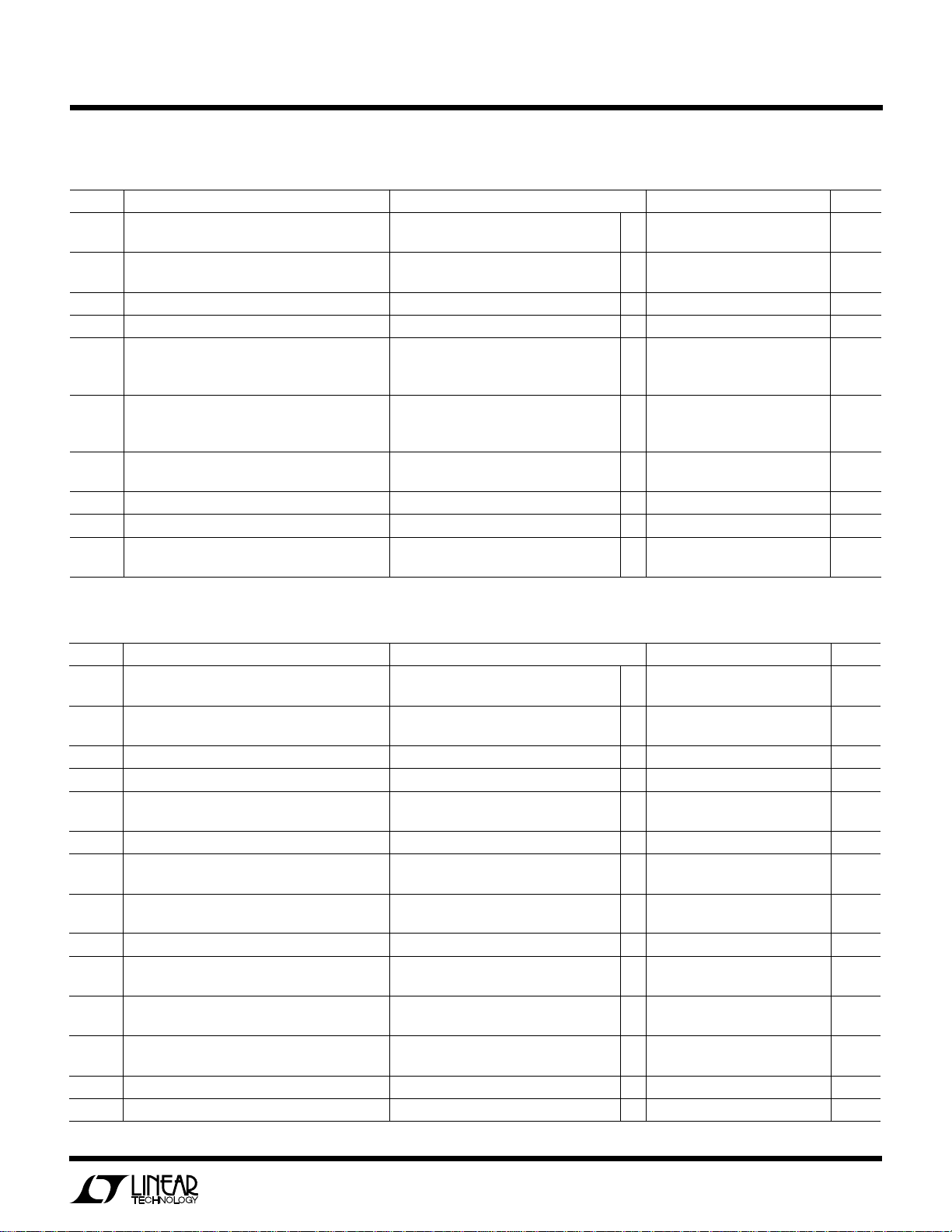
ELECTRICAL CHARACTERISTICS
TA = 25°C, VS = 5V,0V; VS = 3V,0V; VCM = V
SYMBOL PARAMETER CONDITIONS MIN TYP MAX UNITS
V
OS
∆V
I
B
∆I
B
I
OS
∆IOSInput Offset Current Shift VCM = V– to V
e
n
i
n
C
IN
A
VOL
Input Offset Voltage VCM = V
Input Offset Voltage Shift VCM = V– to V
OS
Input Offset Voltage Match (Channel-to-Channel) VCM = V+, V
Input Bias Current VCM = V
Input Bias Current Shift VCM = V– to V
Input Bias Current Match (Channel-to-Channel) VCM = V+ (Note 4) 0 10 100 nA
Input Offset Current VCM = V
Input Noise Voltage 0.1Hz to 10Hz 400 nV
Input Noise Voltage Density f = 1kHz 12 nV/√Hz
Input Noise Current Density f = 1kHz 0.3 pA/√Hz
Input Capacitance 5pF
Large-Signal Voltage Gain VS = 5V, VO = 75mV to 4.8V, RL = 10k 600 3800 V/mV
= half supply, unless otherwise noted.
OUT
+
–
= V
V
CM
= V
V
CM
= V– (Note 4) – 100 –10 0 nA
V
CM
= V
V
CM
= 3V, VO = 75mV to 2.8V, RL = 10k 500 2000 V/mV
V
S
+
–
(Note 4) 200 750 µV
+
–
+
+
–
+
150 475 µV
150 475 µV
150 425 µV
0 250 500 nA
–500 –250 0 nA
500 1000 nA
550 nA
550 nA
10 100 nA
P-P
2
Page 3
LT1498/LT1499
ELECTRICAL CHARACTERISTICS
TA = 25°C, VS = 5V,0V; VS = 3V,0V; VCM = V
SYMBOL PARAMETER CONDITIONS MIN TYP MAX UNITS
CMRR Common Mode Rejection Ratio VS = 5V, VCM = V– to V
CMRR Match (Channel-to-Channel) (Note 4) VS = 5V, VCM = V– to V
PSRR Power Supply Rejection Ratio VS = 2.2V to 12V, VCM = VO = 0.5V 88 105 dB
PSRR Match (Channel-to-Channel) (Note 4) VS = 2.2V to 12V, VCM = VO = 0.5V 82 103 dB
V
OL
V
OH
I
SC
I
S
GBW Gain-Bandwidth Product (Note 6) 6.8 10.5 MHz
SR Slew Rate (Note 7) VS = 5V, AV = –1, RL = Open, VO = 4V 2.6 4.5 V/µs
Output Voltage Swing (Low) (Note 5) No Load 14 30 mV
Output Voltage Swing (High) (Note 5) No Load 2.5 10 mV
Short-Circuit Current VS = 5V ±12.5 ±24 mA
Supply Current per Amplifier 1.7 2.2 mA
= half supply, unless otherwise noted.
OUT
+
= 3V, VCM = V– to V
V
S
= 3V, VCM = V– to V
V
S
= 0.5mA 35 70 mV
I
SINK
= 2.5mA 90 200 mV
I
SINK
I
= 0.5mA 50 100 mV
SOURCE
= 2.5mA 140 250 mV
I
SOURCE
= 3V ±12.0 ±19 mA
V
S
= 3V, AV = –1, RL = Open 2.3 4.0 V/µs
V
S
+
+
+
81 90 dB
76 86 dB
75 91 dB
70 86 dB
0°C < TA < 70°C, VS = 5V, 0V; VS = 3V, 0V; VCM = V
= half supply, unless otherwise noted.
OUT
SYMBOL PARAMETER CONDITIONS MIN TYP MAX UNITS
= V
V
CM
VCM = V
+
–
+ 0.1V ● 175 650 µV
+
+
–
+ 0.1V, V+ (Note 4) ● 200 900 µV
+
● 175 650 µV
● 1.5 4.0 µV/°C
● 170 600 µV
● 0 275 600 nA
V
OS
Input Offset Voltage VCM = V
VOS TC Input Offset Voltage Drift (Note 2) ● 0.5 2.5 µV/°C
∆V
OS
Input Offset Voltage Shift VCM = V– + 0.1V to V
Input Offset Voltage Match (Channel-to-Channel) VCM = V
I
B
Input Bias Current VCM = V
VCM = V– + 0.1V ● –600 –275 0 nA
∆I
B
Input Bias Current Shift VCM = V
Input Bias Current Match (Channel-to-Channel) VCM = V+ (Note 4) ● 0 15 170 nA
I
OS
∆I
OS
A
VOL
Input Offset Current VCM = V
Input Offset Current Shift VCM = V
Large-Signal Voltage Gain VS = 5V, VO = 75mV to 4.8V, RL = 10k ● 500 2500 V/mV
–
+ 0.1V to V
–
VCM = V
V
V
+ 0.1V (Note 4) ● –170 – 15 0 nA
+
–
= V
+ 0.1V ● 10 85 nA
CM
–
+ 0.1V to V
= 3V, VO = 75mV to 2.8V, RL = 10k ● 400 2000 V/mV
S
CMRR Common Mode Rejection Ratio VS = 5V, VCM = V– + 0.1V to V
= 3V, VCM = V– + 0.1V to V
V
S
CMRR Match (Channel-to-Channel) (Note 4) VS = 5V, VCM = V
= 3V, VCM = V
V
S
+
+
–
+ 0.1V to V
–
+ 0.1V to V
● 550 1200 nA
● 10 85 nA
● 20 170 nA
+
+
+
+
● 78 89 dB
● 73 85 dB
● 74 90 dB
● 69 86 dB
PSRR Power Supply Rejection Ratio VS = 2.3V to 12V, VCM = VO = 0.5V ● 86 102 dB
PSRR Match (Channel-to-Channel) (Note 4) VS = 2.3V to 12V, VCM = VO = 0.5V ● 80 102 dB
3
Page 4

LT1498/LT1499
ELECTRICAL CHARACTERISTICS
0°C < TA < 70°C, VS = 5V, 0V; VS = 3V, 0V; VCM = V
= half supply, unless otherwise noted.
OUT
SYMBOL PARAMETER CONDITIONS MIN TYP MAX UNITS
V
OL
V
OH
I
SC
I
S
Output Voltage Swing (Low) (Note 5) No Load ● 17 35 mV
= 0.5mA ● 40 80 mV
I
SINK
= 2.5mA ● 110 220 mV
I
SINK
Output Voltage Swing (High) (Note 5) No Load ● 3.5 15 mV
= 0.5mA ● 55 120 mV
I
SOURCE
= 2.5mA ● 160 300 mV
I
SOURCE
Short-Circuit Current VS = 5V ● ±12 ±23 mA
= 3V ● ±10 ±20 mA
V
S
Supply Current per Amplifier ● 1.9 2.6 mA
GBW Gain-Bandwidth Product (Note 6) ● 6.1 9 MHz
SR Slew Rate (Note 7) VS = 5V, AV = –1, RL = Open, VO = 4V ● 2.5 4.0 V/µs
= 3V, AV = –1, RL = Open ● 2.2 3.5 V/µs
V
S
–40°C < TA < 85°C, VS = 5V, 0V; VS = 3V, 0V; VCM = V
= half supply, unless otherwise noted. (Note 3)
OUT
SYMBOL PARAMETER CONDITIONS MIN TYP MAX UNITS
V
OS
Input Offset Voltage VCM = V
VOS TC Input Offset Voltage Drift (Note 2) ● 0.5 2.5 µV/°C
∆V
Input Offset Voltage Shift VCM = V– + 0.1V to V
OS
Input Offset Voltage Match (Channel-to-Channel) VCM = V
I
B
∆I
B
Input Bias Current VCM = V
Input Bias Current Shift VCM = V
Input Bias Current Match (Channel-to-Channel) VCM = V
I
OS
∆I
OS
A
VOL
Input Offset Current VCM = V
Input Offset Current Shift VCM = V– + 0.1V to V
Large-Signal Voltage Gain VS = 5V, VO = 75mV to 4.8V, RL = 10k ● 400 2500 V/mV
CMRR Common Mode Rejection Ratio VS = 5V, VCM = V– + 0.1V to V
CMRR Match (Channel-to-Channel) (Note 4) VS = 5V, VCM = V
+
–
= V
V
VCM = V
VCM = V
V
V
V
V
V
+ 0.1V ● 250 750 µV
CM
+
+
–
+ 0.1V, V
+
–
+ 0.1V ● –750 –350 0 nA
–
+ 0.1V to V
+
(Note 4) ● 0 30 180 nA
–
= V
CM
+
–
= V
CM
= 3V, VO = 75mV to 2.8V, RL = 10k ● 300 2000 V/mV
S
= 3V, VCM = V– + 0.1V to V
S
= 3V, VCM = V– + 0.1V to V
S
+
(Note 4) ● 300 1500 µV
+
+ 0.1V (Note 4) ● – 180 – 30 0 nA
+ 0.1V ● 15 90 nA
+
+
+
–
+ 0.1V to V
+
+
● 250 750 µV
● 1.5 4.0 µV/°C
● 250 650 µV
● 0 350 750 nA
● 700 1500 nA
● 15 90 nA
● 30 180 nA
● 77 86 dB
● 73 81 dB
● 72 86 dB
● 69 83 dB
PSRR Power Supply Rejection Ratio VS = 2.5V to 12V, VCM = VO = 0.5V ● 86 100 dB
PSRR Match (Channel-to-Channel) (Note 4) VS = 2.5V to 12V, VCM = VO = 0.5V ● 80 100 dB
V
OL
V
OH
Output Voltage Swing (Low) (Note 5) No Load ● 18 40 mV
= 0.5mA ● 45 80 mV
I
SINK
= 2.5mA ● 110 220 mV
I
SINK
Output Voltage Swing (High) (Note 5) No Load ● 3.5 15 mV
= 0.5mA ● 60 120 mV
I
SOURCE
I
= 2.5mA ● 170 300 mV
SOURCE
4
Page 5

ELECTRICAL CHARACTERISTICS
LT1498/LT1499
–40°C < TA < 85°C, VS = 5V, 0V; VS = 3V, 0V; VCM = V
= half supply, unless otherwise noted. (Note 3)
OUT
SYMBOL PARAMETER CONDITIONS MIN TYP MAX UNITS
I
SC
I
S
Short-Circuit Current VS = 5V ● ±7.5 ±15 mA
= 3V ● ±7.5 ±15 mA
V
S
Supply Current per Amplifier ● 2.0 2.7 mA
GBW Gain-Bandwidth Product (Note 6) ● 5.8 8.5 MHz
SR Slew Rate (Note 7) VS = 5V, AV = –1, RL = Open, VO = 4V ● 2.2 3.6 V/µs
= 3V, AV = –1, RL = Open ● 1.9 3.2 V/µs
V
S
TA = 25°C, VS = ±15V, VCM = 0V, V
= 0V, unless otherwise noted.
OUT
SYMBOL PARAMETER CONDITIONS MIN TYP MAX UNITS
V
∆V
OS
Input Offset Voltage VCM = V
Input Offset Voltage Shift VCM = V– to V
OS
Input Offset Voltage Match (Channel-to-Channel) VCM = V+, V
I
B
∆I
B
Input Bias Current VCM = V
Input Bias Current Shift VCM = V– to V
Input Bias Current Match (Channel-to-Channel) VCM = V
I
OS
Input Offset Current VCM = V
∆IOSInput Offset Current Shift VCM = V– to V
Input Noise Voltage 0.1Hz to 10Hz 400 nV
e
n
i
n
A
VOL
Input Noise Voltage Density f = 1kHz 12 nV/√Hz
Input Noise Current Density f = 1kHz 0.3 pA/√Hz
Large-Signal Voltage Gain VO = –14.5V to 14.5V, RL = 10k 1000 5200 V/mV
+
–
= V
V
CM
= V
V
CM
= V– (Note 4) –120 –12 0 nA
V
CM
= V
V
CM
= –10V to 10V, RL = 2k 500 2300 V/mV
V
O
+
–
(Note 4) 250 1400 µV
+
–
+
+
(Note 4) 0 12 120 nA
+
–
+
0 250 550 nA
–550 –250 0 nA
200 800 µV
200 800 µV
150 650 µV
500 1100 nA
660 nA
660 nA
12 120 nA
P-P
Channel Separation VO = –10V to 10V, RL = 2k 116 130 dB
CMRR Common-Mode Rejection Ratio VCM = V– to V
CMRR Match (Channel-to-Channel) (Note 4) VCM = V– to V
+
+
93 106 dB
87 103 dB
PSRR Power Supply Rejection Ratio VS = ±5V to ±15V 89 110 dB
PSRR Match (Channel-to-Channel) (Note 4) VS = ±5V to ±15V 83 105 dB
V
OL
V
OH
I
SC
I
S
Output Voltage Swing (Low) (Note 5) No Load 18 30 mV
= 0.5mA 40 80 mV
I
SINK
I
= 10mA 230 500 mV
SINK
Output Voltage Swing (High) (Note 5) No Load 2.5 10 mV
I
= 0.5mA 55 120 mV
SINK
= 10mA 420 800 mV
I
SINK
Short-Circuit Current ±15 ±30 mA
Supply Current per Amplifier 1.8 2.5 mA
GBW Gain-Bandwidth Product (Note 6) 6.8 10.5 MHz
SR Slew Rate AV = –1, RL = Open, VO = ±10V 3.5 6 V/µs
Measure at V
= ±5V
O
5
Page 6

LT1498/LT1499
ELECTRICAL CHARACTERISTICS
0°C < TA < 70°C, VS = ±15V, VCM = 0V, V
SYMBOL PARAMETER CONDITIONS MIN TYP MAX UNITS
V
OS
VOS TC Input Offset Voltage Drift (Note 2) ● 1.0 3.5 µV/°C
∆V
I
B
∆I
B
I
OS
∆I
OS
A
VOL
CMRR Common Mode Rejection Ratio VCM = V– + 0.1V to V
PSRR Power Supply Rejection Ratio VS = ±5V to ±15V ● 88 103 dB
V
OL
V
OH
I
SC
I
S
GBW Gain-Bandwidth Product (Note 6) ● 6.1 9 MHz
SR Slew Rate AV = –1, RL = Open, VO = ±10V ● 3.4 5.3 V/µs
Input Offset Voltage VCM = V
Input Offset Voltage Shift VCM = V– + 0.1V to V
OS
Input Offset Voltage Match (Channel-to-Channel) VCM = V
Input Bias Current VCM = V
Input Bias Current Shift VCM = V
Input Bias Current Match (Channel-to-Channel) VCM = V
Input Offset Current VCM = V
Input Offset Current Shift VCM = V– + 0.1V to V
Large-Signal Voltage Gain VO = –14.5V to 14.5V, RL = 10k ● 900 5000 V/mV
Channel Separation VO = –10V to 10V, RL = 2k ● 112 125 dB
CMRR Match (Channel-to-Channel) (Note 4) VCM = V
PSRR Match (Channel-to-Channel) (Note 4) VS = ±5V to ±15V ● 82 103 dB
Output Voltage Swing (Low) (Note 5) No Load ● 18 40 mV
Output Voltage Swing (High) (Note 5) No Load ● 3.5 15 mV
Short-Circuit Current ● ±12 ±28 mA
Supply Current per Amplifier ● 1.9 2.8 mA
= 0V, unless otherwise noted.
OUT
+
–
= V
V
V
V
V
V
V
I
SINK
I
SINK
I
SOURCE
I
SOURCE
Measured at V
+ 0.1V ● 200 900 µV
CM
+
= V
CM
–
+ 0.1V, V
+
–
= V
+ 0.1V ● –675 –300 0 nA
CM
–
+ 0.1V to V
+
(Note 4) ● 0 20 180 nA
–
= V
CM
CM
O
+ 0.1V (Note 4) ● – 180 – 20 0 nA
+
–
= V
+ 0.1V ● 15 90 nA
= –10V to 10V, RL = 2k ● 400 2000 V/mV
–
+ 0.1V to V
= 0.5mA ● 45 90 mV
= 10mA ● 270 520 mV
= 0.5mA ● 60 120 mV
= 10mA ● 480 1000 mV
= ±5V
O
● 200 900 µV
● 2.0 5.0 µV/°C
+
+
(Note 4) ● 350 1500 µV
+
+
+
+
● 200 750 µV
● 0 300 675 nA
● 600 1350 nA
● 15 90 nA
● 30 180 nA
● 92 103 dB
● 86 103 dB
6
Page 7

LT1498/LT1499
ELECTRICAL CHARACTERISTICS
–40°C < TA < 85°C, VS = ±15V, VCM = 0V, V
SYMBOL PARAMETER CONDITIONS MIN TYP MAX UNITS
V
OS
VOS TC Input Offset Voltage Drift (Note 2) ● 1.0 3.5 µV/°C
∆V
I
B
∆I
B
I
OS
∆I
OS
A
VOL
CMRR Common Mode Rejection Ratio VCM = V– + 0.1V to V
PSRR Power Supply Rejection Ratio VS = ±5V to ±15V ● 88 100 dB
V
OL
V
OH
I
SC
I
S
GBW Gain-Bandwidth Product (Note 6) ● 5.8 8.5 MHz
SR Slew Rate AV = –1, RL = Open, VO = ±10V, ● 3 4.75 V/µs
Input Offset Voltage VCM = V
Input Offset Voltage Shift VCM = V– + 0.1V to V
OS
Input Offset Voltage Match (Channel-to-Channel) VCM = V
Input Bias Current VCM = V
Input Bias Current Shift VCM = V
Input Bias Current Match (Channel-to-Channel) VCM = V
Input Offset Current VCM = V
Input Offset Current Shift VCM = V– + 0.1V to V
Large-Signal Voltage Gain VO = –14.5V to 14.5V, RL = 10k ● 800 5000 V/mV
Channel Separation VO = –10V to 10V, RL = 2k ● 110 120 dB
CMRR Match (Channel-to-Channel) (Note 4) VCM = V
PSRR Match (Channel-to-Channel) (Note 4) VS = ±5V to ±15V ● 82 100 dB
Output Voltage Swing (Low) (Note 5) No Load ● 25 50 mV
Output Voltage Swing (High) (Note 5) No Load ● 3.5 15 mV
Short-Circuit Current ● ±10 ±18 mA
Supply Current per Amplifier ● 2.0 3.0 mA
= 0V, unless otherwise noted. (Note 3)
OUT
+
–
= V
V
V
V
V
V
V
I
SINK
I
SINK
I
SOURCE
I
SOURCE
Measure at V
+ 0.1V ● 300 950 µV
CM
+
= V
CM
–
+ 0.1V, V
+
–
= V
+ 0.1V ● – 800 – 350 0 nA
CM
–
+ 0.1V to V
+
(Note 4) ● 0 20 200 nA
–
= V
CM
CM
O
+ 0.1V (Note 4) ● –200 –20 0 nA
+
–
= V
+ 0.1V ● 15 100 nA
= –10V to 10V, RL = 2k ● 350 2000 V/mV
–
+ 0.1V to V
+
+
(Note 4) ● 350 1800 µV
+
+
+
+
= 0.5mA ● 50 100 mV
= 10mA ● 275 520 mV
= 0.5mA ● 65 120 mV
= 10mA ● 500 1000 mV
= ±5V
O
● 300 950 µV
● 2.0 5.0 µV/°C
● 250 850 µV
● 0 350 800 nA
● 700 1600 nA
● 15 100 nA
● 30 200 nA
● 90 101 dB
● 86 100 dB
● denotes specifications that apply over the full operating temperature
The
range.
Note 1: A heat sink may be required to keep the junction temperature
below the absolute maximum rating when the output is shorted
indefinitely.
Note 2: This parameter is not 100% tested.
Note 3: The LT1498/LT1499 are designed, characterized and expected to
meet these extended temperature limits, but are not tested at –40°C and
85°C. Guaranteed I grade parts are available, consult factory.
Note 4: Matching parameters are the difference between amplifiers A and
D and between B and C on the LT1499; between the two amplifiers on the
LT1498.
Note 5: Output voltage swings are measured between the output and
power supply rails.
Note 6: V
= 3V, VS = ±15V GBW limit guaranteed by correlation to
S
5V tests.
Note 7: V
= 3V, VS = 5V slew rate limit guaranteed by correlation to
S
±15V tests.
7
Page 8

LT1498/LT1499
INPUT OFFSET VOLTAGE (µV)
–500
PERCENT OF UNITS (%)
15
20
25
300
1498/99 G02
10
5
0
–300
–100
100
500
LT1498: N8, S8 PACKAGES
LT1499: S14 PACKAGE
V
S
= 5V, 0V
V
CM
= 0V TO 5V
COMMON MODE VOLTAGE (V)
–2
INPUT BIAS CURRENT (nA)
0
200
23456
1498/99 G06
–200
–400
–1
0
1
400
–100
100
–300
300
VS = 5V, 0V
T
A
= 125°C
TA = 25°C TA = –55°C
LOAD CURRENT (mA)
10
SATURATION VOLTAGE (mV)
100
0.001 0.1 1 10
1498/99 G09
1
0.01
1000
TA = –55°C
TA = 25°C
T
A
= 125°C
W
U
TYPICAL PERFORMANCE CHARACTERISTICS
VOS Distribution, VCM = 0V
(PNP Stage)
25
LT1498: N8, S8 PACKAGES
LT1499: S14 PACKAGE
= 5V, 0V
V
S
20
= 0V
V
CM
15
10
PERCENT OF UNITS (%)
5
0
–500
–300
INPUT OFFSET VOLTAGE (µV)
–100
100
Supply Current vs Supply Voltage
2.0
1.5
1.0
TA = 125°C
TA = 25°C
TA = –55°C
300
1498/99 G01
500
VOS Distribution VCM = 5V
(NPN Stage)
25
LT1498: N8, S8 PACKAGES
LT1499: S14 PACKAGE
= 5V, 0V
V
S
20
= 5V
V
CM
15
10
PERCENT OF UNITS (%)
5
0
–300
–500
2.0
1.5
1.0
–100
INPUT OFFSET VOLTAGE (µV)
VS = ±15V
100
VS = 5V, 0V
300
∆VOS Shift for VCM = 0V to 5V
500
1498/99 G02
Input Bias Current
vs Common Mode VoltageSupply Current vs Temperature
0.5
SUPPLY CURRENT PER AMPLIFIER (mA)
0
436
0
16
8
12
TOTAL SUPPLY VOLTAGE (V)
Input Bias Current vs Temperature
400
300
200
100
0
–100
–200
INPUT BIAS CURRENT (nA)
–300
–400
8
–35 85
–50
NPN ACTIVE
PNP ACTIVE
–20
–5
10
TEMPERATURE (°C)
20
40
25
24
55
32
28
1498/99 G04
VS = ±15V
= 15V
V
CM
VS = 5V, 0V
= 5V
V
CM
VS = ±15V
= –15V
V
CM
VS = 5V, 0V
= 0V
V
CM
70
1498/99 G07
100
0.5
SUPPLY CURRENT PER AMPLIFIER (mA)
0
–25 0 50
–50
25
TEMPERATURE (°C)
75 100 125
Output Saturation Voltage
vs Load Current (Output High)
1000
100
10
TA = –55°C
SATURATION VOLTAGE (mV)
1
0.001 0.1 1 10
TA = 125°C
TA = 25°C
0.01
LOAD CURRENT (mA)
1498/99 G05
Output Saturation Voltage
vs Load Current (Output Low)
1498/99 G08
Page 9

W
FREQUENCY (Hz)
1
80
NOISE VOLTAGE (nV/√Hz)
100
120
140
160
10 100 1000
1498/99 G12
60
40
20
0
180
200
VS = 5V, 0V
VCM = 2.5V
PNP ACTIVE
VCM = 4V
NPN ACTIVE
FREQUENCY (kHz)
40
COMMON MODE REJECTION RATIO (dB)
60
80
70
100
120
30
50
90
110
1 100 1000 10000
1498/99 G15
20
10
VS = ±15V
V
S
= ±2.5V
FREQUENCY (kHz)
0.01
–110
CHANNEL SEPARATION (dB)
–100
–90
–80
–70
0.1 1 10 100 1000
1498/99 G18
–120
–130
–140
–150
–60
–50
VS = ±15V
V
OUT
= ±1V
P-P
R
L
= 2k
U
TYPICAL PERFORMANCE CHARACTERISTICS
0.1Hz to 10Hz
Minimum Supply Voltage
300
250
200
150
Output Voltage Noise
VS = ±2.5V
= 0V
V
CM
LT1498/LT1499
Noise Voltage Spectrum
100
50
CHANGE IN OFFSET VOLTAGE (µV)
0
1
TA = 85°C
T
= 25°C
A
23
TOTAL SUPPLY VOLTAGE (V)
Noise Current Spectrum
10
VS = 5V, 0V
9
8
7
6
5
CURRENT NOISE (pA/√Hz)
4
3
2
1
0
1
VCM = 4V
NPN ACTIVE
VCM = 2.5V
PNP ACTIVE
10 100 1000
FREQUENCY (Hz)
PSRR vs Frequency
90
80
70
60
50
NEGATIVE SUPPLY
40
30
20
10
0
POWER SUPPLY REJECTION RATIO (dB)
–10
1 100 1000 10000
10
FREQUENCY (kHz)
TA = 70°C
NONFUNCTIONAL
= –55°C
T
A
4
VS = ±2.5V
POSITIVE SUPPLY
1498/99 G10
1498/99 G13
1498/99 G16
OUTPUT VOLTAGE (200nV/DIV)
5
010
Gain and Phase vs Frequency
70
60
50
40
30
20
10
VOLTAGE GAIN (dB)
0
–10
–20
–30
0.01 1 10 100
Gain Bandwidth and Phase
Margin vs Supply Voltage
20
18
16
14
12
10
8
6
GAIN BANDWIDTH (MHz)
4
2
0
0
TIME (1s/DIV)
GAIN
0.1
FREQUENCY (MHz)
PHASE MARGIN
GAIN BANDWIDTH
5
TOTAL SUPPLY VOLTAGE (V)
15 20
10
1498/99 G11
RL = 10k
V
= ±1.5V
S
= ±15V
V
S
PHASE
1498/99 G14
25
1498/99 G17
180
144
108
PHASE SHIFT (DEG)
72
36
0
–36
–72
–108
–144
–180
100
90
80
PHASE MARGIN (DEG)
70
60
50
40
30
20
10
0
30
CMRR vs Frequency
Channel Separation vs Frequency
9
Page 10

LT1498/LT1499
FREQUENCY (kHz)
0.01
THD + NOISE (%)
0.01
0.1
1
0.1 1 10 100
1498/99 G26
0.001
VS = ±1.5V
V
IN
= 2V
P-P
R
L
= 10k
AV = 1
AV = –1
W
U
TYPICAL PERFORMANCE CHARACTERISTICS
Capacitive Load Handling
70
VS = 5V, 0V
= 1
A
V
60
= 1k
R
L
50
40
30
OVERSHOOT (%)
20
10
0
10 1000 10000 100000
100
CAPACITIVE LOAD (pF)
1498/99 G19
Slew Rate vs Supply Voltage
9
V
= 80% OF VS
OUT
= –1
A
V
8
7
6
5
SLEW RATE (V/µs)
4
3
412
8
0
TOTAL SUPPLY VOLTAGE (V)
RISING EDGE
FALLING EDGE
20 36
16
28
24
32
1498/99 G20
Output Step vs
Settling Time to 0.01%
10
VS = ±15V
8
NONINVERTING
6
4
2
0
–2
OUTPUT STEP (V)
–4
–6
NONINVERTING
–8
–10
1.5
2.0
SETTLING TIME (µs)
INVERTING
2.5
INVERTING
3.0
3.5
1498/99 G21
Open-Loop Gain
20
15
10
5
0
–5
INPUT VOLTAGE (µV)
–10
–15
–20
–20 –15
R
R
= 10k
L
–10 –5
L
OUTPUT VOLTAGE (V)
1
0.1
0.01
THD + NOISE (%)
0.001
0.0001
0234
Open-Loop Gain
INPUT VOLTAGE (µV)
4
3
2
1
0
–1
–2
–3
–4
V
0
= 5V, 0V
S
R
L
R
L
= 2k
05
VS = ±15V
10 15
1498/99 G22
20
Total Harmonic Distortion + Noise
vs Peak-to-Peak Voltage
f = 1kHz
= 10k
R
L
AV = 1
= ±1.5V
V
S
A
= –1
V
= ±1.5V
V
S
1
INPUT VOLTAGE (V
AV = 1
= ±2.5V
V
S
AV = –1
= ±2.5V
V
S
)
P-P
1498/99 G25
= 2k
= 10k
12 4
5
3
OUTPUT VOLTAGE (V)
Warm-Up Drift vs Time
10
S8 PACKAGE, VS = ±2.5V
N8 PACKAGE, VS = ±2.5V
LT1499CS, V
S8 PACKAGE, VS = ±15V
20 40
60 100 160
TIME AFTER POWER-UP (SEC)
5
1498/99 G23
6
CHANGE IN OFFSET VOLTAGE (µV)
–10
–20
–30
–40
0
0
Total Harmonic Distortion + Noise
vs Frequency
= ±2.5V
S
N8 PACKAGE, VS = ±15V
LT1499CS, VS = ±15V
80
120 140
1498/99 G24
10
Page 11

W
U
TYPICAL PERFORMANCE CHARACTERISTICS
LT1498/LT1499
5V Small-Signal Response
5mV/DIV
= 1
A
V
V
IN
R
= 1k
L
= 20mV
P-P
200ns/DIVVS = 5V
AT 50kHz
±15V Small-Signal Response
5mV/DIV
1498/99 G27
5V Large-Signal Response
1V/DIV
V
= 5V
S
A
= 1
V
V
= 4V
AT 10kHz
IN
P-P
= 1k
R
L
2µs/DIV
±15V Large-Signal Response
5V/DIV
1498/99 G28
VS = ±15V
= 1
A
V
V
= 20mV
IN
R
= 1k
L
AT 50kHz
P-P
200ns/DIV
U
1498/99 G29
WUU
APPLICATIONS INFORMATION
Rail-to-Rail Input and Output
The LT1498/LT1499 are fully functional for an input and
output signal range from the negative supply to the positive supply. Figure 1 shows a simplified schematic of the
amplifier. The input stage consists of two differential
amplifiers, a PNP stage (Q1/Q2) and an NPN stage (Q3/
Q4) which are active over different ranges of input common mode voltage. A complementary common emitter
output stage (Q14/Q15) is employed allowing the output
to swing from rail-to-rail. The devices are fabricated on
Linear Technology’s proprietary complementary bipolar
process to ensure very similar DC and AC characteristics
for the output devices (Q14/Q15).
1498/99 G30
A
V
R
= 1
V
= 20V
IN
= 1k
L
P-P
2µs/DIVVS = ±15V
AT 10kHz
The PNP differential input pair is active for input common
mode voltages, VCM, between the negative supply to
approximately 1.3V below the positive supply. As V
CM
moves further toward the positive supply, the transistor
Q5 will steer the tail current, I1, to the current mirror Q6/
Q7 activating the NPN differential pair, and the PNP
differential pair becomes inactive for the rest of the input
common mode range up to the positive supply.
The output is configured with a pair of complementary
common emitter stages that enables the output to swing
from rail to rail. Capacitors C1 and C2 form local feedback
loops that lower the output impedance at high frequencies.
11
Page 12

LT1498/LT1499
U
WUU
APPLICATIONS INFORMATION
+
V
D1
+IN
–IN
V
R6
D6D5
R7
–
D2
Q4
Q3
Q7
Figure 1. LT1498 Simplified Schematic Diagram
V
Q5
Q6
BIAS
R3
R4 R5
I
1
Q1
Q2
D3
D4
Q10
Q12
Q11 Q13
V
Q9
Q8
R1
R2
–
OUTPUT BIAS
C
C
BUFFER
AND
Q15
C2
OUT
C1
Q14
1498/99 F01
Input Offset Voltage
The offset voltage changes depending upon which input
stage is active. The input offsets are random, but are
trimmed to less than 475µV. To maintain the precision
characteristics of the amplifier, the change of VOS over the
entire input common mode range (CMRR) is guaranteed
to be less than 425µV on a single 5V supply.
Input Bias Current
The input bias current polarity also depends on the input
common mode voltage, as described in the previous
section. When the PNP differential pair is active, the input
bias currents flow out of the input pins; they flow in
opposite direction when the NPN input stage is active. The
offset error due to input bias current can be minimized by
equalizing the noninverting and inverting input source
impedances. This will reduce the error since the input
offset currents are much less than the input bias currents.
Overdrive Protection
To prevent the output from reversing polarity when the
input voltage exceeds the power supplies, two pair of
crossing diodes D1 to D4 are employed. When the input
voltage exceeds either power supply by approximately
700mV, D1/D2 or D3/D4 will turn on, forcing the output to
the proper polarity. For the phase reversal protection to
work properly, the input current must be less than 5mA.
If
the amplifier is to be severely overdriven, an external
resistor should be used to limit the overdrive current.
Furthermore, the LT1498/LT1499’s input stages are protected by a pair of back-to-back diodes, D5/D6. When a
differential voltage of more than 0.7V is applied to the
inputs, these diodes will turn on, preventing the Zener
breakdown of the input transistors. The current in D5/D6
should be limited to less than 10mA. Internal resistors R6
and R7 (700Ω total) limit the input current for differential
input signals of 7V or less. For larger input levels, a
resistor in series with either or both inputs should be
used to limit the current. Worst-case differential input
voltage usually occurs when the output is shorted to
ground. In addition, the amplifier is protected against
ESD strikes up to 3kV on all pins.
Capacitive Load
The LT1498/LT1499 are designed for ease of use. The
amplifier can drive a capacitive load of more than 10nF
12
Page 13

LT1498/LT1499
U
WUU
APPLICATIONS INFORMATION
without oscillation at unity gain. When driving a heavy
capacitive load, the bandwidth is reduced to maintain
stability. Figures 2a and 2b illustrate the stability of the
device for small-signal and large-signal conditions with
capacitive loads. Both the small-signal and large-signal
transient response with a 10nF capacitive load are well
behaved.
Feedback Components
To minimize the loading effect of feedback, it is possible to
use the high value feedback resistors to set the gain.
However, care must be taken to insure that the pole formed
by the feedback resistors and the total input capacitance at
the inverting input does not degrade the stability of the
amplifier. For instance, the LT1498/LT1499 in a noninverting gain of 2, set with two 30k resistors, will probably
oscillate with 10pF total input capacitance (5pF input
capacitance + 5pF board capacitance). The amplifier has a
2.5MHz crossing frequency and a 60° phase margin at 6dB
of gain. The feedback resistors and the total input capacitance create a pole at 1.06MHz that induces 67° of phase
shift at 2.5MHz! The solution is simple, either lower the
value of the resistors or add a feedback capacitor of 10pF
of more.
= 0pF
C
L
C
= 500pF
L
CL = 10nF
= 0pF
C
L
C
= 500pF
L
CL = 10nF
VS = 5V
A
= 1
V
1498/99 F02a
Figure 2a. LT1498 Small-Signal Response
VS = 5V
= 1
A
V
1498/99 F02b
Figure 2b. LT1498 Large-Signal Response
U
TYPICAL APPLICATIONS N
1A Voltage Controlled Current Source 1A Voltage Controlled Current Sink
500pF
0.5Ω
0.5Ω
1k
100Ω
I
OUT
+
V
–
1/2 LT1498
1k
V
IN
+
V+ – VIN
I
=
OUT
< 1µs
t
r
Si9430DY
R
L
1498/99 TA03
+
I
OUT
V
R
L
Si9410DY
0.5Ω
1498/99 TA04
+
V
1k
V
IN
+
1/2 LT1498
–
I
=
OUT
tr < 1µs
V
0.5Ω
IN
100Ω
500pF
1k
13
Page 14

LT1498/LT1499
U
TYPICAL APPLICATIONS N
Input Bias Current Cancellation
PACKAGE DESCRIPTION
–
1/2 LT1498
+
R
F
SIGNAL
AMP
V
OUT
R
G
V
IN
1M
+
1/2 LT1498
22pF
1M
INPUT BIAS CURRENT LESS THAN 50nA
FOR 500mV ≤ V
≤ (V+ – 500mV)
IN
CANCELLATION
AMP
–
1498/99 TA05
U
Dimensions in inches (millimeters) unless otherwise noted.
N8 Package
8-Lead PDIP (Narrow 0.300)
(LTC DWG # 05-08-1510)
876
0.255 ± 0.015*
(6.477 ± 0.381)
0.300 – 0.325
(7.620 – 8.255)
0.065
(1.651)
0.009 – 0.015
(0.229 – 0.381)
+0.025
0.325
–0.015
+0.635
8.255
()
–0.381
*THESE DIMENSIONS DO NOT INCLUDE MOLD FLASH OR PROTRUSIONS.
MOLD FLASH OR PROTRUSIONS SHALL NOT EXCEED 0.010 INCH (0.254mm)
TYP
(2.540 ± 0.254)
12
0.045 – 0.065
(1.143 – 1.651)
0.005
(0.127)
MIN
0.100 ± 0.010
0.400*
(10.160)
MAX
3
5
4
0.130 ± 0.005
(3.302 ± 0.127)
0.125
(3.175)
MIN
0.018 ± 0.003
(0.457 ± 0.076)
0.015
(0.380)
MIN
N8 0695
14
Page 15

PACKAGE DESCRIPTION
U
Dimensions in inches (millimeters) unless otherwise noted.
S8 Package
8-Lead Plastic Small Outline (Narrow 0.150)
(LTC DWG # 05-08-1610)
0.189 – 0.197*
(4.801 – 5.004)
7
8
5
6
LT1498/LT1499
0.010 – 0.020
(0.254 – 0.508)
0.008 – 0.010
(0.203 – 0.254)
*
DIMENSION DOES NOT INCLUDE MOLD FLASH. MOLD FLASH
SHALL NOT EXCEED 0.006" (0.152mm) PER SIDE
**
DIMENSION DOES NOT INCLUDE INTERLEAD FLASH. INTERLEAD
FLASH SHALL NOT EXCEED 0.010" (0.254mm) PER SIDE
× 45°
0°– 8° TYP
0.016 – 0.050
0.406 – 1.270
14-Lead Plastic Small Outline (Narrow 0.150)
(LTC DWG # 05-08-1610)
0.228 – 0.244
(5.791 – 6.197)
S Package
14
0.053 – 0.069
(1.346 – 1.752)
0.014 – 0.019
(0.355 – 0.483)
13
1
0.337 – 0.344*
(8.560 – 8.738)
12
11 10
0.150 – 0.157**
(3.810 – 3.988)
3
2
4
0.004 – 0.010
(0.101 – 0.254)
0.050
(1.270)
TYP
8
9
SO8 0996
0.228 – 0.244
(5.791 – 6.197)
0.010 – 0.020
(0.254 – 0.508)
0.008 – 0.010
(0.203 – 0.254)
*
DIMENSION DOES NOT INCLUDE MOLD FLASH. MOLD FLASH
SHALL NOT EXCEED 0.006" (0.152mm) PER SIDE
**
DIMENSION DOES NOT INCLUDE INTERLEAD FLASH. INTERLEAD
FLASH SHALL NOT EXCEED 0.010" (0.254mm) PER SIDE
× 45°
0° – 8° TYP
0.016 – 0.050
0.406 – 1.270
Information furnished by Linear Technology Corporation is believed to be accurate and reliable.
However, no responsibility is assumed for its use. Linear Technology Corporation makes no representation that the interconnection of its circuits as described herein will not infringe on existing patent rights.
0.053 – 0.069
(1.346 – 1.752)
0.014 – 0.019
(0.355 – 0.483)
0.150 – 0.157**
(3.810 – 3.988)
1
3
2
4
5
0.050
(1.270)
TYP
7
6
0.004 – 0.010
(0.101 – 0.254)
S14 0695
15
Page 16

LT1498/LT1499
TYPICAL APPLICATION
Bidirectional Current Sensor
U
A bidirectional current sensor for battery-powered systems is shown in Figure 3. Two outputs are provided: one
proportional to charge current, the other proportional to
discharge current. The circuit takes advantage of the
LT1498’s rail-to-rail input range and its output phase
reversal protection. During the charge cycle, the op amp
A1 forces a voltage equal to (IL)(R
) across RA. This
SENSE
V
BATTERY
A2
1/2 LT1498
Figure 3. Bidirectional Current Sensor
CHARGE
DISCHARGE
+
–
I
L
R
A
R
A
Q2
MTP23P06
DISCHARGE
OUT
R
B
R
SENSE
0.1Ω
voltage is then amplified at the Charge Out by the ratio of
RB over RA. In this mode, the output of A2 remains high,
keeping Q2 off and the Discharge Out low, even though the
(+) input of A2 exceeds the positive power supply. During
the discharge cycle, A2 and Q2 are active and the operation
is similar to the charge cycle.
V
BATTERY
R
A
+
A1
R
MTP23P06
CHARGE
OUT
1/2 LT1498
A
–
Q1
R
B
= I
V
O
FOR R
R
B
V
O
I
L
R
L
SENSE
()
R
A
= 1k, RB = 10k
A
= 1V/A
1498/99 F03
RELATED PARTS
PART NUMBER DESCRIPTON COMMENTS
LTC®1152 Rail-to-Rail Input and Output, Zero-Drift Op Amp High DC Accuracy, 10µV V
1V/µs Slew Rate, Max Supply Current 2.2mA
LT1211/LT1212 Dual/Quad 14MHz, 7V/µs, Single Supply Precision Op Amps Input Common Mode Includes Ground, 275µV V
6µV/°C Max Drift, Max Supply Current 1.8mA per Op Amp
LT1213/LT1214 Dual/Quad 28MHz, 12V/µs, Single Supply Precision Op Amps Input Common Mode Includes Ground, 275µV V
6µV/°C Max Drift, Max Supply Current 3.5mA per Op Amp
LT1215/LT1216 Dual/Quad 23MHz, 50V/µs, Single Supply Precision Op Amps Input Common Mode Includes Ground, 450µV V
Max Supply Current 6.6mA per Op Amp
LT1366/LT1367 Dual/Quad Precision, Rail-to-Rail Input and Output Op Amps 475µV V
, 400kHz GBW, 0.13V/µs Slew Rate,
OS(MAX)
Max Supply Current 520µA per Op Amp
LT1490/LT1491 Dual/Quad Micropower, Rail-to-Rail Input and Output Op Amps Max Supply Current 50µA per Op Amp, 200kHz GBW, 0.07V/µs
Slew Rate, Operates with Inputs 44V Above V
+
of V
Linear Technology Corporation
16
1630 McCarthy Blvd., Milpitas, CA 95035-7417 ● (408) 432-1900
FAX: (408) 434-0507
●
TELEX: 499-3977 ● www.linear-tech.com
, 100nV/°C Drift, 1MHz GBW,
OS(MAX)
,
OS(MAX)
,
OS(MAX)
,
OS(MAX)
–
Independent
14989f LT/TP 0397 7K • PRINTED IN USA
LINEAR TECHNOLOGY CORPORATION 1996
 Loading...