

Page 1

FEATURES
■
Gain-Bandwidth Product: 5MHz Typ
■
Slew Rate: 3V/µs Typ
■
Low Supply Current per Amplifier: 0.55mA Max
■
Input Offset Voltage: 180µV Max
■
Input Offset Voltage Drift: 3µV/°C Max
■
Input Offset Current: 20nA Max
■
Input Bias Current: 100nA Max
■
Open-Loop Gain: 1500V/mV Min (VS = ±15V)
■
Low Input Noise Voltage: 16.5nV/√Hz
■
Low Input Noise Current: 0.14pA/√Hz
■
Large Output Drive Current: 20mA Min
■
Single Supply Operation
Input Voltage Range Includes Ground
Output Swings to Ground While Sinking Current
■
Wide Supply Voltage Range: 2.5V to 36V
■
Specified on 3.3V, 5V and ±15V
■
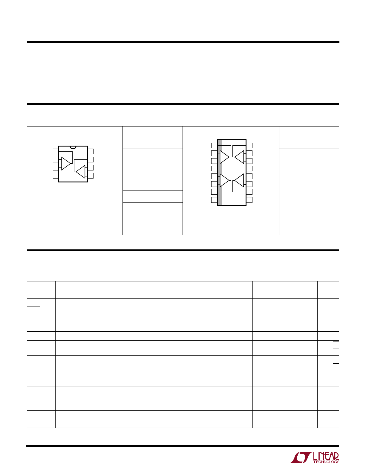
Dual in 8-Pin PDIP and SO Package
■
Quad in a Narrow 16-Pin SO Package
LT1492/LT1493
5MHz, 3V/µs, Low Power
Single Supply, Dual and Quad
Precision Op Amps
U
DESCRIPTION
The LT®1492/LT1493 are dual/quad, low power, single supply precision op amps with 5MHz gain-bandwidth product,
3V/µs slew rate and only 450µ A of quiescent supply current
per amplifier.
With a maximum input offset voltage of only 180µV, the
LT1492/LT1493 eliminate trims in most systems while providing high frequency performance not usually found in low
power single supply amplifiers.
The LT1492/LT1493 will operate on any supply greater than
2.5V and less than 36V total, and are specified on single 3.3V,
single 5V and ±15V supplies. Even with their low quiescent
supply current the minimum output drive is 20mA, ideal for
driving low impedance loads.
The inputs can be driven beyond the supplies without
damage or phase reversal of the output. The low operating
voltage and wide input and output range make the LT1492/
LT1493 amplifiers ideal for battery-powered applications.
U
APPLICATIONS
■
Battery-Powered Systems
Portable Instrumentation
■
Active Filters
■
Photodiode Amplifiers
■
DAC Current to Voltage Amplifiers
TYPICAL APPLICATION
Precision AC to DC Converter (Full Wave Rectifier and Filter)
4.99k
5V
10k
V
IN
–
1/2 LT1492
+
15k
U
+
1/2 LT1492
–
10k
6.49k
VS = 5V, 0V
< 1% ERROR FROM 100mV TO 1V, f = 1kHz
10% ERROR AT 10mV, f = 1kHz
1% ERROR AT 5kHz, V
10% ERROR AT 30kHz, V
10k
+
= 100mV
IN
For applications requiring faster precision single supply
amplifiers, see the 14MHz, 7V/µs LT1211/LT1212, the
28MHz, 12V/µs LT1213/LT1214 or the 23MHz, 50V/µs
LT1215/LT1216.
, LTC and LT are registered trademarks of Linear Technology Corporation.
Distribution of Offset Voltage
Drift with Temperature
50
VS = 5V, 0V
LT1492 N8, S8 PACKAGES
LT1493 S16 PACKAGE
40
30
DC
V
10µF
= 100mV
IN
OUT
RMS
RMS
1492/93 TA01
20
PERCENT OF UNITS (%)
10
0
–1.5
–1
–2 2
–2.5
OFFSET VOLTAGE DRIFT WITH TEMPERATURE (µV/°C)
–0.5
0.5
1
0
1.5
2.5
1492/93 G02
1
Page 2
LT1492/LT1493
1
2
3
4
5
6
7
8
TOP VIEW
S PACKAGE
16-LEAD PLASTIC SO
16
15
14
13
12
11
10
9
OUT A
–IN A
+IN A
V
+
+IN B
–IN B
OUT B
NC
OUT D
–IN D
+IN D
V
–
+IN C
–IN C
OUT C
NC
C
A
D
B
WW
W
U
ABSOLUTE MAXIMUM RATINGS
Total Supply Voltage (V+ to V–) .............................. 36V
Input Current ...................................................... ±15mA
Output Short-Circuit Duration (Note 1) .........Continuous
Operating Temperature Range ................ –40°C to 85°C
U
W
U
PACKAGE/ORDER INFORMATION
ORDER PART
TOP VIEW
OUT A
1
–IN A
2
+IN A
A
3
–
V
4
N8 PACKAGE
8-LEAD PDIP
S8 PACKAGE
8-LEAD PLASTIC SO
T
= 150°C, θJA = 130°C/ W (N8)
JMAX
T
= 150°C, θJA = 190°C/ W (S8)
JMAX
V+
8
OUT B
7
–IN B
6
B
+IN B
5
NUMBER
LT1492CN8
LT1492CS8
S8 PART MARKING
1492
Specified Temperature Range (Note 2) .....
–40°C to 85°C
Junction Temperature........................................... 150°C
Storage Temperature Range ................. –65°C to 150°C
Lead Temperature (Soldering, 10 sec).................. 300°C
ORDER PART
NUMBER
LT1493CS
T
= 150°C, θJA = 150°C/ W
JMAX
Consult factory for Industrial and Military grade parts.
5V ELECTRICAL CHARACTERISTICS
VS = 5V, 0V; VCM = 0.5V, V
SYMBOL PARAMETER CONDITIONS MIN TYP MAX UNITS
V
OS
∆V
OS
∆Time
I
OS
I
B
e
n
i
n
CMRR Common Mode Rejection Ratio VCM = 0V to 3.4V 86 102 dB
PSRR Power Supply Rejection Ratio VS = 2.5V to 12.5V 90 110 dB
2
Input Offset Voltage 100 180 µV
Long-Term Input Offset Voltage Stability 0.6 µV/Mo
Input Offset Current 520 nA
Input Bias Current 50 100 nA
Input Noise Voltage 0.1Hz to 10Hz 330 nV
Input Noise Voltage Density fO = 10Hz 17.3 nV/√Hz
Input Noise Current Density fO = 10Hz 0.78 pA/√Hz
Input Resistance (Note 3) Differential Mode 10 40 MΩ
Input Capacitance f = 1MHz 10 pF
Input Voltage Range 3.4 3.60 V
= 0.5V, TA = 25°C, unless otherwise noted.
OUT
= 1000Hz 16.5 nV/√Hz
f
O
= 1000Hz 0.14 pA/√Hz
f
O
Common Mode 800 MΩ
0 –0.25 V
P-P
Page 3
5V ELECTRICAL CHARACTERISTICS
LT1492/LT1493
VS = 5V, 0V; VCM = 0.5V, V
SYMBOL PARAMETER CONDITIONS MIN TYP MAX UNITS
A
VOL
I
O
SR Slew Rate AV = –2 1.8 V/µs
GBW Gain-Bandwidth Product f = 100kHz 4.5 MHz
I
S
tr, t
f
OS Overshoot AV = 1, VO = 100mV 20 %
t
PD
t
S
THD Total Harmonic Distortion AV = 1, VO = 1V
Large-Signal Voltage Gain VO = 0.05V to 3.7V, RL = 2k 175 350 V/mV
Maximum Output Voltage Swing Output High, No Load 4.2 4.35 V
(Note 4) Output High, I
Maximum Output Current (Note 8) ±20 ±60 mA
Supply Current per Amplifier 425 550 µA
Minimum Supply Voltage 2.1 2.5 V
Full Power Bandwidth AV = 1, VO = 2.5V
Rise Time, Fall Time AV = 1, 10% to 90%, VO = 100mV 100 ns
Propagation Delay AV = 1, VO = 100mV 100 ns
Settling Time 0.01%, AV = 1, ∆VO = 2V 2.6 µs
Open-Loop Output Resistance IO = 0mA, f = 2MHz 130 Ω
= 0.5V, TA = 25°C, unless otherwise noted.
OUT
Output High, I
Output Low, No Load 0.003 0.006 V
Output Low, I
Output Low, I
= 1mA 4.1 4.25 V
SOURCE
= 15mA 3.0 3.15 V
SOURCE
= 1mA 0.062 0.075 V
SINK
= 15mA 0.362 0.500 V
SINK
P-P
, f = 20Hz to 20kHz 0.005 %
RMS
150 kHz
VS = 5V, 0V; VCM = 0.5V, V
SYMBOL PARAMETER CONDITIONS MIN TYP MAX UNITS
V
OS
V
OS
∆T
I
OS
I
B
CMRR Common Mode Rejection Ratio VCM = 0V to 3.4V ● 84 102 dB
PSRR Power Supply Rejection Ratio VS = 2.5V to 12.5V ● 90 110 dB
A
VOL
I
S
Input Offset Voltage ● 120 280 µV
Input Offset Voltage Drift (Note 3) ● 13µV/°C
Input Offset Current ● 525 nA
Input Bias Current ● 55 110 nA
Input Voltage Range ● 3.4 3.55 V
Large-Signal Voltage Gain VO = 0.05V to 3.7V, RL = 2k ● 140 250 V/mV
Maximum Output Voltage Swing Output High, No Load ● 4.1 4.25 V
(Note 4) Output High, I
Supply Current per Amplifier ● 470 650 µA
= 0.5V, 0°C ≤ TA ≤ 70°C, unless otherwise noted.
OUT
Output High, I
Output Low, No Load ● 0.004 0.007 V
Output Low, I
Output Low, I
SOURCE
SOURCE
= 1mA ● 0.070 0.085 V
SINK
= 15mA ● 0.390 0.525 V
SINK
● 0 –0.15 V
= 1mA ● 4.0 4.15 V
= 15mA ● 2.9 3.05 V
3
Page 4
LT1492/LT1493
5V ELECTRICAL CHARACTERISTICS
VS = 5V, 0V; VCM = 0.5V, V
SYMBOL PARAMETER CONDITIONS MIN TYP MAX UNITS
V
OS
V
OS
∆T
I
OS
I
B
CMRR Common Mode Rejection Ratio VCM = 0V to 3.4V ● 80 90 dB
PSRR Power Supply Rejection Ratio VS = 2.5V to 12.5V ● 90 110 dB
A
VOL
I
S
Input Offset Voltage ● 150 325 µV
Input Offset Voltage Drift (Note 3) ● 13µV/°C
Input Offset Current ● 540 nA
Input Bias Current ● 55 130 nA
Input Voltage Range ● 3.4 3.5 V
Large-Signal Voltage Gain VO = 0.05V to 3.7V, RL = 2k ● 140 220 V/mV
Maximum Output Voltage Swing Output High, No Load ● 3.95 4.15 V
(Note 4) Output High, I
Supply Current per Amplifier ● 480 700 µA
= 0.5V, –40°C ≤ TA ≤ 85°C, unless otherwise noted. (Note 2)
OUT
= 1mA ● 3.85 4.05 V
SOURCE
Output High, I
Output Low, No Load ● 0.005 0.008 V
Output Low, I
Output Low, I
= 15mA ● 2.75 2.95 V
SOURCE
= 1mA ● 0.073 0.095 V
SINK
= 15mA ● 0.400 0.575 V
SINK
● 0 – 0.1 V
±15V ELECTRICAL CHARACTERISTICS
VS = ±15V, VCM = 0V, V
SYMBOL PARAMETER CONDITIONS MIN TYP MAX UNITS
V
OS
I
OS
I
B
CMRR Common Mode Rejection Ratio VCM = –15V to 13.4V 86 102 dB
PSRR Power Supply Rejection Ratio VS = ±2V to ±16V 90 113 dB
A
VOL
I
O
SR Slew Rate AV = –2, (Note 5) 2 3 V/µs
GBW Gain-Bandwidth Product f = 100kHz 3 5 MHz
I
S
t
S
Input Offset Voltage 120 450 µV
Input Offset Current 520 nA
Input Bias Current 45 100 nA
Input Voltage Range 13.4 13.6 V
Large-Signal Voltage Gain VO = ±10V, RL = 5k 1500 6500 V/mV
Maximum Output Voltage Swing Output High, I
Maximum Output Current (Note 8) ±20 ±55 mA
Supply Current per Amplifier 500 800 µA
Channel Separation VO = ±10V, RL = 5k 128 140 dB
Minimum Supply Voltage ±1.4 ±2V
Full Power Bandwidth AV = 1, VO = 20V
Settling Time 0.01%, AV = 1, ∆VO = 10V 5.8 µs
= 0V, TA = 25°C, unless otherwise noted.
OUT
Output Low, I
–15.0 –15.2 V
= 15mA 12.9 13.15 V
SOURCE
= 15mA –14.4 –14.6 V
SINK
P-P
30 kHz
4
Page 5
±15V ELECTRICAL CHARACTERISTICS
LT1492/LT1493
VS = ±15V, VCM = 0V, V
SYMBOL PARAMETER CONDITIONS MIN TYP MAX UNITS
V
OS
V
OS
∆T
I
OS
I
B
CMRR Common Mode Rejection Ratio VCM = –15V to 13.4V ● 84 101 dB
PSRR Power Supply Rejection Ratio VS = ±2V to ±16V ● 90 108 dB
A
VOL
I
S
Input Offset Voltage ● 160 550 µV
Input Offset Voltage Drift (Note 3) ● 13µV/°C
Input Offset Current ● 10 30 nA
Input Bias Current ● 55 120 nA
Input Voltage Range ● 13.4 13.5 V
Large-Signal Voltage Gain VO = ±10V, RL = 5k ● 1200 4000 V/mV
Maximum Output Voltage Swing Output High, I
Supply Current per Amplifier ● 600 930 µA
VS = ±15V, VCM = 0V, V
SYMBOL PARAMETER CONDITIONS MIN TYP MAX UNITS
V
OS
V
OS
∆T
I
OS
I
B
CMRR Common Mode Rejection Ratio VCM = –15V to 13.4V ● 82 101 dB
PSRR Power Supply Rejection Ratio VS = ±2V to ±16V ● 90 108 dB
A
VOL
I
S
Input Offset Voltage ● 180 650 µV
Input Offset Voltage Drift (Note 3) ● 13µV/°C
Input Offset Current ● 10 50 nA
Input Bias Current ● 55 150 nA
Input Voltage Range ● 13.4 13.45 V
Large-Signal Voltage Gain VO = ±10V, RL = 5k ● 1000 3500 V/mV
Maximum Output Voltage Swing Output High, I
Supply Current per Amplifier ● 620 1000 µA
= 0V, 0°C ≤ TA ≤ 70°C, unless otherwise noted.
OUT
= 15mA ● 12.7 13.0 V
SOURCE
Output Low, I
= 0V, –40°C ≤ TA ≤ 85°C, unless otherwise noted. (Note 2)
OUT
Output Low, I
= 15mA ● –14.2 –14.6 V
SINK
= 15mA ● 12.5 12.9 V
SOURCE
= 15mA ● –14.1 –14.6 V
SINK
● –15.0 –15.1 V
● –15.0 –15.05 V
5
Page 6

LT1492/LT1493
3.3V ELECTRICAL CHARACTERISTICS
VS = 3.3V, 0V; VCM = 0.5V, V
SYMBOL PARAMETER CONDITIONS MIN TYP MAX UNITS
V
OS
I
O
Input Offset Voltage 100 180 µV
Input Voltage Range (Note 7) 1.7 1.9 V
Maximum Output Voltage Swing Output High, No Load 2.50 2.65 V
Maximum Output Current ±20 ±50 mA
VS = 3.3V, 0V; VCM = 0.5V, V
SYMBOL PARAMETER CONDITIONS MIN TYP MAX UNITS
V
OS
Input Offset Voltage ● 120 280 µV
Input Voltage Range (Note 7) ● 1.7 1.8 V
Maximum Output Voltage Swing Output High, No Load ● 2.4 2.55 V
= 0.5V, TA = 25°C, unless otherwise noted. (Note 6)
OUT
Output High, I
Output High, I
Output Low, No Load 0.003 0.006 V
Output Low, I
Output Low, I
= 0.5V, 0°C ≤ TA ≤ 70°C, unless otherwise noted. (Note 6)
OUT
Output High, I
Output High, I
Output Low, No Load ● 0.004 0.007 V
Output Low, I
Output Low, I
= 1mA 2.40 2.55 V
SOURCE
= 15mA 1.30 1.45 V
SOURCE
= 1mA 0.062 0.075 V
SINK
= 15mA 0.362 0.500 V
SINK
= 1mA ● 2.3 2.45 V
SOURCE
= 15mA ● 1.2 1.35 V
SOURCE
= 1mA ● 0.070 0.085 V
SINK
= 15mA ● 0.390 0.525 V
SINK
0 –0.2 V
● 0 – 0.1 V
VS = 3.3V, 0V; VCM = 0.5V, V
SYMBOL PARAMETER CONDITIONS MIN TYP MAX UNITS
V
OS
The ● denotes specifications that apply over the full operating
temperature range.
Note 1: A heat sink may be required to keep the junction temperature
below absolute maximum when the output is shorted indefinitely.
Note 2: The LT1492/LT1493 are designed, characterized and expected to
meet these extended temperature limits, but are not tested at –40°C and
85°C. Guaranteed I grade parts are available. Consult factory.
Note 3: This parameter is not 100% tested.
Note 4: Guaranteed by correlation to V
Input Offset Voltage ● 150 325 µV
Input Voltage Range (Note 7) ● 1.7 1.75 V
Maximum Output Voltage Swing Output High, No Load ● 2.25 2.45 V
= 0.5V, –40°C ≤ TA ≤ 85°C, unless otherwise noted. (Notes 2, 6)
OUT
= 1mA ● 2.15 2.35 V
SOURCE
= 15mA ● 1.05 1.25 V
SOURCE
= 1mA ● 0.073 0.095 V
SINK
= 15mA ● 0.400 0.575 V
SINK
Note 5: Slew rate is measured between ±5V on an output swing of ±10V
on ±15V supplies.
Note 6: Most LT1492/LT1493 electrical characteristics change very little
with supply voltage. See the 5V tables for characteristics not listed in the
3.3V table.
Note 7: Guaranteed by correlation to V
Note 8: Guaranteed by correlation to VS = 3.3V tests.
= 3.3V and VS = ±15V tests.
S
Output High, I
Output High, I
Output Low, No Load ● 0.005 0.008 V
Output Low, I
Output Low, I
● 0 –0.05 V
= 5V and VS = ±15V tests.
S
6
Page 7

LT1492/LT1493
TEMPERATURE (°C)
–50
SLEW RATE (V/µs)
3
4
25 75
1492/93 G06
2
–25 0
50 100 125
1
AV = –2
R
L
= 10k
V
S
= ±15V
V
S
= 5V
UW
TYPICAL PERFORMANCE CHARACTERISTICS
Distribution of Offset Voltage Drift
with TemperatureDistribution of Input Offset Voltage Distribution of Input Offset Voltage
40
VS = 5V, 0V
LT1492 N8, S8 PACKAGES
35
LT1493 S16 PACKAGE
30
25
20
15
PERCENT OF UNITS (%)
10
5
0
–200
–150
–100
INPUT OFFSET VOLTAGE (µV)
–50
0
50
100
150
1492/93 G01
200
Voltage Gain, Phase vs Frequency Slew Rate vs Temperature
80
70
60
50
40
30
20
VOLTAGE GAIN (dB)
10
–10
–20
1k
10k 100k 1M 10M
PHASE
GAIN
VS = ±2.5V
FREQUENCY (Hz)
VS = ±15V
VS = 5V
VS = ±15V
120
100
80
60
40
20
0
–20
–400
–60
–80
1492/93 G04
50
VS = 5V, 0V
LT1492 N8, S8 PACKAGES
LT1493 S16 PACKAGE
40
30
20
PERCENT OF UNITS (%)
10
0
–1.5
–2.5
OFFSET VOLTAGE DRIFT WITH TEMPERATURE (µV/°C)
–1
–2 2
–0.5
0.5
1
0
Gain-Bandwidth Product,
Phase Margin vs Supply Voltage
5.5
5.0
PHASE SHIFT (DEG)
4.5
4.0
PRODUCT (MHz)
GAIN-BANDWIDTH
3.5
70
60
50
40
30
PHASE MARGIN (DEG)
20
1
T
TOTAL SUPPLY VOLTAGE (V)
= –55°C
A
T
A
TA = 125°C
TA = 125°C
105403020
1.5
1492/93 G02
= 25°C
TA = –55°C
= 25°C
T
A
2.5
1492/93 G05
40
VS = ±15V
LT1492 N8,
35
S8 PACKAGES
LT1493
30
S16 PACKAGE
25
20
15
PERCENT OF UNITS (%)
10
5
0
–300
–400
–200
INPUT OFFSET VOLTAGE (µV)
–100
0
100
200
300
1492/93 G03
400
Undistorted Output Swing
Slew Rate vs Supply Voltage
4
AV = –2
= 10k
R
L
TA = 125°C
3
2
SLEW RATE (V/µs)
1
0
412
8
TOTAL SUPPLY VOLTAGE (V)
16
TA = 25°C
TA = –55°C
28
20 36
32
24
1492/93 G07
Capacitive Load Handling
80
VS = ±2.5V
70
60
50
40
30
OVERSHOOT (%)
20
10
0
10
AV = 1 AV = 5
100 1000 10000
CAPACITIVE LOAD (pF)
AV = 10
1492/93 G08
vs Frequency, VS = ±2.5V
5
AV = –1
AV = 1
4
)
P-P
3
2
OUTPUT SWING (V
1
VS = ±2.5V
= 100k
R
L
DISTORTION ≤ 1%
0
1k
10k 100k 1M
FREQUENCY (Hz)
1492/93 G09
7
Page 8

LT1492/LT1493
LOAD RESISTANCE (kΩ)
100
OPEN-LOOP VOLTAGE GAIN (V/mV)
1000
10000
100000
0468
10
2
10
1492/93 G15
TA = 25°C
V
S
= ±15V
V
S
= 5V, 0V
UW
TYPICAL PERFORMANCE CHARACTERISTICS
Undistorted Output Swing
vs Frequency, VS = ±15V
30
25
)
P-P
20
15
10
OUTPUT SWING (V
VS = ±15V
5
= 100k
R
L
DISTORTION ≤ 1%
0
1k
FREQUENCY (Hz)
Open-Loop Gain, VS = 5V
RL = 2k
R
= 5k
L
INPUT, 5µV/DIV
AV = –1AV = 1
10k 100k
1492/93 G10
Total Harmonic Distortion
and Noise vs Frequency
1
VS = 5V, 0V
= 3V
V
OUT
= 2k
R
L
0.1
0.01
0.001
0.0001
TOTAL HARMONIC DISTORTION AND NOISE (%)
10
P-P
AV = 10
AV = 1
1k 10k100 100k
FREQUENCY (Hz)
Positive Output Saturation
Voltage vs Load Current
2.5
(V)
VS = 5V, 0V
OUT
2.0
– V
+
1.5
1.0
TA = –55°C
1492/93 G11
Open-Loop Voltage Gain
vs Supply Voltage
5000
RL = 2k
20
TA = –55°C
TA = 125°C
24
4000
3000
2000
1000
OPEN-LOOP VOLTAGE GAIN (V/mV)
0
8
0
12
436
16
TOTAL SUPPLY VOLTAGE (V)
Voltage Gain vs Load Resistance
TA = 25°C
28
32
40
1492/93 G12
012 3 45
Open-Loop Gain, VS = ±15V
= 2k
R
L
INPUT, 5µV/DIV
RL = 5k
–10
OUTPUT (V)
OUTPUT (V)
1492/93 G13
1492/93 G16
0.5
TA = 125°C TA = 25°C
POSITIVE OUTPUT SATURATION, V
0
–0.01
–0.001
Negative Output Saturation
Voltage vs Load Current
1000
VS = 5V, 0V
100
10
TA = 125°C
100
TA = 25°C, –55°C
NEGATIVE OUTPUT SATURATION (mV)
1
0.001 0.01
–1
–0.1
LOAD CURRENT (mA)
0.1 1 10 100
LOAD CURRENT (mA)
–10
1492/93 G17
1492/93 G14
–100
Channel Separation vs Frequency
130
120
110
100
90
80
CHANNEL SEPARATION (dB)
70
60
1k 100k 1M 10M
10k
FREQUENCY (Hz)
VS = ±15V
1492/93 G18
8
Page 9

UW
SETTLING TIME (µs)
0
–10
OUTPUT STEP (V)
–6
–2
2
1
2
34
1492/93 G27
5
6
10
V
S
= ±15V
–8
–4
0
4
8
6
NONINVERTING
NONINVERTING
INVERTING
INVERTING
TYPICAL PERFORMANCE CHARACTERISTICS
Output Short-Circuit Current
vs Temperature
80
VS = ±2.5V
SOURCING
70
60
50
40
OUTPUT SHORT-CIRCUIT CURRENT (mA)
30
–50
–25
VS = ±15V
SOURCING
OR SINKING
0
TEMPERATURE (°C)
VS = ±2.5V
SINKING
50
25
100
1492/93 G19
125
75
Output Impedance vs Frequency 5V Small-Signal Response
1000
VS = ±2.5V
100
AV = 100
10
AV = 10
1
OUTPUT IMPEDANCE (Ω)
AV = 1
0.1
10k 1M 10M
100k
FREQUENCY (Hz)
1492/93 G20
20mV/DIV
VS = 5V
A
= 1
V
LT1492/LT1493
500ns/DIV
1492/93 G21
5V Large-Signal Response
500mV/DIV
VS = 5V
A
= 1
V
2µs/DIV
±15V Large-Signal Response
5V/DIV
1492/93 G22
5V Large-Signal Response
500mV/DIV
VS = 5V
A
= –1
V
R
= RG = 2k
F
2µs/DIV
±15V Large-Signal Response
5V/DIV
1492/93 G23
±15V Small-Signal Response
20mV/DIV
VS = ±15V
A
= 1
V
500ns/DIV
Settling Time to 1mV
vs Output Step
1492/93 G24
VS = ±15V
A
= 1
V
5µs/DIV
1492/93 G25
VS = ±15V
A
= –1
V
R
= RG = 2k
F
5µs/DIV
1492/93 G26
9
Page 10

LT1492/LT1493
FREQUENCY (Hz)
40
POWER SUPPLY REJECTION RATIO (dB)
60
80
100
120
1k 100k 1M 10M
1492/93 G26
20
10k
POSITIVE SUPPLY
NEGATIVE SUPPLY
VS = ±15V
A
V
= 100
UW
TYPICAL PERFORMANCE CHARACTERISTICS
Supply Current vs Temperature
0.65
0.55
0.45
0.35
SUPPLY CURRENT PER AMPLIFIER (mA)
0.25
–25 0 50
–50
VS = ±15V
V
= 5V, 0V
S
25
TEMPERATURE (°C)
Input Bias Current vs Temperature
65
VS = 5V, 0V
60
55
50
INPUT BIAS CURRENT (nA)
I
OS
45
40
35
30
–50
–25 0
+I
B
–I
B
50 100 125
25 75
TEMPERATURE (°C)
75 100 125
1492/93 G28
1492/93 G31
Supply Current vs Supply Voltage
1.0
0.8
0.6
0.4
0.2
SUPPLY CURRENT PER AMPLIFIER (mA)
0
0
1
SUPPLY VOLTAGE (V)
TA = 125°C
TA = 25°C
T
A
2
3
Input Bias Current
vs Common Mode Voltage
20
VS = 5V, 0V
0
–20
–40
TA = 125°C
1
TA = –55°C
2
–60
–80
–100
–120
–140
–160
INPUT BIAS CURRENT (nA)
–180
–200
–220
TA = 25°C
0
–1
COMMON MODE VOLTAGE (V)
= –55°C
4
3
1492/93 G29
1492/93 G32
10
8
6
4
2
0
–2
–4
–6
CHANGE IN OFFSET VOLTAGE (µV)
–8
5
4
–10
+
V
+
V
– 1
V+ – 2
–
V
+ 2
–
V
COMMON MODE RANGE (V)
–
– 1
V
–50
Warm-Up Drift vs Time
N8 PACKAGE
= ∞
R
L
VS = ±2.5V
VS = ±15V
20
30
10 90
0
40
50
TIME (SEC)
60
70
Common Mode Range
vs Temperature
–25 25 50 75 100 125
0
TEMPERATURE (°C)
80
1492/93 G30
1492/93 G33
100
Input Noise Current, Noise Voltage
Density vs Frequency
20
18
16
14
12
10
8
6
4
2
INPUT NOISE VOLTAGE DENSITY (nV/√Hz)
0
10
10
VOLTAGE NOISE
CURRENT NOISE
100 1k 10k
FREQUENCY (Hz)
VS = ±15V
= 25°C
T
A
1492/93 G34
0.4
0.2
0
2.0
1.8
1.6
1.4
1.2
1.0
0.8
0.6
Common Mode Rejection Ratio
vs Frequency
100
INPUT NOISE CURRENT DENSITY (pA/√Hz)
VS = ±2.5V
80
60
40
20
COMMON MODE REJECTION RATIO (dB)
0
10k
100k 1M 10M
FREQUENCY (Hz)
Input Referred Power Supply
Rejection Ratio vs Frequency
1492/93 G35
Page 11

LT1492/LT1493
U
WUU
APPLICATIONS INFORMATION
Supply Voltage
The LT1492/LT1493 op amps are fully functional and all
internal bias circuits are in regulation with 2.1V of supply.
The amplifiers will continue to function with as little as
1.6V, although the input common mode range and the
phase margin are about gone. The minimum operating
supply voltage is guaranteed by the PSRR tests that are
done with the input common mode equal to 500mV and a
minimum supply voltage of 2.5V.
The positive supply pin of the LT1492/LT1493 should be
bypassed with a small capacitor (about 0.01µ F) within an
inch of the pin. When driving heavy loads and for good
settling time, an additional 4.7µF capacitor should be
used. When using split supplies, the same is true for the
negative supply pin.
Power Dissipation
The LT1492/LT1493 combine high speed and large output
drive in small packages. Because of the wide supply
voltage range, it is possible to exceed the maximum
junction temperature under certain conditions. Maximum
junction temperature (TJ) is calculated from the ambient
temperature (TA) and power dissipation (PD) as follows:
LT1492CN8: TJ = TA + (PD • 130°C/W)
LT1492CS8: TJ = TA + (PD • 190°C/W)
LT1493CS: TJ = TA + (PD • 150°C/W)
Worst-case power dissipation occurs at the maximum
supply current and when the output voltage is at 1/2 of
either supply voltage (or the maximum swing if less than
1/2 supply voltage). For each amplifier P
P
= (V+ – V–)(I
DMAX
Example: LT1493 at 70°C, VS = ±15V, RL = 1k
P
= (30V)(930µA) + (7.5V)2/1kΩ = 84.2mW
DMAX
) + (V+/2)2/R
SMAX
DMAX
L
is:
still functional. However, the input bias current will shift as
shown in the characteristic curves. For full precision
performance, the common mode range should be limited
between ground (V–) and 1.5V below the positive supply.
When either of the inputs is taken below ground (V–) by
more than about 700mV, that input current will increase
dramatically. The current is limited by internal 100Ω
resistors between the input pins and diodes to each
supply. The output will remain low (no phase reversal) for
inputs 1.3V below ground (V–). If the output does not have
to sink current, such as in a single supply system with a 1k
load to ground, there is no phase reversal for inputs up to
8V below ground.
There are no clamps across the inputs of the LT1492/
LT1493 and therefore each input can be forced to any
voltage between the supplies. The input current will remain constant at about 50nA over most of this range.
When an input gets closer than 1.5V to the positive supply,
that input current will gradually decrease to zero until the
input goes above the supply, then will increase due to the
previously mentioned diodes. If the inverting input is held
more positive than the noninverting input by 200mV or
more, while at the same time the noninverting input is
within 300mV to ground (V–), then the supply current will
increase by 1mA and the noninverting input current will
increase to about 10µA. This should be kept in mind in
comparator applications where the inverting input stays
above ground (V–) and the noninverting input is at or near
ground (V–).
Output
The output of the LT1492/LT1493 will swing to within
0.65V of the positive supply and to within 3mV of the
negative supply with no load. Under loaded conditions see
the Typical Performance curves for the output saturation
voltage characteristics.
T
= 70°C + (4 • 84.2mW)(150°C/W) = 121°C
JMAX
Inputs
Typically, at room temperature, the inputs of the LT1492/
LT1493 can common mode 400mV below ground (V–)
and to within 1.2V of the positive supply with the amplifier
The output of the LT1492/LT1493 has reverse-biased
diodes to each supply. If the output is forced beyond either
supply, unlimited currents will flow. If the current is
transient and limited to several hundred milliamps, no
damage will occur.
11
Page 12

LT1492/LT1493
U
WUU
APPLICATIONS INFORMATION
Feedback Components
Because the input currents of the LT1492/LT1493 are less
than 100nA, it is possible to use high value feedback
resistors to set the gain. However, care must be taken to
insure that the pole that is formed by the feedback resistors and the input capacitance does not degrade the
stability of the amplifier. For example, if a single supply,
noninverting gain of 2 is set with two 62k resistors, the
LT1492/LT1493 will probably oscillate. This is because
the amplifier goes open-loop at 1MHz (6dB of gain) and
has 50° of phase margin. The feedback resistors and the
10pF input capacitance generate a pole at 500kHz that
introduces 63° of phase shift at 1MHz! The solution is
simple, lower the values of the resistors or add a feedback
capacitor of 10pF or more.
Capacitive Loading
The LT1492/LT1493 are optimized for low voltage, single
supply operation. The Maximum Capacitive Load vs Load
Current typical performance curve shows the circuit performance without any load resistance. When the output is
sinking current or driving heavy loads with high supplies,
capacitive load handling is degraded.
Maximum Capacitive Load vs Load Current
10000
1000
SOURCING
SINKING
VS = ±2.5V
Comparator Applications
Sometimes it is desirable to use an op amp as a comparator. When operating the LT1492/LT1493 on a single 3.3V
or 5V supply, the output interfaces directly with most TTL
and CMOS logic.
The response time of the LT1492/LT1493 is a strong
function of the amount of input overdrive as shown in the
following photos. These amplifiers are unity-gain stable
op amps and not fast comparators, therefore, the logic
being driven may oscillate due to the long transition time.
The output can be speeded up by adding 20mV or more of
hysteresis (positive feedback), but the offset is then a
function of the input direction.
Comparator Response (+)
20mV, 10mV, 5mV, 2mV Overdrives
4
2
0
100
0
INPUT (mV) OUTPUT (V)
V
R
= 5V
S
= ∞
L
20µs/DIV
Comparator Response (–)
20mV, 10mV, 5mV, 2mV Overdrives
1492/93 AI02
12
= ±15V
V
S
100
MAXIMUM CAPACITIVE LOAD (pF)
10
0.1
V
= ±2.5V
S
= ±15V
V
S
1 10 100
LOAD CURRENT (mA)
1492/93 AI01
4
2
OUTPUT (V)
0
100
0
INPUT (mV)
R
L
= ∞
20µs/DIVVS = 5V
1492/93 AI02
Page 13

WW
SI PLIFIED SCHE ATIC
I
1
I
I
3
2
LT1492/LT1493
+
V
I
4
I
5
I
6
Q4
Q3
–IN
Q1
Q7
Q8
Q5
Q9
C
I
Q6
U
TYPICAL APPLICATIONS
1A Voltage-Controlled Current Source 1A Voltage-Controlled Current Sink
+
V
1k
1k
V
IN
–
LT1492
1/2
+
1k
I
OUT
tr < 1µs
1Ω
1k
200pF
100Ω
V
IN
=
1Ω
Q13
Q14
Q15
OUT
Q16
C
I
O
8
–
V
1492/93 SS
+
V
+
100Ω
100pF
1k
V
IN
=
1Ω
R
L
I
OUT
Si9410DY
N-CHANNEL
1Ω
1492/93 TA06
Q12
+
LT1492
–
BIAS
V
1/2
I
OUT
tr < 1µs
C
M
+IN
Q2
Q10
Si9430DY
P-CHANNEL
I
OUT
R
L
1492/93 TA05
Q11
R
F
C
F
I
7
V
IN
Ground Current Sense Amplifier
+
V
LOAD
5V
0.1µF
+
1/2
100Ω
LT1492
–
1910Ω
100pF
I
IN
0.05Ω
VO = 1V/A
OFFSET ≤ 3.6mA
BANDWIDTH = 250kHz
= 1µs
t
r
1492/93 TA07
13
Page 14

LT1492/LT1493
PACKAGE DESCRIPTION
U
Dimensions in inches (millimeters) unless otherwise noted.
N8 Package
8-Lead PDIP (Narrow 0.300)
(LTC DWG # 05-08-1510)
0.400*
(10.160)
MAX
876
5
0.255 ± 0.015*
(6.477 ± 0.381)
12
0.300 – 0.325
(7.620 – 8.255)
0.065
(1.651)
0.009 – 0.015
(0.229 – 0.381)
+0.025
0.325
–0.015
+0.635
8.255
()
–0.381
*THESE DIMENSIONS DO NOT INCLUDE MOLD FLASH OR PROTRUSIONS.
MOLD FLASH OR PROTRUSIONS SHALL NOT EXCEED 0.010 INCH (0.254mm)
TYP
(2.540 ± 0.254)
0.045 – 0.065
(1.143 – 1.651)
0.005
(0.127)
MIN
0.100 ± 0.010
S8 Package
8-Lead Plastic Small Outline (Narrow 0.150)
(LTC DWG # 05-08-1610)
3
0.189 – 0.197*
(4.801 – 5.004)
7
8
4
0.130 ± 0.005
(3.302 ± 0.127)
0.125
(3.175)
MIN
0.018 ± 0.003
(0.457 ± 0.076)
5
6
0.015
(0.380)
MIN
N8 0695
14
0.010 – 0.020
(0.254 – 0.508)
0.008 – 0.010
(0.203 – 0.254)
*
DIMENSION DOES NOT INCLUDE MOLD FLASH. MOLD FLASH
SHALL NOT EXCEED 0.006" (0.152mm) PER SIDE
**
DIMENSION DOES NOT INCLUDE INTERLEAD FLASH. INTERLEAD
FLASH SHALL NOT EXCEED 0.010" (0.254mm) PER SIDE
× 45°
0°– 8° TYP
0.016 – 0.050
0.406 – 1.270
0.228 – 0.244
(5.791 – 6.197)
0.053 – 0.069
(1.346 – 1.752)
0.014 – 0.019
(0.355 – 0.483)
0.150 – 0.157**
(3.810 – 3.988)
1
3
2
4
(0.101 – 0.254)
0.050
(1.270)
TYP
0.004 – 0.010
SO8 0996
Page 15

PACKAGE DESCRIPTION
U
Dimensions in inches (millimeters) unless otherwise noted.
S Package
16-Lead Plastic Small Outline (Narrow 0.150)
(LTC DWG # 05-08-1610)
0.386 – 0.394*
(9.804 – 10.008)
13
16
14
15
12
11 10
LT1492/LT1493
9
0.010 – 0.020
(0.254 – 0.508)
0.008 – 0.010
(0.203 – 0.254)
*
DIMENSION DOES NOT INCLUDE MOLD FLASH. MOLD FLASH
SHALL NOT EXCEED 0.006" (0.152mm) PER SIDE
**
DIMENSION DOES NOT INCLUDE INTERLEAD FLASH. INTERLEAD
FLASH SHALL NOT EXCEED 0.010" (0.254mm) PER SIDE
× 45°
0° – 8° TYP
0.016 – 0.050
0.406 – 1.270
0.228 – 0.244
(5.791 – 6.197)
0.053 – 0.069
(1.346 – 1.752)
0.014 – 0.019
(0.355 – 0.483)
0.150 – 0.157**
(3.810 – 3.988)
4
5
0.050
(1.270)
TYP
3
2
1
7
6
8
0.004 – 0.010
(0.101 – 0.254)
S16 0695
Information furnished by Linear Technology Corporation is believed to be accurate and reliable.
However, no responsibility is assumed for its use. Linear Technology Corporation makes no representation that the interconnection of its circuits as described herein will not infringe on existing patent rights.
15
Page 16

LT1492/LT1493
FREQUENCY (Hz)
GAIN (dB)
10
0
–10
–20
–30
–40
–50
–60
–70
–80
–90
100 10k 100k 10M
1492/93 TA04
1k 1M
TYPICAL APPLICATION
U
Single Supply 100kHz 4th Order Butterworth Filter
6.81k
6.81k
V
IN
11.3k
330pF
100pF
–
1/2 LT1492
+
5.23k
5.23k 10.2k
1000pF
47pF
V
–
1/2 LT1492
+
V
OUT
Frequency Response
+
V+/2
1492/93 TA03
RELATED PARTS
PART NUMBER DESCRIPTION COMMENTS
LTC®1152 Rail-to-Rail Input and Output, Zero-Drift Op Amp High DC Accuracy, 10 µ V V
GBW, 1V/ µs Slew Rate, Max Supply Current 2.2mA
LT1211/LT1212 Dual/Quad 14MHz, 7V/ µs, Single Supply Precision Op Amps Input Common Mode Includes Ground, 275 µV V
6µV/°C Max Drift, Max Supply Current 1.8mA per Amplifier
LT1213/LT1214 Dual/Quad 28MHz, 12V/ µs, Single Supply Precision Op Amps Input Common Mode Includes Ground, 275 µV V
6µV/°C Max Drift, Max Supply Current 3.5mA per Amplifier
LT1215/LT1216 Dual/Quad 23MHz, 50V/ µs, Single Supply Precision Op Amps Input Common Mode Includes Ground, 450 µV V
Max Supply Current 6.6mA per Amplifier
LT1366/LT1367 Dual/Quad Precision, Rail-to-Rail Input and Output Op Amps 475 µV V
, 400kHz GBW, 0.13V/ µ s Slew Rate,
OS(MAX)
Max Supply Current 520 µA per Amplifier
LT1490/LT1491 Dual/Quad Micropower, Rail-to-Rail Input and Output Op Amps Max Supply Current 50 µA per Amplifier, 200kHz GBW, 0.07V/ µs
Slew Rate, Operates with Inputs 44V Above V
LT1498/LT1499 Dual/Quad Rail-to-Rail Input and Output Precision C-Load
TM
475µV V
, 10MHz GBW, 6V/ µ s Slew Rate,
OS(MAX)
Op Amps Max Supply Current 2.2mA per Amplifier
C-Load is a trademark of Linear Technology Corporation.
, 100nV/ °C Drift, 1MHz
OS(MAX)
,
OS(MAX)
,
OS(MAX)
,
OS(MAX)
–
Independent of V
+
16
Linear Technology Corporation
1630 McCarthy Blvd., Milpitas, CA 95035-7417 ● (408) 432-1900
FAX: (408) 434-0507
●
TELEX: 499-3977 ● www.linear-tech.com
14923f LT/TP 1097 4K • PRINTED IN USA
LINEAR TECHNOLOGY CORPORATION 1997
 Loading...