

Page 1
1
LT1460S3 (SOT-23)
Family of Micropower
Series References
in SOT-23
■
3-Lead SOT-23 Package
■
Low Drift: 20ppm/°C Max
■
High Accuracy: 0.2% Max
■
Low Supply Current
■
20mA Output Current Guaranteed
■
No Output Capacitor Required
■
Reverse-Battery Protection
■
Low PC Board Solder Stress: 0.02% Typ
■
Voltage Options: 2.5V, 3V, 3.3V, 5V and 10V
■
The LT1460 is Also Available in SO-8, 8-Lead MSOP,
8-Lead PDIP and TO-92 Packages.
■
Operating Temperature Range: –40°C to 85°C
The LT®1460S3 is a family of SOT-23 micropower series
references that combine high accuracy and low drift with low
power dissipation and small package size. These series
references use curvature compensation to obtain low temperature coefficient, and laser trimmed precision thin-film
resistors to achieve high output accuracy. Furthermore,
output shift due to PC board soldering stress has been
dramatically reduced. These references will supply up to
20mA, making them ideal for precision regulator applications, yet they are almost totally immune to input voltage
variations.
These series references provide supply current and power
dissipation advantages over shunt references that must idle
the entire load current to operate. Additionally, the
LT1460S3 does not require an output compensation capacitor. This feature is important in applications where PC board
space is a premium or fast settling is demanded. Reversebattery protection keeps these references from conducting
reverse current.
■
Handheld Instruments
■
Precision Regulators
■
A/D and D/A Converters
■
Power Supplies
■
Hard Disk Drives
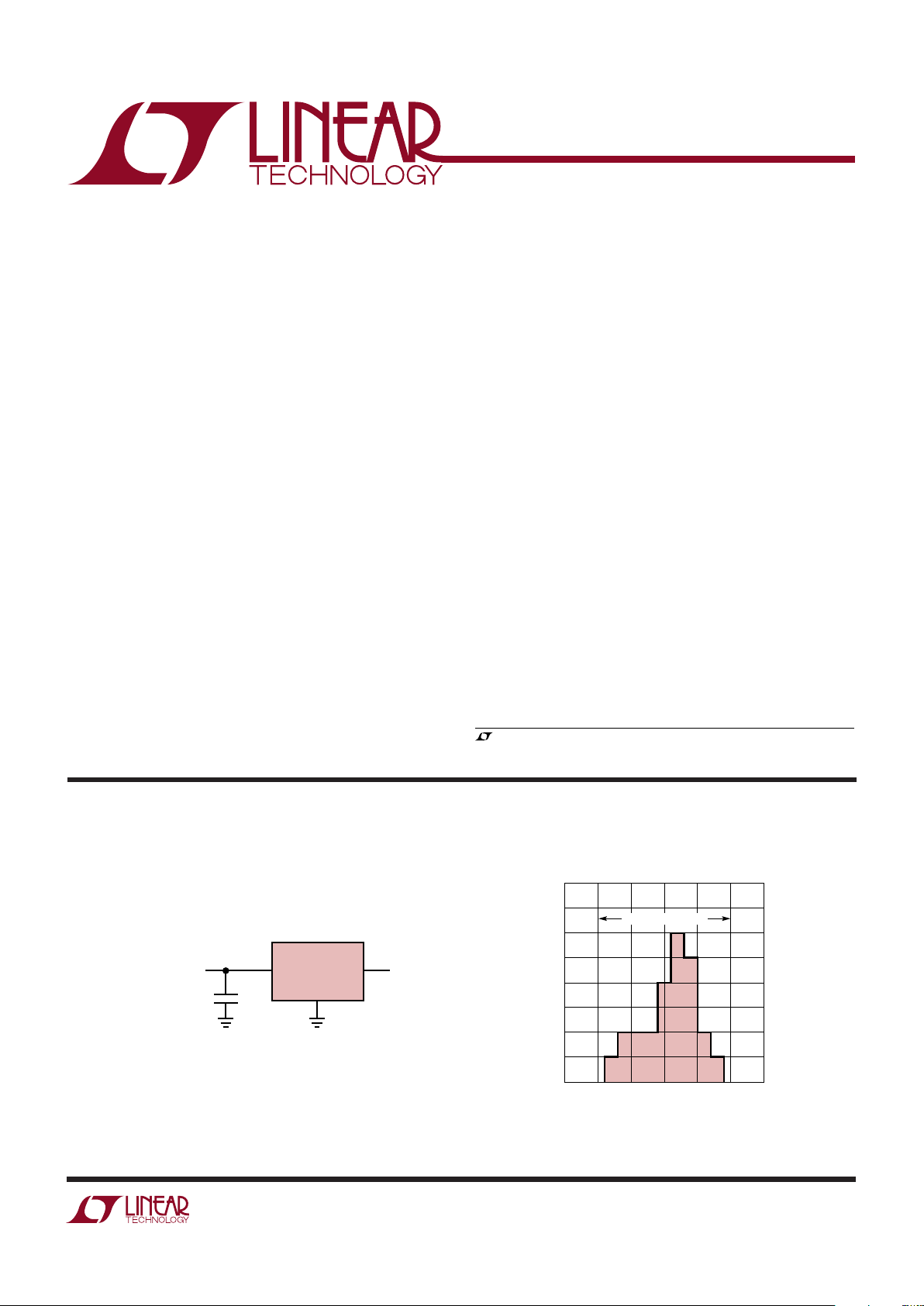
Basic Connection
, LTC and LT are registered trademarks of Linear Technology Corporation.
Typical Distribution of SOT-23 LT1460HC
V
OUT
After
IR Reflow Solder
FEATURES
DESCRIPTIO
U
APPLICATIO S
U
TYPICAL APPLICATIO
U
LT1460S3
GND
IN OUT
V
OUT
+ 0.9V ≤ VIN ≤ 20V
1460S3 TA01
C1
0.1µF
V
OUT
OUTPUT VOLTAGE ERROR (%)
–0.3
DISTRIBUTION (%)
12
16
20
0
0.2
1460S3 TA02
8
4
0
–0.2 –0.1 0.1
24
28
32
0.3
LT1460HC LIMITS
Page 2
2
LT1460S3 (SOT-23)
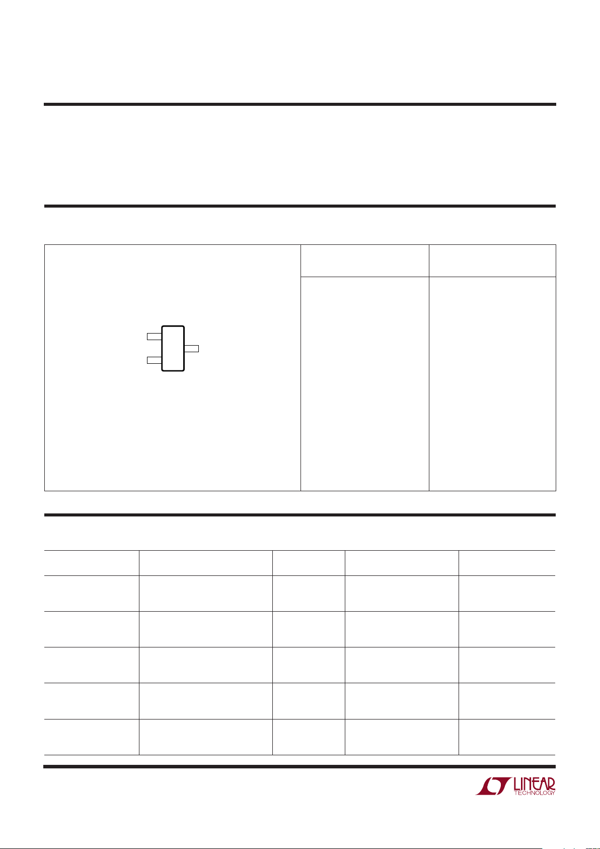
ABSOLUTE MAXIMUM RATINGS
W
WW
U
PACKAGE/ORDER INFORMATION
W
U
U
Input Voltage ........................................................... 30V
Reverse Voltage.................................................... –15V
Output Short-Circuit Duration, TA = 25°C .............. 5 sec
Specified Temperature Range..................... 0°C to 70°C
ORDER PART
NUMBER
S3
PART MARKING
Consult factory for Industrial and Military grade parts.
T
JMAX
= 125°C, θJA = 325°C/W
3 GND
IN 1
TOP VIEW
S3 PACKAGE
3-LEAD PLASTIC SOT-23
OUT 2
LTAC
LTAD
LTAE
LTAN
LTAP
LTAQ
LTAR
LTAS
LTAT
LTAK
LTAL
LTAM
LTAU
LTAV
LTAW
Operating Temperature Range
(Note 2) ............................................. – 40°C to 85°C
Storage Temperature Range (Note 3) ... –65°C to 150°C
Lead Temperature (Soldering, 10 sec)..................300°C
(Note 1)
LT1460HCS3-2.5
LT1460JCS3-2.5
LT1460KCS3-2.5
LT1460HCS3-3
LT1460JCS3-3
LT1460KCS3-3
LT1460HCS3-3.3
LT1460JCS3-3.3
LT1460KCS3-3.3
LT1460HCS3-5
LT1460JCS3-5
LT1460KCS3-5
LT1460HCS3-10
LT1460JCS3-10
LT1460KCS3-10
AVAILABLE OPTIO S
U
OUTPUT VOLTAGE SPECIFIED TEMPERATURE ACCURACY TEMPERATURE PART ORDER
(V) RANGE (%) COEFFICIENT (ppm/°C) NUMBER
2.5 0°C to 70°C 0.2 20 LT1460HCS3-2.5
2.5 0°C to 70°C 0.4 20 LT1460JCS3-2.5
2.5 0°C to 70°C 0.5 50 LT1460KCS3-2.5
30°C to 70°C 0.2 20 LT1460HCS3-3
30°C to 70°C 0.4 20 LT1460JCS3-3
30°C to 70°C 0.5 50 LT1460KCS3-3
3.3 0°C to 70°C 0.2 20 LT1460HCS3-3.3
3.3 0°C to 70°C 0.4 20 LT1460JCS3-3.3
3.3 0°C to 70°C 0.5 50 LT1460KCS3-3.3
50°C to 70°C 0.2 20 LT1460HCS3-5
50°C to 70°C 0.4 20 LT1460JCS3-5
50°C to 70°C 0.5 50 LT1460KCS3-5
10 0°C to 70°C 0.2 20 LT1460HCS3-10
10 0°C to 70°C 0.4 20 LT1460JCS3-10
10 0°C to 70°C 0.5 50 LT1460KCS3-10
Page 3
3
LT1460S3 (SOT-23)
PARAMETER CONDITIONS MIN TYP MAX UNITS
Output Voltage Tolerance (Note 4) LT1460HCS3 –0.2 0.2 %
LT1460JCS3 – 0.4 0.4 %
LT1460KCS3 – 0.5 0.5 %
Output Voltage Temperature Coefficient (Note 5) LT1460HCS3 ● 10 20 ppm/°C
LT1460JCS3
● 10 20 ppm/°C
LT1460KCS3
● 25 50 ppm/°C
Line Regulation V
OUT
+ 0.9V ≤ VIN ≤ V
OUT
+ 2.5V 150 800 ppm/V
● 1000 ppm/V
V
OUT
+ 2.5V ≤ VIN ≤ 20V 50 100 ppm/V
● 130 ppm/V
Load Regulation Sourcing (Note 6) I
OUT
= 100µA 1000 3000 ppm/mA
● 4000 ppm/mA
I
OUT
= 10mA 50 200 ppm/mA
● 300 ppm/mA
I
OUT
= 20mA 20 70 ppm/mA
● 100 ppm/mA
Thermal Regulation (Note 7) ∆P = 200mW 2.5 10 ppm/mW
Dropout Voltage (Note 8) VIN – V
OUT, ∆VOUT
≤ 0.2%, I
OUT
= 0 ● 0.9 V
VIN – V
OUT
, ∆V
OUT
≤ 0.2%, I
OUT
= 10mA 1.3 V
● 1.4 V
Output Current Short V
OUT
to GND 40 mA
Reverse Leakage VIN = –15V ● 0.5 10 µA
Output Voltage Noise (Note 9) 0.1Hz ≤ f ≤ 10Hz 4 ppm (P-P)
10Hz ≤ f ≤ 1kHz 4 ppm (RMS)
Long-Term Stability of Output Voltage (Note 10) 100 ppm/√kHr
Hysteresis (Note 11) ∆T = 0°C to 70°C ● 50 ppm
∆T = –40°C to 85°C
● 250 ppm
Supply Current LT1460S3-2.5 115 145 µA
● 175 µA
LT1460S3-3 145 180 µA
● 220 µA
LT1460S3-3.3 145 180 µA
● 220 µA
LT1460S3-5 160 200 µA
● 240 µA
LT1460S3-10 215 270 µA
● 350 µA
ELECTRICAL CHARACTERISTICS
The ● denotes specifications which apply over the full specified
temperature range, otherwise specifications are at TA = 25°C. VIN = V
OUT
+ 2.5V, I
OUT
= 0 unless otherwise specified.
Note 1: Absolute Maximum Ratings are those values beyond which the life
of a device may be impaired.
Note 2: The LT1460S3 is guaranteed functional over the operating
temperature range of –40°C to 85°C.
Note 3: If the parts are stored outside of the specified temperature range,
the output may shift due to hysteresis.
Note 4: ESD (Electrostatic Discharge) sensitive devices. Extensive use of
ESD protection devices are used internal to the LT1460S3, however, high
electrostatic discharge can damage or degrade the device. Use proper ESD
handling precautions.
Note 5: Temperature coefficient is measured by dividing the change in
output voltage by the specified temperature range. Incremental slope is
also measured at 25°C.
Page 4
4
LT1460S3 (SOT-23)
TYPICAL PERFORMANCE CHARACTERISTICS
UW
2.5V Minimum Input-Output
Voltage Differential 2.5V Load Regulation, Sourcing 2.5V Load Regulation, Sinking
ELECTRICAL CHARACTERISTICS
Note 6: Load regulation is measured on a pulse basis from no load to the
specified load current. Output changes due to die temperature change
must be taken into account separately.
Note 7: Thermal regulation is caused by die temperature gradients created
by load current or input voltage changes. This effect must be added to
normal line or load regulation. This parameter is not 100% tested.
Note 8: Excludes load regulation errors.
Note 9: Peak-to-peak noise is measured with a single pole highpass filter
at 0.1Hz and 2-pole lowpass filter at 10Hz. The unit is enclosed in a still-air
environment to eliminate thermocouple effects on the leads. The test time
is 10 sec. RMS noise is measured with a single pole highpass filter at
10Hz and a 2-pole lowpass filter at 1kHz. The resulting output is full wave
rectified and then integrated for a fixed period, making the final reading an
average as opposed to RMS. A correction factor of 1.1 is used to convert
from average to RMS and a second correction of 0.88 is used to correct
for the nonideal bandpass of the filters.
Note 10: Long-term stability typically has a logarithmic characteristic and
therefore, changes after 1000 hours tend to be much smaller than before
that time. Total drift in the second thousand hours is normally less than
one third that of the first thousand hours with a continuing trend toward
reduced drift with time. Long-term stability will also be affected by
differential stresses between the IC and the board material created during
board assembly.
Note 11: Hysteresis in output voltage is created by package stress that
differs depending on whether the IC was previously at a higher or lower
temperature. Output voltage is always measured at 25°C, but the IC is
cycled to 70°C or 0°C before successive measurements. Hysteresis is
roughly proportional to the square of the temperature change. Hysteresis
is not normally a problem for operational temperature excursions where
the instrument might be stored at high or low temperature. See
Applications Information.
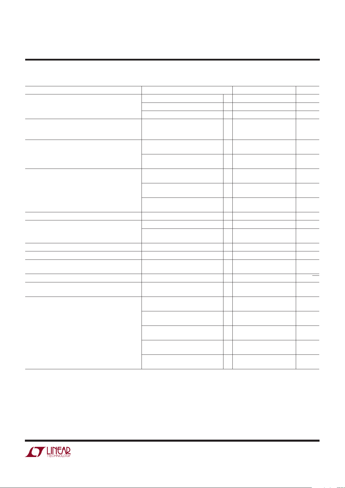
Characteristic curves are similar for most
LT1460S3s. Curves from the LT1460S3-2.5 and the LT1460-10 represent the extremes of the voltage options. Characteristic curves for
other output voltages fall between these curves, and can be estimated based on their voltage output.
INPUT-OUTPUT VOLTAGE (V)
0
0.1
OUTPUT CURRENT (mA)
10
125°C
25°C
100
0.5 1.0 1.5 2.0 2.5
1460S3 G01
1
–55°C
OUTPUT CURRENT (mA)
0.1
–2.0
OUTPUT VOLTAGE CHANGE (mV)
–1.0
0
1 10 100
1460s3 G02
–3.0
–2.5
–1.5
–0.5
–3.5
–4.0
–55°C
25°C
125°C
OUTPUT CURRENT (mA)
0
0
OUTPUT VOLTAGE CHANGE (mV)
20
40
60
80
100
120
1234
–55°C
1460S3 G03
5
125°C
25°C
Page 5

5
LT1460S3 (SOT-23)
FREQUENCY (kHz)
1
OUTPUT IMPEDANCE (Ω)
10
100
1000
0.01 1 10 100
0.1
0.1
1000
1460S3 G08
CL = 0µF
CL = 0.1µF
CL = 1µF
FREQUENCY (kHz)
20
POWER SUPPLY REJECTION RATIO (dB)
40
50
70
80
0.1 10 100 1000
1460S3 G07
0
1
60
30
10
2.5V Output Voltage
Temperature Drift
2.5V Supply Current
vs Input Voltage
2.5V Line Regulation
2.5V Power Supply Rejection
Ratio vs Frequency
2.5V Output Impedance
vs Frequency
2.5V Transient Response
2.5V Output Noise 0.1Hz to 10Hz
TYPICAL PERFORMANCE CHARACTERISTICS
UW
Characteristic curves are similar for most
LT1460S3s. Curves from the LT1460S3-2.5 and the LT1460-10 represent the extremes of the voltage options. Characteristic curves for
other output voltages fall between these curves, and can be estimated based on their voltage output.
20
10
1
0.1
LOAD CURRENT (mA)
200µs/DIV
1460S3 G09
C
LOAD
= 0µF
INPUT VOLTAGE (V)
0
SUPPLY CURRENT (µA)
100
150
125°C
25°C
–55°C
20
1460S3 G05
50
0
5
10
15
250
200
INPUT VOLTAGE (V)
0
OUTPUT VOLTAGE (V)
2.502
2.501
2.500
2.499
2.498
2.497
2.496
2.495
2.494
16
1460S3 G06
4 8 12 20142 6 10 18
25°C
125°C
–55°C
TIME (2 SEC/DIV)
OUTPUT NOISE (20µV/DIV)
1460S3 G11
TEMPERATURE (°C)
–50
OUTPUT VOLTAGE (V)
2.501
2.502
2.503
25 75
1460S3 G04
2.500
2.499
–25 0
50 100 125
2.498
2.497
THREE TYPICAL PARTS
2.5V Output Voltage
Noise Spectrum
FREQUENCY (Hz)
100
1000
10 1k 10k
1460-2.5 G10
100 100k
NOISE VOLTAGE (nV/√Hz)
Page 6

6
LT1460S3 (SOT-23)
TYPICAL PERFORMANCE CHARACTERISTICS
UW
Characteristic curves are similar for most
LT1460S3s. Curves from the LT1460S3-2.5 and the LT1460-10 represent the extremes of the voltage options. Characteristic curves for
other output voltages fall between these curves, and can be estimated based on their voltage output.
10V Minimum Input-Output
Voltage Differential 10V Load Regulation, Sourcing 10V Load Regulation, Sinking
INPUT-OUTPUT VOLTAGE (V)
0
0.1
OUTPUT CURRENT (mA)
10
125°C
25°C
100
0.5 1.0 1.5 2.0 2.5
1460S3 G12
1
–55°C
OUTPUT CURRENT (mA)
0.1
15
OUTPUT VOLTAGE CHANGE (mV)
20
25
30
35
1 10 100
1460S3 G13
10
5
–5
–10
0
125°C 25°C
–55°C
OUTPUT CURRENT (mA)
0
OUTPUT VOLTAGE CHANGE (mV)
150
200
250
4
1460S3 G14
100
50
0
1
2
3
5
125°C
–55°C
25°C
10V Output Voltage
Temperature Drift
10V Supply Current
vs Input Voltage
10V Line Regulation
TEMPERATURE (°C)
–50
OUTPUT VOLTAGE (V)
10.002
10.004
10.006
0
50
75
1460S3 G15
9.998
10.000
9.996
9.994
9.992
9.990
9.988
9.986
9.984
9.982
–25
25
100
125
THREE TYPICAL PARTS
INPUT VOLTAGE (V)
0
0
SUPPLY CURRENT (µA)
50
150
200
250
350
2
10
14
1460S3 G16
100
300
8
18
20
4
6
12 16
125°C
–55°C
25°C
INPUT VOLTAGE (V)
6
OUTPUT VOLTAGE (V)
10.000
10.005
10.010
12 16
1560S3 G17
9.995
9.990
810
14 18 20
9.985
9.980
125°C
–55°C
25°C
10V Power Supply Rejection
Ratio vs Frequency
10V Output Impedance
vs Frequency
10V Transient Response
FREQUENCY (kHz)
30
POWER SUPPLY REJECTION RATIO (dB)
90
100
20
10
80
50
70
60
40
0.1 10 100 1000
1460S3 G18
0
1
FREQUENCY (kHz)
1
OUTPUT IMPEDANCE (Ω)
10
100
1000
0.01 1 10 100
0.1
0.1
1000
1460S3 G19
CL = 0µF
CL = 0.1µF
CL = 1µF
20
10
1
0.1
LOAD CURRENT (mA)
200µs/DIV
1460S3 G20
C
LOAD
= 0µF
Page 7

7
LT1460S3 (SOT-23)
APPLICATIONS INFORMATION
WUU
U
Longer Battery Life
Series references have a large advantage over older shunt
style references. Shunt references require a resistor from
the power supply to operate. This resistor must be chosen
to supply the maximum current that can ever be
demanded by the circuit being regulated. When the circuit
being controlled is not operating at this maximum current,
the shunt reference must always sink this current, resulting in high dissipation and short battery life.
The LT1460S3 series references do not require a current
setting resistor and can operate with any supply voltage
from V
OUT
+ 0.9V to 20V. When the circuitry being regulated does not demand current, the LT1460S3s reduce
their dissipation and battery life is extended. If the references are not delivering load current, they dissipate only
several mW, yet the same connection can deliver 20mA of
load current when demanded.
Capacitive Loads
The LT1460S3 family of references are designed to be
stable with a large range of capacitive loads. With no
TYPICAL PERFORMANCE CHARACTERISTICS
UW
Characteristic curves are similar for most
LT1460S3s. Curves from the LT1460S3-2.5 and the LT1460-10 represent the extremes of the voltage options. Characteristic curves for
other output voltages fall between these curves, and can be estimated based on their voltage output.
10V Output Noise 0.1Hz to 10Hz
TIME (2 SEC/DIV)
OUTPUT NOISE (20µV/DIV)
1460S3 G22
capacitive load, these references are ideal for fast settling
or applications where PC board space is a premium. The
test circuit shown in Figure 1 is used to measure the
response time and stability of various load currents and
load capacitors. This circuit is set for the 2.5V option. For
other voltage options, the input voltage must be scaled up
and the output voltage generator offset voltage must be
adjusted. The 1V step from 2.5V to 1.5V produces a
current step of 10mA or 1mA for RL = 100Ω or RL = 1k.
Figure 2 shows the response of the reference to these 1mA
and 10mA load steps with no load capacitance, and Figure
3 shows a 1mA and 10mA load step with a 0.1µF output
capacitor. Figure 4 shows the response to a 1mA load step
with CL = 1µF and 4.7µF.
LT1460S3-2.5
R
L
V
OUT
V
GEN
1460S3 F01
C
IN
0.1µF
2.5V
1.5V
C
L
VIN = 2.5V
Figure 1. Response Time Test Circuit
10V Output Voltage
Noise Spectrum
FREQUENCY (kHz)
0.01
0.1
1
10
1100.1 100
1460S3 G10
NOISE VOLTAGE (µV/√Hz)
Page 8

8
LT1460S3 (SOT-23)
100µs/DIV
V
GEN
V
OUT
V
OUT
1460S3 F02
2.5V
1.5V
1mA
10mA
1µs/DIV
Figure 2. CL = 0µF
V
GEN
V
OUT
1460S3-5 F03
2.5V
1.5V
1mA
10mA
Figure 3. CL = 0.1µF
V
GEN
1460S3 F04
2.5V
1.5V
1µF
100µs/DIV
Figure 4. I
OUT
= 1mA
V
OUT
4.7µF
V
OUT
V
OUT
APPLICATIONS INFORMATION
WUU
U
Table 1 gives the maximum output capacitance for various
load currents and output voltages to avoid instability. Load
capacitors with low ESR (effective series resistance) cause
more ringing than capacitors with higher ESR such as
polarized aluminum or tantalum capacitors.
Table 1. Maximum Output Capacitance
VOLTAGE
OPTION I
OUT
= 100µAI
OUT
= 1mA I
OUT
= 10mA I
OUT
= 20mA
2.5V >10µF>10µF2µF 0.68µF
3V >10µF>10µF2µF 0.68µF
3.3V >10µF>10µF1µF 0.68µF
5V >10µF>10µF1µF 0.68µF
10V >10µF1µF 0.15µF 0.1µF
Long-Term Drift
Long-term drift cannot be extrapolated from acceler-
ated high temperature testing. This erroneous technique gives drift numbers that are widely optimistic. The
only way long-term drift can be determined is to measure it over the time interval of interest. The LT1460S3
long-term drift data was taken on over 100 parts that were
soldered into PC boards similar to a “real world” application. The boards were then placed into a constant temperature oven with TA = 30°C, their outputs were scanned
regularly and measured with an 8.5 digit DVM. Figure 5
shows typical long-term drift of the LT1460S3s.
HOURS
–150
ppm
–50
50
150
–100
0
100
200 400 600 800
1460S3 F05
10001000 300 500 700 900
Figure 5. Typical Long-Term Drift
Page 9

9
LT1460S3 (SOT-23)
APPLICATIONS INFORMATION
WUU
U
Hysteresis
Hysteresis data shown in Figure 5 and Figure 6 represents
the worst-case data taken on parts from 0°C to 70°C and
from – 40°C to 85°C. The output is capable of dissipating
relatively high power, i.e., for the LT1460S3-2.5, PD =
17.5V • 20mA = 350mW. The thermal resistance of the
SOT-23 package is 325°C/W and this dissipation causes
a 114°C internal rise producing a junction temperature of
TJ = 25°C + 114°C = 139°C. This elevated temperature will
cause the output to shift due to thermal hysteresis. For
highest performance in precision applications, do not
let the LT1460S3’s junction temperature exceed 85°C.
Fast Turn-On
It is recommended to add a 0.1µF or larger bypass
capacitor to the input pin of the LT1460S3s. Although this
can help stability with large load currents, another reason
is for proper start-up. The LT1460S3 can start in 10µs, but
it is important to limit the dv/dt of the input. Under light
load conditions and with a very fast input, internal nodes
overslew and this requires finite recovery time. Figure 8
shows the result of no bypass capacitance on the input and
no output load on the LT1460S3-5. In this case the supply
dv/dt is 7.5V in 30ns which causes internal overslew, and
the output does not bias to 5V until 40µs after turn-on.
Although 40µs is a typical turn-on time, it can be much
longer. Figure 9 shows the effect of a 0.1µF bypass
capacitor which limits the input dv/dt to approximately
7.5V in 20µs. The part always starts quickly.
Figure 6. 0°C to 70°C Hysteresis
Figure 7. –40°C to 85°C Hysteresis
V
IN
20µs/DIV
Figure 8. CIN = 0µF
0V
V
OUT
0V
7.5V
1460S3 F08
V
IN
20µs/DIV
Figure 9. CIN = 0.1µF
V
OUT
0V
7.5V
1460S3 F08
HYSTERESIS (ppm)
–240 –160 –80 0
NUMBER OF UNITS
8
70°C TO 25°C0°C TO 25°C
10
12
1460S3 F06
6
4
80
160
–200 –120 –40 40
120
200
2
0
18
16
14
240
WORST-CASE HYSTERESIS
ON 40 UNITS
HYSTERESIS (ppm)
–600 –400 –200 0
NUMBER OF UNITS
4
85°C TO 25°C–40°C TO 25°C
5
6
1460S3 F07
3
2
200
400
–500 –300 –100 100
300
500
1
0
9
8
7
600
WORST-CASE HYSTERESIS
ON 34 UNITS
Page 10

10
LT1460S3 (SOT-23)
APPLICATIONS INFORMATION
WUU
U
Output Accuracy
Like all references, either series or shunt, the error budget
of the LT1460S3s is made up of primarily three components: initial accuracy, temperature coefficient and load
regulation. Line regulation is neglected because it typically
contributes only 150ppm/V. The LT1460S3s typically
shift 0.02% when soldered into a PCB, so this is also
neglected. The output errors are calculated as follows for
a 100µA load and 0°C to 70°C temperature range:
LT1460HCS3
Initial Accuracy = 0.2%
For I
OUT
= 100µA
∆V
OUT
= (4000ppm/mA)(0.1mA) = 0.04%
For Temperature 0°C to 70°C the maximum ∆T = 70°C
∆V
OUT
= (20ppm/°C)(70°C) = 0.14%
Total worst-case output error is:
0.2% + 0.04% + 0.14% = 0.380%
Table 2 gives the worst-case accuracy for LT1460HCS3,
LT1460JCS3 and LT1460KCS3 from 0°C to 70°C, and
shows that if the LT1460HCS3 is used as a reference
instead of a regulator, it is capable of 8 bits of absolute
accuracy over temperature without a system calibration.
Table 2. Worst-Case Output Accuracy over Temperature
I
OUT
LT1460HCS3 LT1460JCS3 LT1460KCS3
0µA 0.340% 0.540% 0.850%
100µA 0.380% 0.580% 0.890%
10mA 0.640% 0.840% 1.15%
20mA 0.540% 0.740% 1.05%
Page 11

11
LT1460S3 (SOT-23)
Information furnished by Linear Technology Corporation is believed to be accurate and reliable.
However, no responsibility is assumed for its use. Linear Technology Corporation makes no representation that the interconnection of its circuits as described herein will not infringe on existing patent rights.
Dimensions in millimeters (inches) unless otherwise noted.
PACKAGE DESCRIPTION
U
S3 Package
3-Lead Plastic SOT-23
(LTC DWG # 05-08-1631)
0.95
0.037
BSC
1.20 – 1.40
(0.047 – 0.060)
0.55
(0.022)
0.37 – 0.51
(0.015 – 0.020)
SOT-23 0599
2.80 – 3.04
(0.110 – 0.120)
1.92
0.075
BSC
0.89 – 1.12
(0.035 – 0.044)
0.013 – 0.10
(0.0005 – 0.004)
0.09 – 0.18
(0.004 – 0.007)
0.45 – 0.60
(0.017 – 0.024)
2.10 – 2.64
(0.083 – 0.104)
REF
NOTE:
1. DIMENSIONS ARE IN MILLIMETERS
2. DIMENSIONS ARE INCLUSIVE OF PLATING
3. DIMENSIONS ARE EXCLUSIVE OF MOLD FLASH AND METAL BURR
4. MOLD FLASH SHALL NOT EXCEED 0.254mm
5. JEDEC REFERENCE IS TO-236 VARIATION AB
Page 12

12
LT1460S3 (SOT-23)
1460s3f LT/TP 0999 4K • PRINTED IN USA
LINEAR TECHNOLOGY CORPORATION 1997
Linear Technology Corporation
1630 McCarthy Blvd., Milpitas, CA 95035-7417 ● (408) 432-1900
FAX: (408) 434-0507
●
TELEX: 499-3977 ● www.linear-tech.com
Handling Higher Load Currents
Boosted Output Current with No Current Limit Boosted Output Current with Current Limit
RELATED PARTS
PART NUMBER DESCRIPTION COMMENTS
LT1019 Precision Bandgap Reference 0.05% Max, 5ppm/°C Max
LT1027 Precision 5V Reference 0.02%, 2ppm/°C Max
LT1236 Precision Low Noise Reference 0.05% Max, 5ppm/°C Max, SO Package
LT1461 Micropower Precision Low Dropout 0.04% Max, 3ppm/°C Max, 50mA Output Current
LT1634 Micropower Precision Shunt Reference 1.25V, 2.5V Output 0.05%, 25ppm/°C Max
LTC1798 Micropower Low Dropout Reference, Fixed or Adjustable 0.15% Max, 40ppm/°C, 6.5µA Max Supply Current
TYPICAL APPLICATIONS
U
1460S3 TA05
R
L
40mA
V
+
R1*
V
OUT
TYPICAL LOAD
CURRENT = 50mA
SELECT R1 TO DELIVER 80% OF TYPICAL LOAD CURRENT.
LT1460 WILL THEN SOURCE AS NECESSARY TO MAINTAIN
PROPER OUTPUT. DO NOT REMOVE LOAD AS OUTPUT WILL
BE DRIVEN UNREGULATED HIGH. LINE REGULATION IS
DEGRADED IN THIS APPLICATION
*
10mA
47µF
+
LT1460S3
OUT
GND
IN
R1 =
V
+
– V
OUT
40mA
V+ ≥ (V
OUT
+ 1.8V)
LT1460S3
OUT
GND
IN
1460S3 TA03
2N2905
V
OUT
100mA
47µF
2µF
SOLID
TANT
R1
220Ω
+
+
1460S3 TA04
2N2905
V
OUT
100mA
2µF
SOLID
TANT
D1*
LED
V+ ≥ V
OUT
+ 2.8V
8.2Ω
R1
220Ω
GLOWS IN CURRENT LIMIT,
DO NOT OMIT
*
47µF
+
+
LT1460S3
OUT
GND
IN
 Loading...