

Page 1
1
LT1460-10
Micropower Precision
Series Reference
FEATURES
DESCRIPTION
U
■
High Accuracy: 0.075% Max
■
Low Drift: 10ppm/°C Max
■
Industrial Temperature Range SO-8 Package
■
Low Supply Current: 270µA Max
■
Minimum Output Current: 20mA
■
No Output Capacitor Required
■
Reverse Battery Protection
■
Minimum Input/Output Differential: 0.9V
■
Available in Small MSOP Package
The LT®1460-10 is a micropower bandgap reference that
combines very high accuracy and low drift with low power
dissipation and small package size. This series reference
uses curvature compensation to obtain a low temperature
coefficient and trimmed precision thin-film resistors to
achieve high output accuracy. The reference will supply up to
20mA, making it ideal for precision regulator applications, yet
it is almost totally immune to input voltage variations.
This series reference provides supply current and power
dissipation advantages over shunt references that must idle
the entire load current to operate. Additionally, the LT1460-10
does not require an output capacitor, but it is stable with
capacitive loads. This feature is important in critical applications where PC board space is a premium or fast settling is
demanded. Reverse battery protection keeps the reference
from conducting current and being damaged.
The LT1460-10 is available in the 8-lead MSOP, SO, PDIP
and the 3-lead TO-92 packages. It is also available in the
SOT-23 package; see separate data sheet LT1460S3-10
(SOT-23).
APPLICATIONS
U
■
Handheld Instruments
■
Precision Regulators
■
A/D and D/A Converters
■
Power Supplies
■
Hard Disk Drives
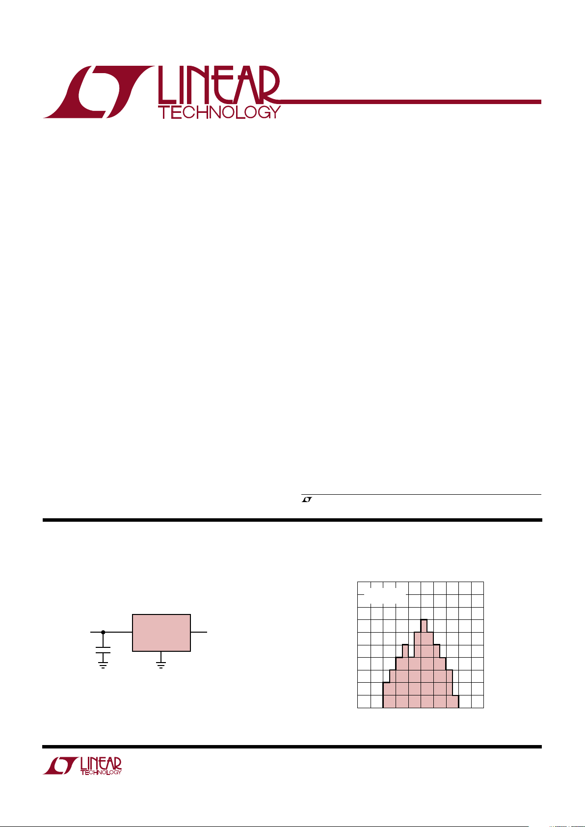
Typical Distribution of Output Voltage
S8 Package
, LTC and LT are registered trademarks of Linear Technology Corporation.
TYPICAL APPLICATION
U
OUTPUT VOLTAGE ERROR (%)
–0.10
UNITS (%)
–0.06
–0.02 0
1460-10 TA02
0.060.02
20
18
16
14
12
10
8
6
4
2
0
0.10
1400 PARTS
FROM 2 RUNS
Basic Connection
LT1460-10
GND
IN OUT
1460-10 TA01
C1
0.1µF
10V
10.9V
TO 20V
Page 2
2
LT1460-10
ABSOLUTE MAXIMUM RATINGS
W
WW
U
Input Voltage ........................................................... 30V
Reverse Voltage.................................................... – 15V
Output Short-Circuit Duration, TA = 25°C ............. 5 sec
Specified Temperature Range
Commercial ............................................ 0°C to 70°C
Industrial ........................................... – 40°C to 85°C
Storage Temperature Range (Note 1) ... –65°C to 150°C
Lead Temperature (Soldering, 10 sec).................. 300°C
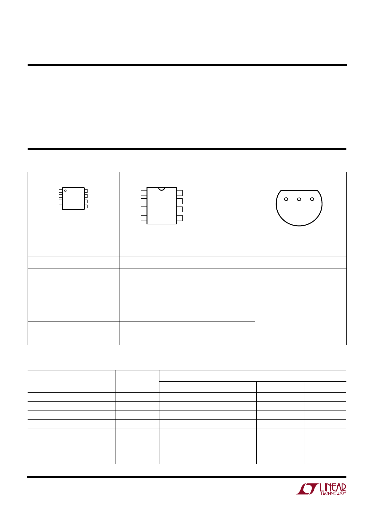
Available Options
TEMPERATURE
PACKAGE TYPE
ACCURACY COEFFICIENT
TEMPERATURE (%) (ppm/
°
C)
N8 S8 MS8 Z
0°C to 70°C 0.075 10 LT1460ACN8-10 LT1460ACS8-10
–40°C to 85°C 0.10 10 LT1460BIN8-10 LT1460BIS8-10
0°C to 70°C 0.10 15 LT1460CCMS8-10
0°C to 70°C 0.10 20 LT1460DCN8-10 LT1460DCS8-10
–40°C to 85°C 0.125 20 LT1460EIN8-10 LT1460EIS8-10
0°C to 70°C 0.15 25 LT1460FCMS8-10
0°C to 70°C 0.25 25 LT1460GCZ-10
–40°C to 85°C 0.25 25 LT1460GIZ-10
PACKAGE/ORDER INFORMATION
W
U
U
1
2
3
4
NC*
V
IN
NC*
GND
8
7
6
5
NC*
NC*
V
OUT
NC*
TOP VIEW
MS8 PACKAGE
8-LEAD PLASTIC MSOP
*CONNECTED INTERNALLY.
DO NOT CONNECT EXTERNAL
CIRCUITRY TO THESE PINS
MS8 PART MARKING
ORDER PART NUMBERORDER PART NUMBERORDER PART NUMBER
S8 PART MARKING
1460A1
460BI1
LTAH
LTAJ
1460D1
460EI1
T
JMAX
= 150°C, θJA = 250°C/W
1
2
3
4
8
7
6
5
TOP VIEW
NC*
V
IN
NC*
GND
NC*
NC*
V
OUT
NC*
N8 PACKAGE
8-LEAD PDIP
S8 PACKAGE
8-LEAD PLASTIC SO
*CONNECTED INTERNALLY.
DO NOT CONNECT
EXTERNAL CIRCUITRY
TO THESE PINS
T
JMAX
= 150°C, θJA = 130°C/ W (N8)
T
JMAX
= 150°C, θJA = 190°C/ W (S8)
12
3
BOTTOM VIEW
V
INVOUT
GND
Z PACKAGE
3-LEAD TO-92 PLASTIC
T
JMAX
= 150°C, θJA = 160°C/ W
LT1460CCMS8-10
LT1460FCMS8-10
LT1460ACS8-10
LT1460BIS8-10
LT1460DCS8-10
LT1460EIS8-10
LT1460ACN8-10
LT1460BIN8-10
LT1460DCN8-10
LT1460EIN8-10
LT1460GCZ-10
LT1460GIZ-10
Consult factory for Military grade parts.
Page 3
3
LT1460-10
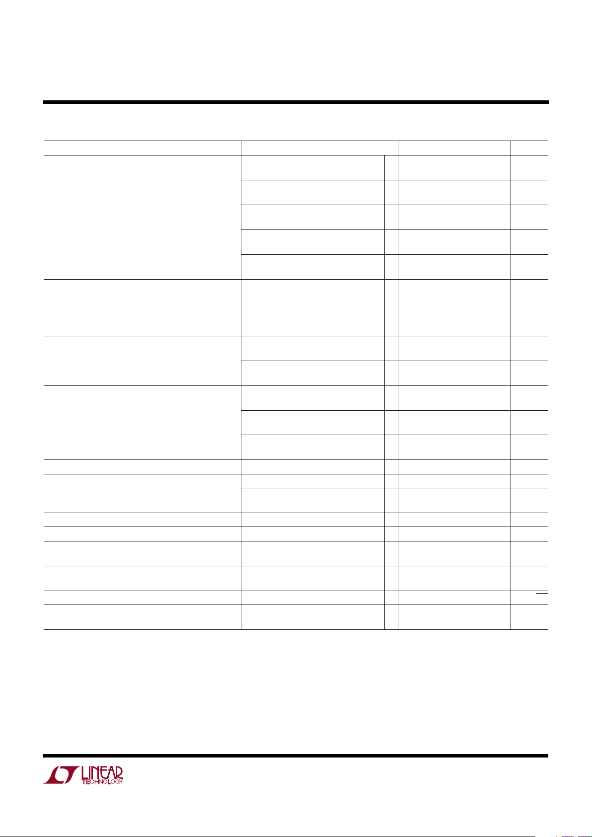
PARAMETER CONDITIONS MIN TYP MAX UNITS
Output Voltage (Note 2) LT1460ACN8, ACS8 9.9925 10.000 10.0075 V
–0.075 0.075 %
LT1460BIN8, BIS8, CCMS8, DCN8, DCS8 9.990 10.000 10.010 V
–0.10 0.10 %
LT1460EIN8, EIS8 9.9875 10.000 10.0125 V
–0.125 0.125 %
LT1460FCMS8 9.985 10.000 10.015 V
–0.15 0.15 %
LT1460GCZ, GIZ 9.975 10.000 10.025 V
–0.25 0.25 %
Output Voltage Temperature Coefficient (Note 3) T
MIN
≤ TJ ≤ T
MAX
LT1460ACN8, ACS8, BIN8, BIS8 ● 5 10 ppm/°C
LT1460CCMS8
● 7 15 ppm/°C
LT1460DCN8, DCS8, EIN8, EIS8
● 10 20 ppm/°C
LT1460FCMS8, GCZ, GIZ
● 12 25 ppm/°C
Line Regulation 10.9V ≤ VIN ≤ 12.5V 30 60 ppm/V
● 80 ppm/V
12.5V ≤ VIN ≤ 20V 10 25 ppm/V
● 35 ppm/V
Load Regulation Sourcing (Note 4) I
OUT
= 100µA 1500 2800 ppm/mA
● 3500 ppm /mA
I
OUT
= 10mA 80 135 ppm/mA
● 180 ppm/mA
I
OUT
= 20mA 70 100 ppm/mA
0°C to 70°C
● 140 ppm/mA
Thermal Regulation (Note 5) ∆P = 200mW 0.5 2.5 ppm/mW
Dropout Voltage (Note 6) VIN – V
OUT
, ∆V
OUT
≤ 0.1%, I
OUT
= 0 ● 0.9 V
VIN – V
OUT
, ∆V
OUT
≤ 0.1%, I
OUT
= 10mA 1.3 V
● 1.4 V
Output Current Short V
OUT
to GND 40 mA
Reverse Leakage VIN = –15V ● 0.5 10 µA
Supply Current 190 270 µA
● 360 µA
Output Voltage Noise (Note 7) 0.1Hz ≤ f ≤ 10Hz 40 µV
P-P
10Hz ≤ f ≤ 1kHz 35 µV
RMS
Long-Term Stability of Output Voltage, S8 Pkg (Note 8) 40 ppm/√kHr
Hysteresis (Note 9) ∆T = –40°C to 85°C 160 ppm
∆T = 0°C to 70°C 25 ppm
The ● denotes specifications which apply over the specified temperature
range.
Note 1: If the part is stored outside of the specified temperature range, the
output may shift due to hysteresis.
Note 2: ESD (Electrostatic Discharge) sensitive device. Extensive use of
ESD protection devices are used internal to the LT1460-10, however, high
electrostatic discharge can damage or degrade the device. Use proper ESD
handling precautions.
Note 3: Temperature coefficient is measured by dividing the change in
output voltage by the specified temperature range. Incremental slope is
also measured at 25°C.
Note 4: Load regulation is measured on a pulse basis from no load to the
specified load current. Output changes due to die temperature change
must be taken into account separately.
Note 5: Thermal regulation is caused by die temperature gradients created
by load current or input voltage changes. This effect must be added to
normal line or load regulation. This parameter is not 100% tested.
ELECTRICAL CHARACTERISTICS
VIN = 12.5V, I
OUT
= 0, TA = 25°C unless otherwise specified.
Page 4
4
LT1460-10
ELECTRICAL CHARACTERISTICS
Note 6: Excludes load regulation errors.
Note 7: Peak-to-peak noise is measured with a single highpass filter at
0.1Hz and a 2-pole lowpass filter at 10Hz. The unit is enclosed in a still-air
environment to eliminate thermocouple effects on the leads. The test time
is 10 sec. RMS noise is measured with a single highpass filter at 10Hz and
a 2-pole lowpass filter at 1kHz. The resulting output is full wave rectified
and then integrated for a fixed period, making the final reading an average
as opposed to RMS. A correction factor of 1.1 is used to convert from
average to RMS and a second correction of 0.88 is used to correct for the
nonideal bandpass of the filters.
Note 8: Long-term stability typically has a logarithmic characteristic and
therefore, changes after 1000 hours tend to be much smaller than before
that time. Total drift in the second thousand hours is normally less than
one third that of the first thousand hours with a continuing trend toward
reduced drift with time. Significant improvement in long-term drift can be
realized by preconditioning the IC with a 100 hour to 200 hour, 125°C
burn-in. Long-term stability will also be affected by differential stresses
between the IC and the board material created during board assembly. See
PC Board Layout in the Applications Information section.
Note 9: Hysteresis in output voltage is created by package stress that
differs depending on whether the IC was previously at a higher or lower
temperature. Output voltage is always measured at 25°C, but the IC is
cycled to 85°C or –40°C before successive measurements. Hysteresis is
roughly proportional to the square of the temperature change. Hysteresis
is not normally a problem for operational temperature excursions where
the instrument might be stored at high or low temperature.
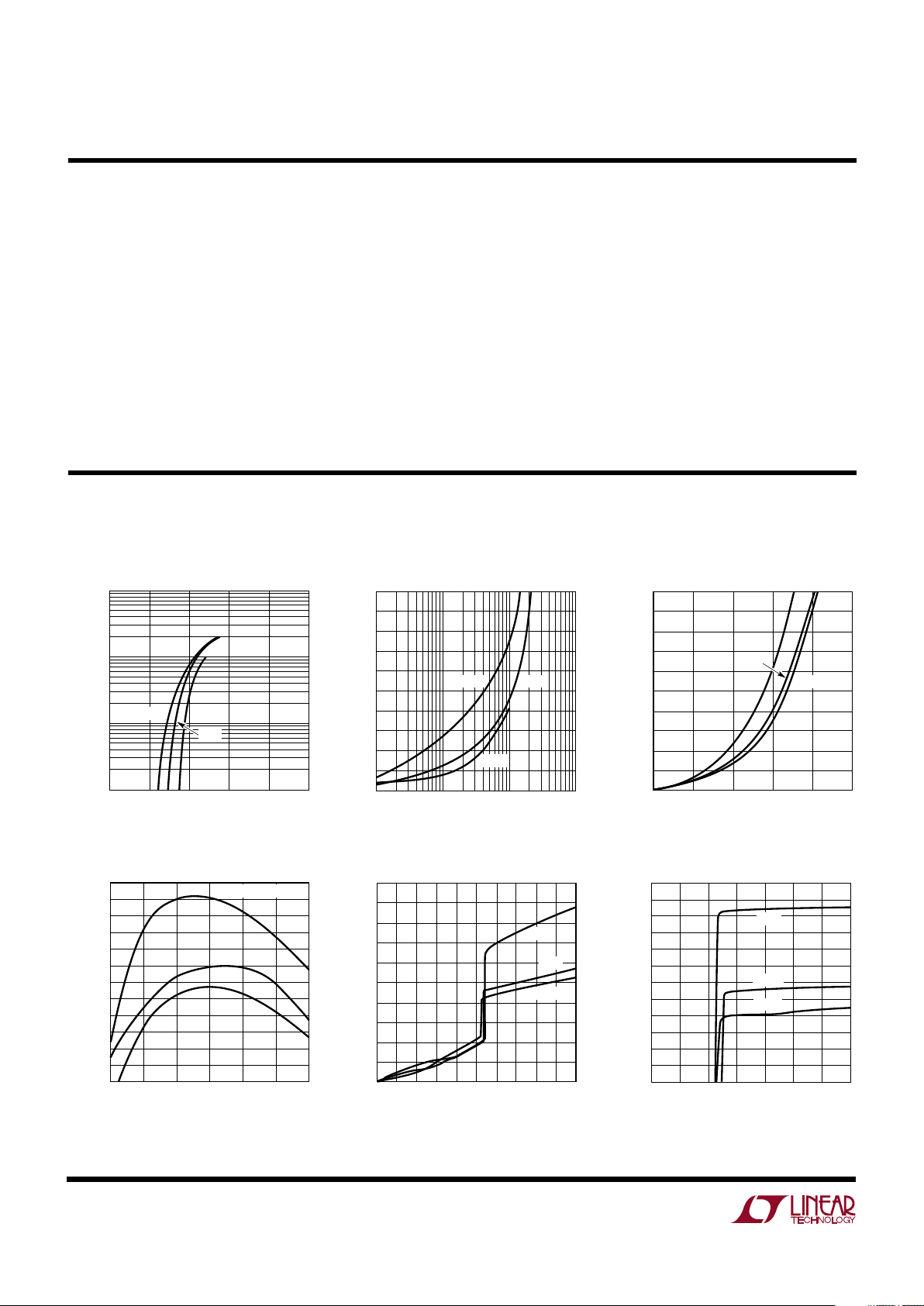
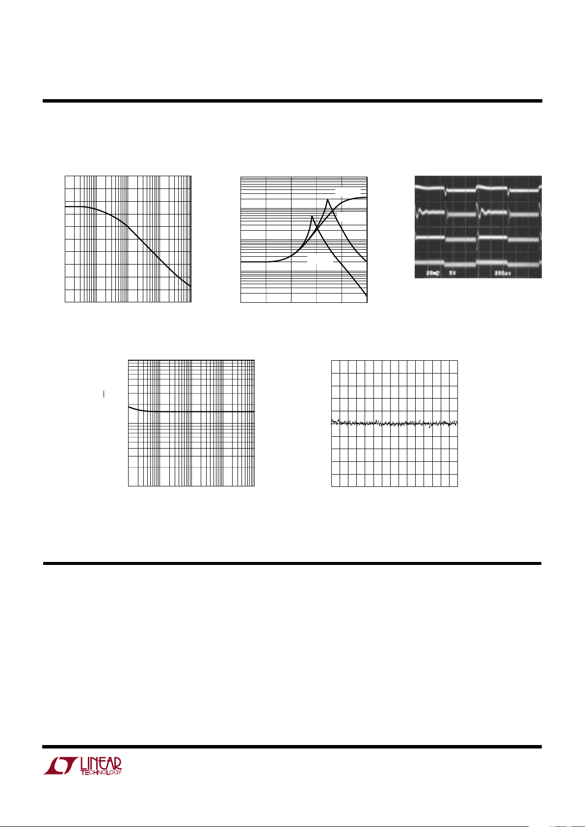
TYPICAL PERFORMANCE CHARACTERISTICS
UW
OUTPUT CURRENT (mA)
0
OUTPUT VOLTAGE CHANGE (mV)
60
80
100
4
1460-10 G03
40
20
50
70
90
30
10
0
1
2
3
5
–55°C
125°C
25°C
Load Regulation, Sinking
Line Regulation
TEMPERATURE (°C)
–50
9.982
OUTPUT VOLTAGE (V)
9.986
9.990
9.994
9.998
10.006
–25
02550
1460-10 G04
75 100
10.002
3 TYPICAL PARTS
Output Voltage Temperature Drift
INPUT/OUTPUT VOLTAGE (V)
0
0.1
OUTPUT CURRENT (mA)
100
0.5 1.0 1.5 2.0 2.5
1460-10 G01
10
1
–55°C
125°C
25°C
Minimum Input/Output
Voltage Differential
INPUT VOLTAGE (V)
6
9.980
OUTPUT VOLTAGE (V)
9.984
9.988
9.992
9.996
10.004
10
14 18
1460-10 G06
8
12
16 20
10.000
–55°C
125°C
25°C
Supply Current vs Input Voltage
INPUT VOLTAGE (V)
0
SUPPLY CURRENT (µA)
240
320
400
16
1460-10 G05
160
80
200
280
360
120
40
0
4
8
12
218
6
10
14
20
–55°C
125°C
25°C
OUTPUT CURRENT (mA)
0.1
4
OUTPUT VOLTAGE CHANGE (mV)
5
6
7
8
1 10 100
1460-10 G02
3
2
1
0
9
10
–55°C
25°C125°C
Load Regulation, Sourcing
Page 5
5
LT1460-10
TYPICAL PERFORMANCE CHARACTERISTICS
UW
Power Supply Rejection Ratio
vs Frequency Transient Responses
10
1
0.1
0
200µs/DIV
LOAD CAPACITANCE (µF)
I
OUT
= 10mA
1460-10 G09
Output Impedance vs Frequency
FREQUENCY (kHz)
1
OUTPUT IMPEDANCE (Ω)
10
100
1000
0.01 1 10 100
0.1
0.1
1000
1460-10 G08
CL = 0µF
CL = 1µF
CL = 0.1µF
Output Voltage Noise Spectrum
FREQUENCY (kHz)
0.01
0.1
1
10
1100.1 100
1460-10 G10
NOISE VOLTAGE (µV/√Hz)
Output Noise 0.1Hz to 10Hz
TIME (SEC)
0
OUTPUT NOISE (50µV/DIV)
8
1460-10 G11
2
4
6
10
12
14
APPLICATIONS INFORMATION
WUU
U
Precision Regulator
The LT1460-10 is ideal as a precision regulator, and since
it operates in series mode it does not require a current
setting resistor. The reference can supply up to 20mA of
load current with good transient response. Load regulation at 20mA output is typically 70ppm/mA meaning the
output changes only 14mV.
Capacitive Loads
The LT1460-10 is designed to be stable with capacitive
loads. With no capacitive load, the reference is ideal for
fast settling or applications where PC board space is a
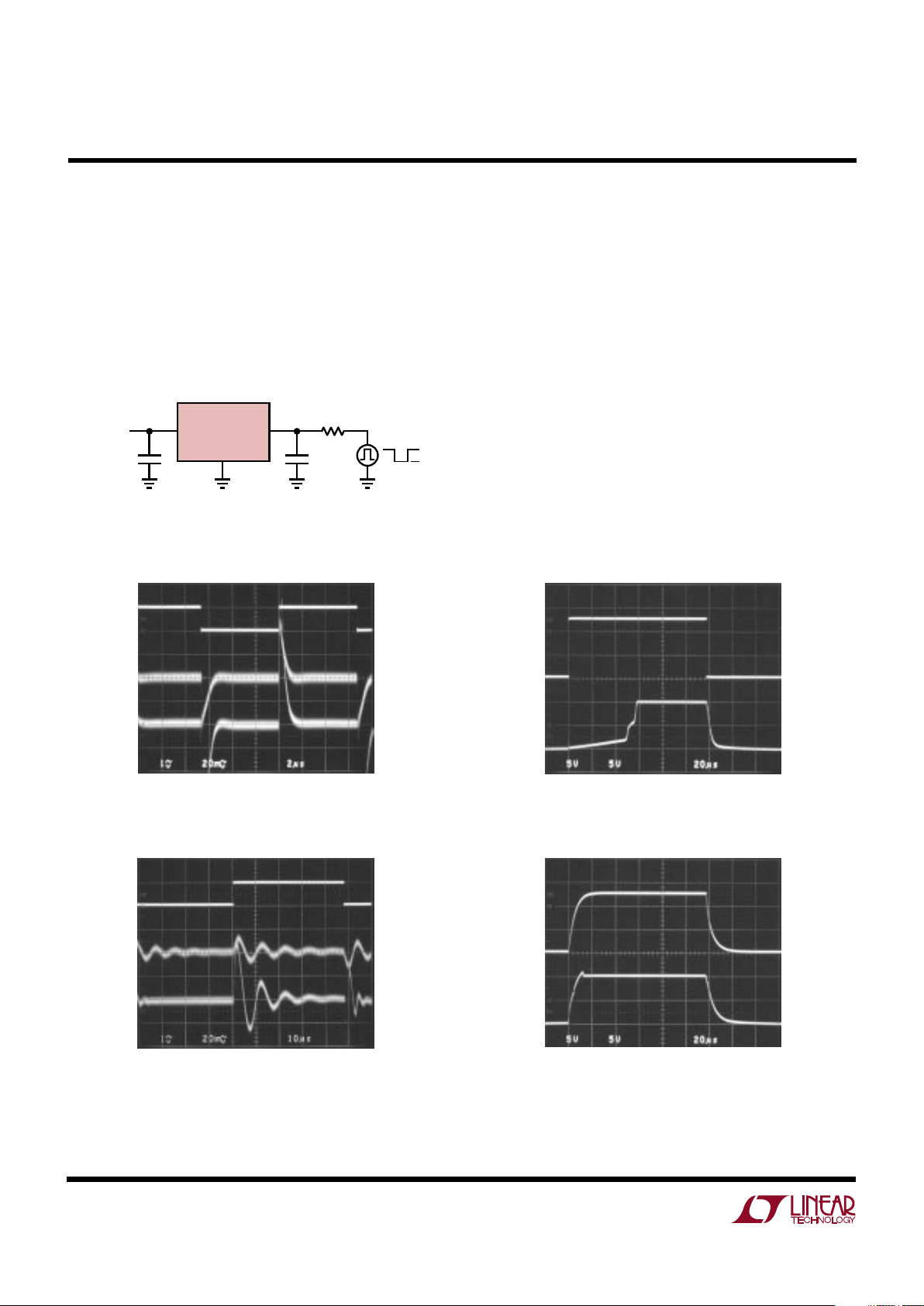
premium. The test circuit shown in Figure 1 is used to
measure the response time for various load currents and
load capacitors. The 1V step from 10V to 9V produces a
INPUT FREQUENCY (kHz)
20
POWER SUPPLY REJECTION RATIO (dB)
40
60
50
80
100
10
30
70
90
0.1 10 100 1000
1460-10 G07
0
1
Page 6
6
LT1460-10
APPLICATIONS INFORMATION
WUU
U
current step of 1mA or 100µA for RL = 1k or RL = 10k.
Figure 2 shows the response of the reference with no load
capacitance.
The reference settles to 10mV (0.1%) in 0.4µ s for a 100µ A
pulse and to 0.1% in 0.8µs with a 1mA step. When load
capacitance is greater than 0.01µ F, the reference begins to
ring due to the pole formed with the output impedance.
Figure 3 shows the response of the reference to a 1mA and
100µ A load with a 0.01µF load capacitor.
Fast Turn-On
It is recommended to add a 0.1µ F or larger input capacitor
to the input pin of the LT1460-10. This helps stability with
large load currents and speeds up turn-on. The LT1460-10
can start in 10µ s, but it is important to limit the dv/dt of the
input. Under light load conditions and with a very fast
input, internal nodes overslew and this requires finite
recovery time. Figure 4 shows the result of no bypass
capacitance on the input and no output load. In this case
the supply dv/dt is 12.5V in 30ns which causes internal
overslew, and the output does not bias to 10V until 60µs.
A 0.1µ F input capacitor guarantees the part always starts
quickly as shown in Figure 5.
Figure 3. CL = 0.01µF
10µs/DIV 1460-10 F03
2µs/DIV 1460-10 F02
10V
9V
Figure 2. CL = 0
10V
9V
R
L
= 10k
R
L
= 1k
20µs/DIV 1460-5 F04
Figure 5. CIN = 0.1µF
12.5V
20µs/DIV 1460-10 F04
Figure 4. CIN = 0
Figure 1. Response Time Test Circuit
V
OUT
V
OUT
V
GEN
RL = 10k
RL = 1k
V
GEN
V
OUT
V
OUT
V
IN
V
OUT
0V
0V
0V
12.5V
0V
V
IN
V
OUT
LT1460-10
R
L
V
OUT
V
GEN
1460-10 F01
CIN
0.1µF
10V
9V
C
L
VIN = 12.5V
Page 7
7
LT1460-10
I
OUT
LT1460AC LT1460BI LT1460CC LT1460DC LT1460EI LT1460FC LT1460GC LT1460GI
0 0.145% 0.225% 0.205% 0.240% 0.375% 0.325% 0.425% 0.562%
100µA 0.180% 0.260% 0.240% 0.275% 0.410% 0.360% 0.460% 0.597%
10mA 0.325% 0.405% 0.385% 0.420% 0.555% 0.505% 0.605% 0.742%
20mA 0.425% N/A 0.485% 0.520% N/A 0.605% 0.705% N/A
Figure 6. Flexure Numbers
for instance) can shift the output voltage and mask the true
temperature coefficient of a reference. In addition, the
mechanical stress of being soldered into a PC board can
cause the output voltage to shift from its ideal value.
Surface mount voltage references (MS8 and S8) are the
most susceptible to PC board stress because of the small
amount of plastic used to hold the lead frame.
A simple way to improve the stress-related shifts is to
mount the reference near the short edge of the PC board,
or in a corner. The board edge acts as a stress boundary,
or a region where the flexure of the board is minimum. The
package should always be mounted so that the leads
absorb the stress and not the package. The package is
generally aligned with the leads parallel to the long side of
the PC board as shown in Figure 7a.
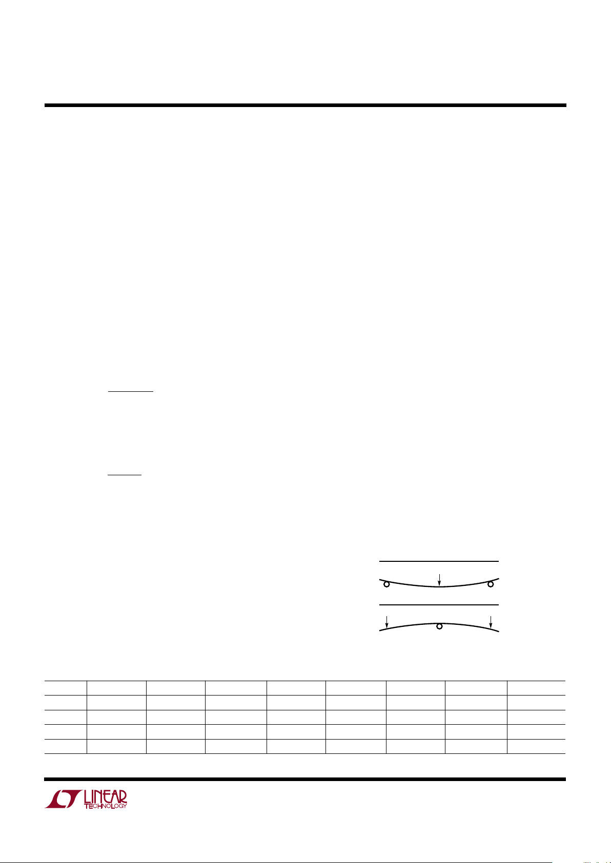
A qualitative technique to evaluate the effect of stress on
voltage references is to solder the part into a PC board and
deform the board a fixed amount as shown in Figure 6. The
flexure #1 represents no displacement, flexure #2 is
concave movement, flexure #3 is relaxation to no displacement and finally, flexure #4 is a convex movement.
This motion is repeated for a number of cycles and the
relative output deviation is noted. The result shown in
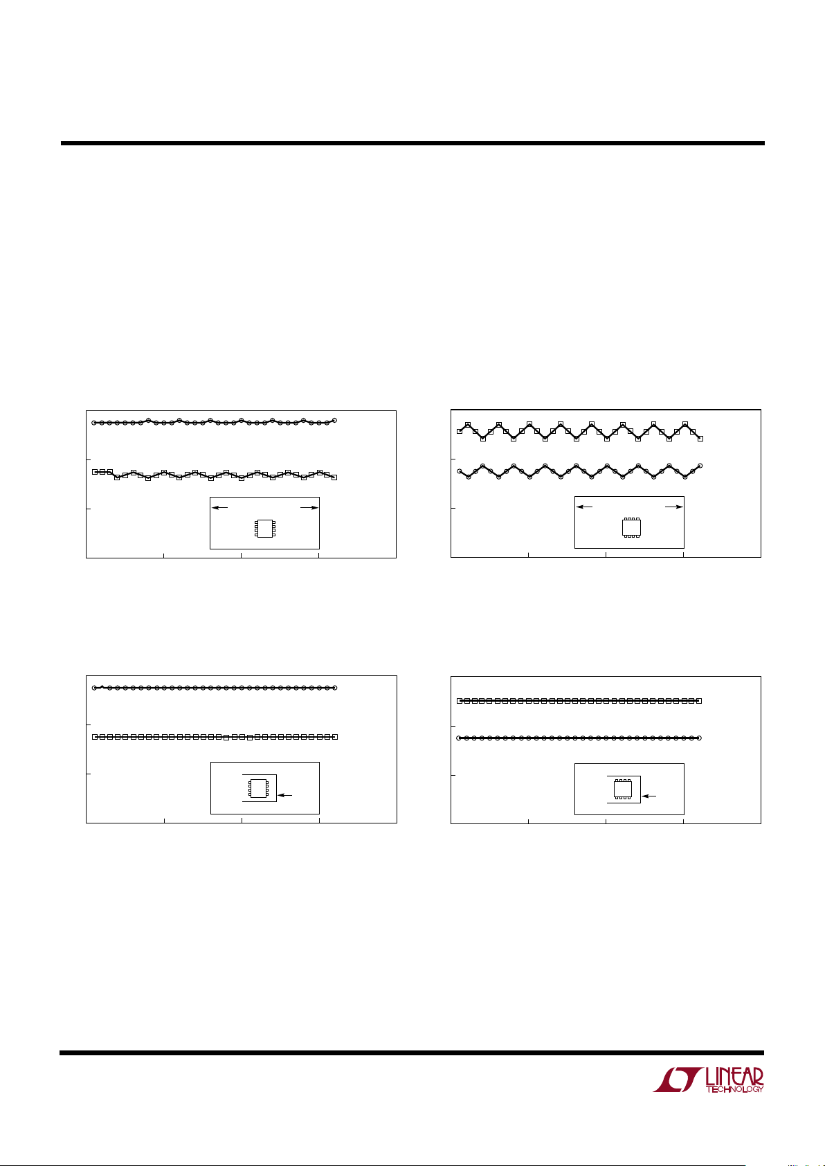
Figure 7a is for two LT1460S8-10s mounted vertically and
Figure 7b is for two LT1460S8-10s mounted horizontally.
The parts oriented in Figure 7a impart less stress into the
package because stress is absorbed in the leads. Figures
7a and 7b show the deviation to be between 500µV and
1
2
3
4
1460-10 F06
Output Accuracy
Like all references, either series or shunt, the error budget
of the LT1460-10 is made up of primarily three components: initial accuracy, temperature coefficient and load
regulation. Line regulation is neglected because it typically
contributes only 30ppm/V, or 300µV for a 1V input change.
The LT1460-10 typically shifts less than 0.01% when
soldered into a PCB, so this is also neglected (see PC
Board Layout section). The output errors are calculated as
follows for a 100µA load and 0° C to 70°C temperature
range:
LT1460AC
Initial accuracy = 0.075%
For IO = 100µA,
∆V
ppm
mA
mA V mV
OUT
=
()()
=
3500
01 10 35..
which is 0.035%.
For temperature 0°C to 70°C the maximum ∆T = 70°C,
∆V
ppm
C
CVmV
OUT
=
°
°
()()
=
10
70 10 7
which is 0.07%.
Total worst-case output error is:
0.075% + 0.035% + 0.070% = 0.180%.
Table 1 gives worst-case accuracy for the LT1460AC, CC,
DC, FC, GC from 0°C to 70°C and the LT1460BI, EI, GI
from –40°C to 85°C.
PC Board Layout
In 13- to 16-bit systems where initial accuracy and temperature coefficient calibrations have been done, the
mechanical and thermal stress on a PC board (in a cardcage
APPLICATIONS INFORMATION
WUU
U
Page 8
8
LT1460-10
Figure 7b. Two Typical LT1460S8-10s, Horizontal
Orientation Without Slots
SLOT
8
4
0
0
40
3020
FLEXURE NUMBER
10
1460-10 F08b
–4
OUTPUT DEVIATION (mV)
APPLICATIONS INFORMATION
WUU
U
1mV and implies a 50ppm and 100ppm change respectively. This corresponds to a 13- to 14-bit system and is
not a problem for most 10- to 12-bit systems unless the
system has a calibration. In this case, as with temperature
hysteresis, this low level can be important and even more
careful techniques are required.
The most effective technique to improve PC board stress
is to cut slots in the board around the reference to serve as
a strain relief. These slots can be cut on three sides of the
reference and the leads can exit on the fourth side. This
“tongue” of PC board material can be oriented in the long
direction of the board to further reduce stress transferred
to the reference.
The results of slotting the PC boards of Figures 7a and
7b are shown in Figures 8a and 8b. In this example the
slots can improve the output shift from about 100ppm to
nearly zero.
Figure 7a. Two Typical LT1460S8-10s, Vertical
Orientation Without Slots
LONG DIMENSION
8
4
0
0
40
3020
FLEXURE NUMBER
10
1460-10 F07a
–4
OUTPUT DEVIATION (mV)
SLOT
8
4
0
0
40
3020
FLEXURE NUMBER
10
1460-10 F08a
–4
OUTPUT DEVIATION (mV)
Figure 8a. Same Two LT1460S8-10s in Figure 7a,
but With Slots
FLEXURE NUMBER
1460-10 F07b
LONG DIMENSION
8
4
0
0
40
302010
–4
OUTPUT DEVIATION (mV)
Figure 8b. Same Two LT1460S8-10s in Figure 7b,
but With Slots
Page 9
9
LT1460-10
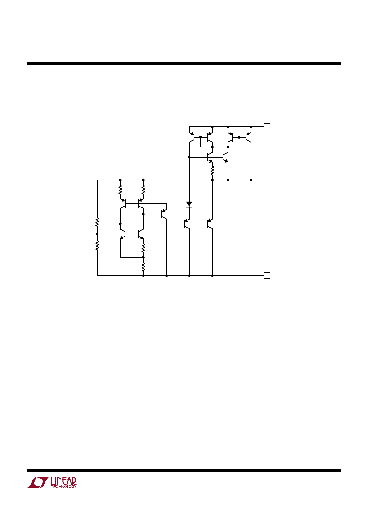
SI PLIFIED SCHE ATIC
WW
48k
360k
V
CC
V
OUT
GND
1460-5 SS
Page 10
10
LT1460-10
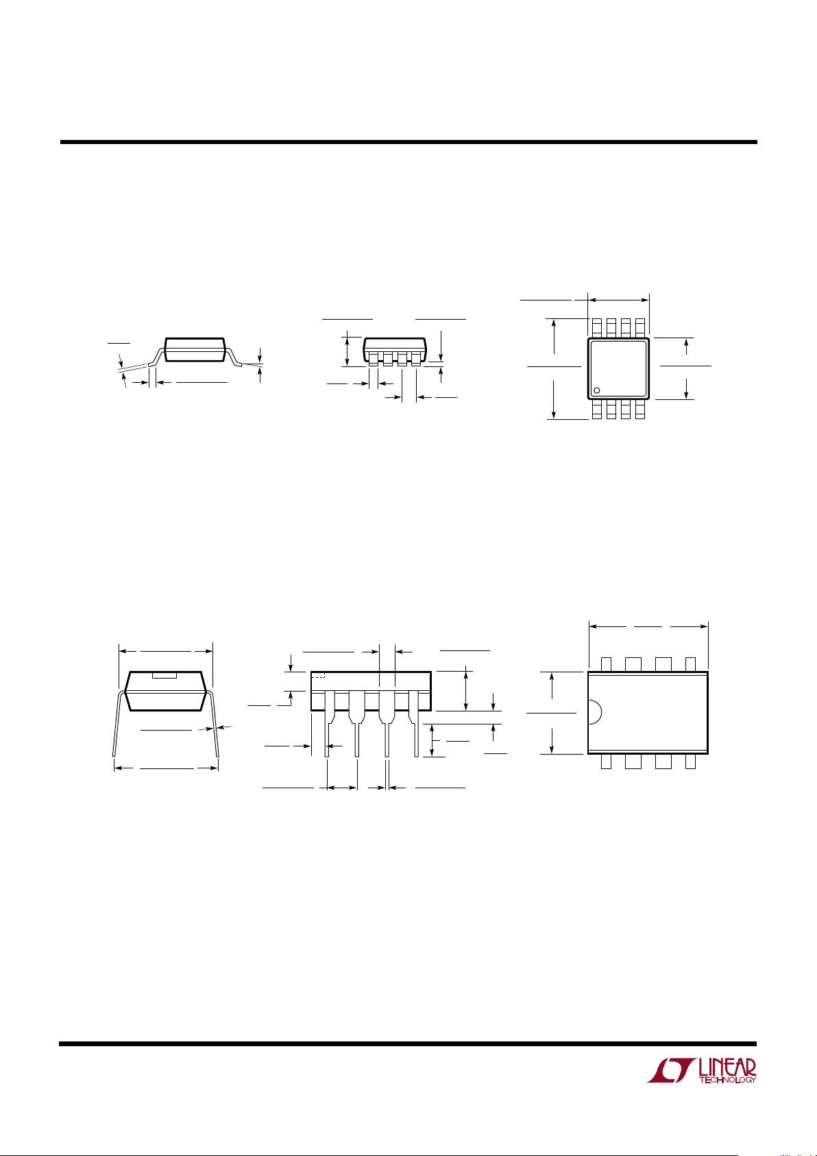
MS8 Package
8-Lead Plastic MSOP
(LTC DWG # 05-08-1660)
N8 Package
8-Lead PDIP (Narrow 0.300)
(LTC DWG # 05-08-1510)
Dimensions in inches (millimeters) unless otherwise noted.
PACKAGE DESCRIPTION
U
N8 0695
0.005
(0.127)
MIN
0.100 ± 0.010
(2.540 ± 0.254)
0.065
(1.651)
TYP
0.045 – 0.065
(1.143 – 1.651)
0.130 ± 0.005
(3.302 ± 0.127)
0.015
(0.380)
MIN
0.018 ± 0.003
(0.457 ± 0.076)
0.125
(3.175)
MIN
0.009 – 0.015
(0.229 – 0.381)
0.300 – 0.325
(7.620 – 8.255)
0.325
+0.025
–0.015
+0.635
–0.381
8.255
()
12
3
4
876
5
0.255 ± 0.015*
(6.477 ± 0.381)
0.400*
(10.160)
MAX
*THESE DIMENSIONS DO NOT INCLUDE MOLD FLASH OR PROTRUSIONS.
MOLD FLASH OR PROTRUSIONS SHALL NOT EXCEED 0.010 INCH (0.254mm)
MSOP08 0595
* DIMENSION DOES NOT INCLUDE MOLD FLASH, PROTRUSIONS OR GATE BURRS. MOLD FLASH,
PROTRUSIONS OR GATE BURRS SHALL NOT EXCEED 0.006" (0.152mm) PER SIDE
** DIMENSION DOES NOT INCLUDE INTERLEAD FLASH OR PROTRUSIONS.
INTERLEAD FLASH OR PROTRUSIONS SHALL NOT EXCEED 0.006" (0.152mm) PER SIDE
0.021 ± 0.004
(0.53 ± 0.01)
0° – 6° TYP
0.007
(0.18)
0.040 ± 0.006
(1.02 ± 0.15)
0.012
(0.30)
0.006 ± 0.004
(0.15 ± 0.10)
0.025
(0.65)
TYP
12
3
4
0.192 ± 0.004
(4.88 ± 0.10)
8
7
6
5
0.118 ± 0.004*
(3.00 ± 0.10)
0.118 ± 0.004**
(3.00 ± 0.10)
Page 11
11
LT1460-10
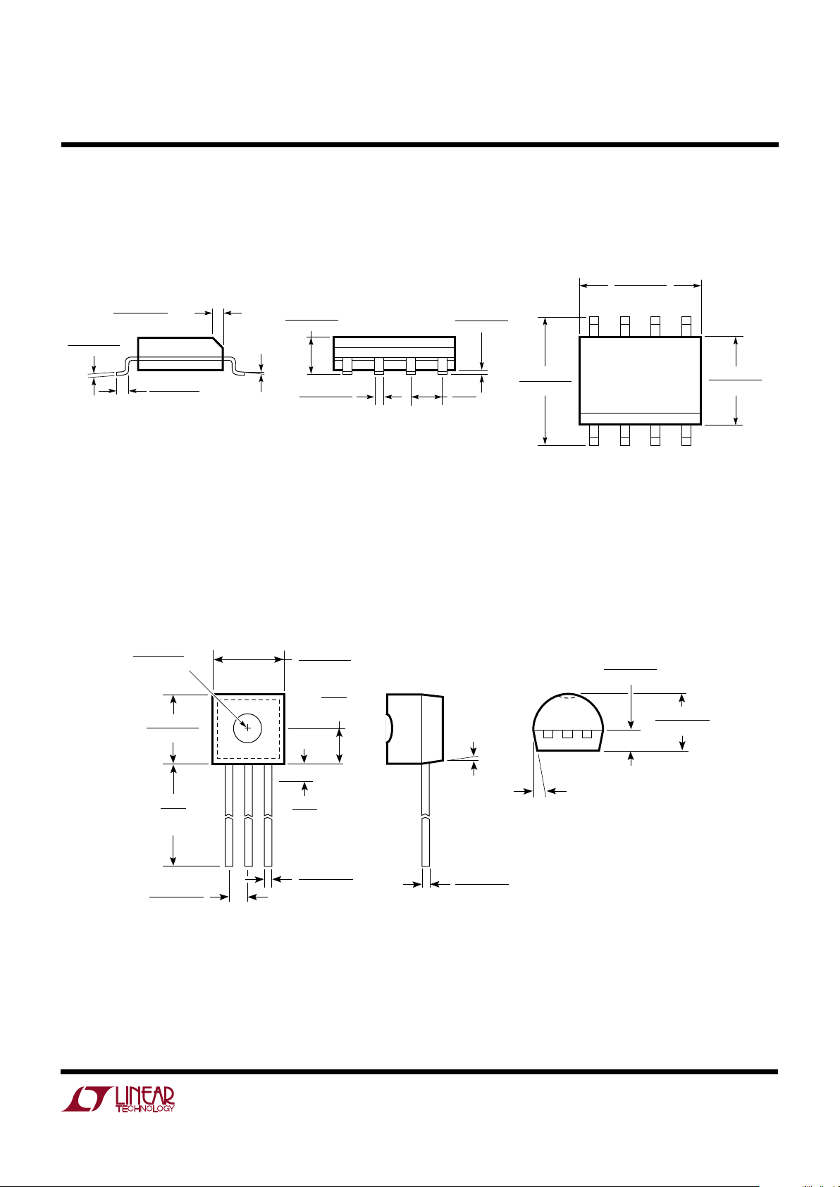
Dimensions in inches (millimeters) unless otherwise noted.
PACKAGE DESCRIPTION
U
S8 Package
8-Lead Plastic Small Outline (Narrow 0.150)
(LTC DWG # 05-08-1610)
Z Package
3-Lead Plastic TO-92 (Similar to TO-226)
(LTC DWG # 05-08-1410)
0.016 – 0.050
0.406 – 1.270
0.010 – 0.020
(0.254 – 0.508)
× 45°
0°– 8° TYP
0.008 – 0.010
(0.203 – 0.254)
SO8 0695
0.053 – 0.069
(1.346 – 1.752)
0.014 – 0.019
(0.355 – 0.483)
0.004 – 0.010
(0.101 – 0.254)
0.050
(1.270)
BSC
1
2
3
4
0.150 – 0.157**
(3.810 – 3.988)
8
7
6
5
0.189 – 0.197*
(4.801 – 5.004)
0.228 – 0.244
(5.791 – 6.197)
DIMENSION DOES NOT INCLUDE MOLD FLASH. MOLD FLASH
SHALL NOT EXCEED 0.006" (0.152mm) PER SIDE
DIMENSION DOES NOT INCLUDE INTERLEAD FLASH. INTERLEAD
FLASH SHALL NOT EXCEED 0.010" (0.254mm) PER SIDE
*
**
0.050 ± 0.005
(1.270 ± 0.127)
0.060 ± 0.005
(1.524± 0.127)
DIA
0.90
(2.286)
NOM
0.180 ± 0.005
(4.572 ± 0.127)
0.180 ± 0.005
(4.572 ± 0.127)
0.500
(12.70)
MIN
0.050
(1.270)
MAX
UNCONTROLLED
LEAD DIMENSION
0.016 ± 0.003
(0.406 ± 0.076)
5°
NOM
0.015 ± 0.002
(0.381 ± 0.051)
0.060 ± 0.010
(1.524 ± 0.254)
10° NOM
0.140 ± 0.010
(3.556 ± 0.127)
Z3 (TO-92) 0695
Information furnished by Linear Technology Corporation is believed to be accurate and reliable.
However, no responsibility is assumed for its use. Linear Technology Corporation makes no representation that the interconnection of its circuits as described herein will not infringe on existing patent rights.
Page 12
12
LT1460-10
146010f LT/TP 1097 4K • PRINTED IN USA
LINEAR TECHNOLOGY CORPORATION 1997
Linear Technology Corporation
1630 McCarthy Blvd., Milpitas, CA 95035-7417 ● (408) 432-1900
FAX: (408) 434-0507
●
TELEX: 499-3977 ● www.linear-tech.com
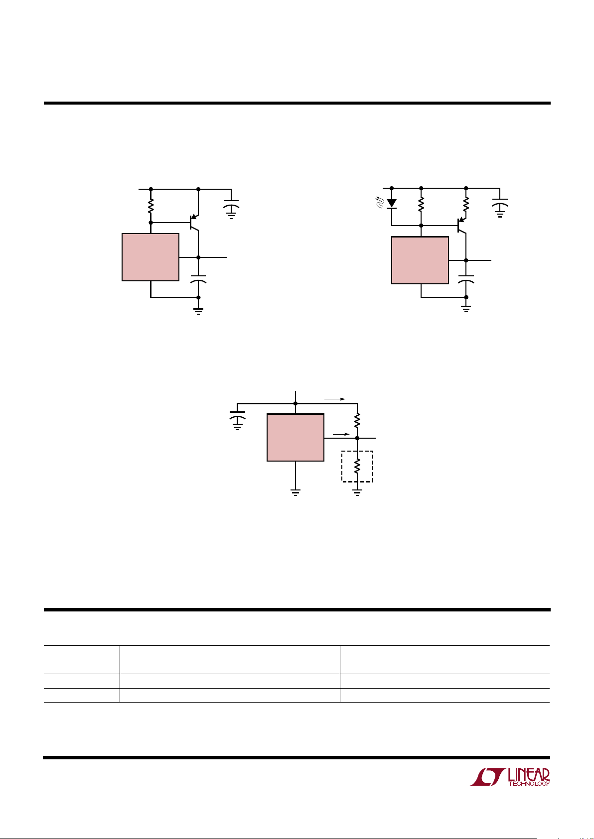
Boosted Output Current with No Current Limit Boosted Output Current with Current Limit
V+ ≥ (V
OUT
+ 1.8V)
LT1460-10
OUT
GND
IN
1460-10 TA03
2N2905
10V
100mA
47µF
2µF
SOLID
TANT
R1
220Ω
+
+
TYPICAL APPLICATIONS
U
1460-10 TA04
2N2905
10V
100mA
2µF
SOLID
TANT
D1*
LED
V+ ≥ V
OUT
+ 2.8V
8.2Ω
R1
220Ω
GLOWS IN CURRENT LIMIT,
DO NOT OMIT
*
47µF
+
+
LT1460-10
OUT
GND
IN
RELATED PARTS
PART NUMBER DESCRIPTION COMMENTS
LT1019 Precision Bandgap Reference 0.05% Max, 5ppm/°C Max
LT1236 Precision Low Noise Reference 0.05% Max, 5ppm/°C Max, SO Package
LT1634 Micropower Precision Shunt Reference 0.05%, Max, 25ppm/°C Max
Handling Higher Load Currents
1460-10 TA05
R
L
40mA
12.5V
R1*
63Ω
V
OUT
10V
TYPICAL LOAD
CURRENT = 50mA
SELECT R1 TO DELIVER 80% OF TYPICAL LOAD CURRENT.
LT1460 WILL THEN SOURCE AS NECESSARY TO MAINTAIN
PROPER OUTPUT. DO NOT REMOVE LOAD AS OUTPUT WILL
BE DRIVEN UNREGULATED HIGH. LINE REGULATION IS
DEGRADED IN THIS APPLICATION
*
10mA
47µF
+
LT1460-10
OUT
GND
IN
 Loading...