

Page 1
FEATURES
■
Handles 10,000pF Capacitive Load
■
450µV Max Offset Voltage
■
1200µV Max Offset Voltage in S8 Package
■
50pA Bias Current at 70°C
■
13nV/√Hz Voltage Noise
■
4V/µs Slew Rate
■
4µV/°C Drift
■
130dB Channel Separation
U
APPLICATIONS
■
Sample-and-Hold (Drives Large Hold Capacitors)
■
A/D and D/A Converters
■
Photodiode Amplifiers
■
Voltage-to-Frequency Converters
LT1457
Dual, Precision
JFET Input Op Amp
U
DESCRIPTION
The LT1457 is a dual, JFET input op amp optimized for
handling large capacitive loads in combination with precision performance.
Precision specifications include 220µV offset voltage in
plastic and surface mount packages. At 70°C input bias
current is 50pA, input offset current is 20pA. Channel
separation is 130dB.
Other dual JFET input op amps from Linear Technology
include the LT1057, which is three times faster than the
LT1457 but at the expense of significantly lower capacitive
load handling capability; and the LT1113 with 4.5nV/√Hz
voltage noise.
UW
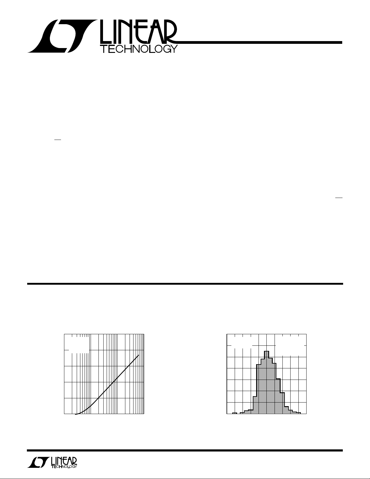
TYPICAL PERFORMANCE CHARACTERISTICS
Capacitive Load Handling
100
VS = ±15V
= 25°C
T
A
= +1
A
80
V
60
40
OVERSHOOT (%)
20
0
0.1 1 10
CAPACITIVE LOAD (nF)
100
LT11457• TA01
PERCENT OF UNITS
Input Offset Voltage Distribution
S8 Package
21
VS = ±15V
T
= 25°C
18
A
15
12
9
6
3
0
–1.0 –0.6 –0.2 0.60.2–0.8 –0.4 0 0.80.4
INPUT OFFSET VOLTAGE (mV)
400 DUALS
(800 OP AMPS)
TESTED FROM
3 RUNS
1.0
LT1457 • TA02
1
Page 2
LT1457
WW
W
U
ABSOLUTE MAXIMUM RATINGS
Supply Voltage ...................................................... ±20V
Differential Input Voltage .......................................±40V
Input Voltage .......................... Equal to Supply Voltages
Output Short-Circuit Duration.......................... Indefinite
Operating Temperature Range ................ –40°C to 85°C
Storage Temperature Range ................. – 65°C to 150°C
Lead Temperature (Soldering, 10 sec).................. 300°C
U
W
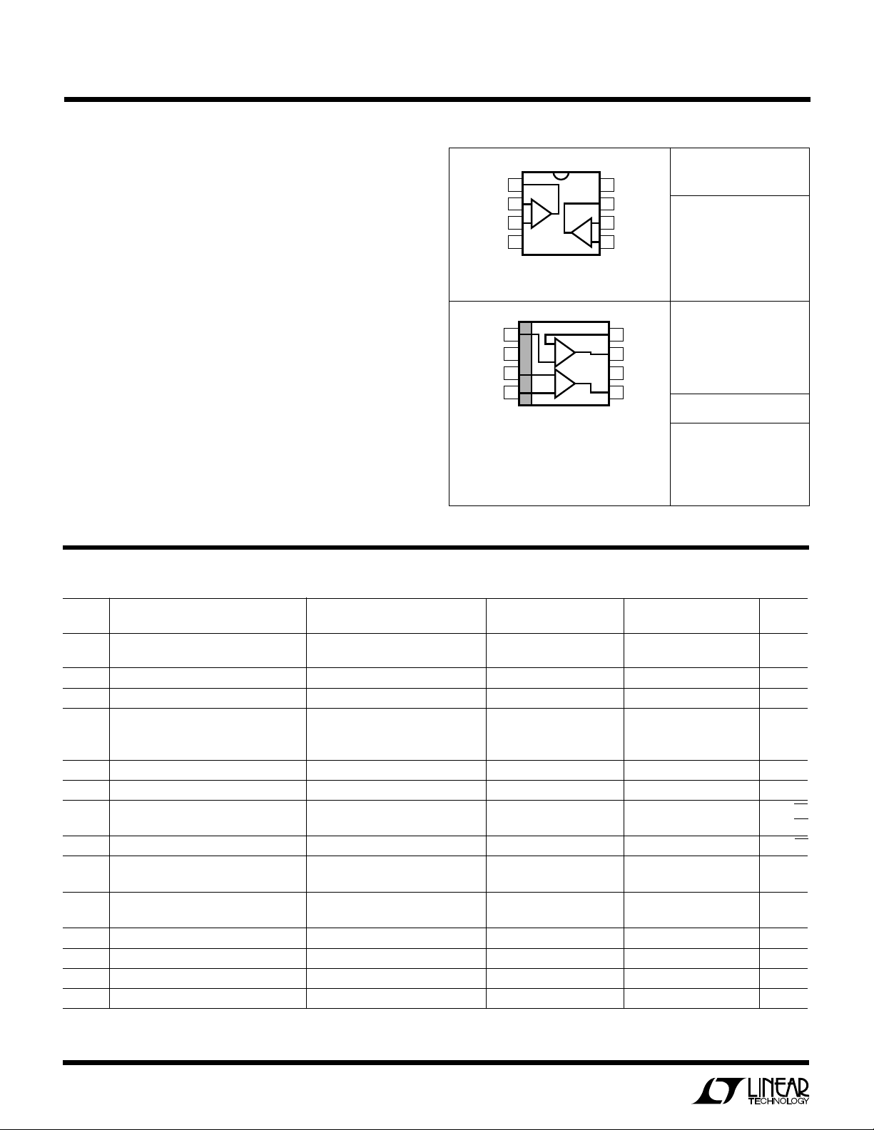
PACKAGE/ORDER INFORMATION
TOP VIEW
+
1
OUT A
2
–IN A
+IN A
V
+IN A
V
+IN B
–IN B
NOTE: THIS PIN CONFIGURATION DIFFERS FROM
THE 8-LEAD DIP PIN LOCATIONS. INSTEAD, IT
FOLLOWS THE INDUSTRY STANDARD LT1013DS8
SO PACKAGE CONFIGURATION.
Consult factory for Industrial and Military grade parts.
A
3
–
N8 PACKAGE
8-LEAD PLASTIC DIP
T
= 115°C, θJA = 130°C/W
JMAX
TOP VIEW
1
–
2
3
4
S8 PACKAGE
8-LEAD PLASTIC SOIC
T
= 130°C, θJA = 190°C/ W
JMAX
A
B
8
V
7
OUT B
6
–IN B
B
+IN B
54
–IN A
8
7
OUT A
+
6
V
OUT B
5
ORDER PART
NUMBER
LT1457ACN8
LT1457CN8
LT1457S8
S8 PART MARKING
1457
U
ELECTRICAL CHARACTERISTICS
SYMBOL PARAMETER CONDITIONS MIN TYP MAX MIN TYP MAX UNITS
V
OS
I
OS
I
B
e
n
e
n
i
n
A
VOL
CMRR Common-Mode Rejection Ratio VCM = ±10.5V 86 100 82 98 dB
PSRR Power Supply Rejection Ratio VS = ±4.5V to ±18V 88 103 86 102 dB
V
OUT
SR Slew Rate 2 4 2 4 V/µs
Input Offset Voltage LT1457AC/C 150 450 200 800 µV
LT1457S8 220 1200 µV
Input Offset Current Fully Warmed Up 3 40 4 50 pA
Input Bias Current Fully Warmed Up ±5 ±50 ±7 ±75 pA
Input Resistance-Differential 10
-Common-Mode V
Input Capacitance 4 4 pF
Input Noise Voltage 0.1Hz to 10Hz 2.0 2.1 µV
Input Noise Voltage Density fO = 10Hz 26 28 nV/√Hz
Input Noise Current Density fO = 10Hz, 1kHz (Note 3) 1.5 4 1.8 6 fA/√Hz
Large-Signal Voltage Gain VO = ±10V, RL = 2k 150 350 100 300 V/mV
Input Voltage Range ±10.5 14.3 ±10.5 14.3 V
Output Voltage Swing RL = 2k ±12 ±13 ±12 ±13 V
= –11V to 8V 10
CM
VCM = 8V to 11V 10
= 1kHz (Note 2) 13 22 14 24 nV/√Hz
f
O
= ±10V, RL = 1k 120 250 80 220 V/mV
V
O
VS = ±15V, TA = 25°C,VCM = 0V unless otherwise noted. (Note 1)
LT1457AC LT1457C/LT1457S8
12
12
11
–11.5 –11.5 V
10
10
10
12
12
11
P–P
Ω
Ω
Ω
2
Page 3
LT1457
ELECTRICAL CHARACTERISTICS
SYMBOL PARAMETER CONDITIONS MIN TYP MAX MIN TYP MAX UNITS
GBW Gain-Bandwidth Product (Note 5) 1.0 1.7 1.0 1.7 MHz
I
S
Supply Current Per Amplifier 1.8 3.0 1.8 3.0 mA
Channel Separation DC to 5kHz, VIN = ±10V 132 130 dB
ELECTRICAL CHARACTERISTICS
SYMBOL PARAMETER CONDITIONS MIN TYP MAX MIN TYP MAX UNITS
V
OS
I
OS
I
B
A
VOL
CMRR Common-Mode Rejection Ratio VCM = ±10.4V ● 85 98 80 96 dB
PSRR Power Supply Rejection Ratio VS = ±4.5V to ±18V ● 87 102 84 100 dB
V
OUT
I
S
Input Offset Voltage LT1457AC/C ● 250 900 330 1500 µV
LT1457S8 ● 400 1900 µV
Average Temperature Coefficient of ● 310 416 µV/°C
Input Offset Voltage (Note 4)
Input Offset Current Warmed Up, TA = 70°C 18 150 20 250 pA
Input Bias Current Warmed Up, TA = 70°C ±50 ±250 ±60 ±350 pA
Large-Signal Voltage Gain VO = ±10V, RL = 2k ● 70 220 50 200 V/mV
Output Voltage Swing RL = 2k ● ±12 ±12.8 ±12 ±12.8 V
Supply Current Per Amplifier ● 3.2 3.2 mA
TA = 70°C 1.7 1.7 mA
VS = ±15V, TA = 25°C,VCM = 0V unless otherwise noted. (Note 1)
LT1457AC LT1457C/LT1457S8
VS = ±15V, VCM = 0V, 0°C ≤ TA ≤ 70°C, unless otherwise noted.
LT1457AC LT1457C/LT1457S8
ELECTRICAL CHARACTERISTICS
SYMBOL PARAMETER CONDITIONS MIN TYP MAX MIN TYP MAX UNITS
V
OS
I
OS
I
B
A
VOL
CMRR Common-Mode Rejection Ratio VCM = ±10.4V ● 84 97 80 95 dB
PSRR Power Supply Rejection Ratio VS = ±5V to ±17V ● 86 100 83 98 dB
V
OUT
I
S
The ● denotes the specifications which apply over the full operating
temperature range.
Note 1: Typical parameters are defined as the 60% yield of distributions of
individual amplifiers; i.e., out of 100 LT1457s (200 op amps) typically 120
will be better than the indicated specification.
Note 2: This parameter is tested on a sample basis only.
Note 3: Current noise is calculated from the formula: i
q = 1.6 x 10
swamps the contribution of current noise.
Input Offset Voltage LT1457AC/C ● 350 1100 400 1800 µV
LT1457S8 ● 500 2300 µV
Average Temperature Coefficient of ● 310 416 µV/°C
Input Offset Voltage
Input Offset Current Warmed Up, TA = 85°C 0.1 0.5 0.1 0.6 nA
Input Bias Current Warmed Up, TA = 85°C ±0.2 ±0.7 ±0.2 ±0.9 nA
Large-Signal Voltage Gain VO = ±10V, RL = 2k ● 40 120 30 110 V/mV
Output Voltage Swing RL = 2k ● ±12 ±12.7 ±12 ±12.6 V
Supply Current Per Amplifier TA = – 40°C 3.8 3.8 mA
TA = 85°C 1.7 1.7 mA
= (2qIb)
–19
coulomb. The noise of source resistors up to 1GΩ
n
VS = ±15V, VCM = 0V, –40°C ≤ TA ≤ 85°C, unless otherwise noted. (Note 6)
LT1457AC LT1457C/LT1457S8
Note 4: This parameter is not 100% tested.
Note 5: Gain-Bandwidth product is not tested. It is guaranteed by design
and by inference from the slew rate measurement.
Note 6: The LT1457 is not tested and not quality-assurance-sampled at
–40°C and at 85°C. These specifications are guaranteed by design,
correlation, and/or inference from 0°C, 25°C, and 70°C tests.
1/2
, where
3
Page 4

LT1457
VS = ±15V
T
A
= 25°C
N8 PACKAGE
S8 PACKAGE
TIME AFTER POWER ON (MINUTES)
0
60
30
120
90
150
CHANGE IN OFFSET VOLTAGE (µV)
5
LT1457 • TPC03
01234
VS = ±15V
T
A
= 25°C
TIME (MONTHS)
–50
–30
–10
10
30
50
OFFSET VOLTAGE CHANGE (µV)
5
–40
–20
0
20
40
LT1457 • TPC06
012 43
FREQUENCY (Hz)
60
100
80
140
120
160
CHANNEL SEPARATION (dB)
1M
LT1457 • TPC09
1 10 100 1k 10k 100k
VS = ±15V
T
A
= 25°C
V
IN
= 20V
P-P
TO 5kHz
R
L
= 2k
LIMITED BY
THERMAL
INTERACTION AT
DC = 132dB
LIMITED BY PIN TO
PIN CAPACITANCE
RS = 10Ω
RS = 1k
W
U
TYPICAL PERFORMANCE CHARACTERISTICS
Input Bias and Offset Current vs
Temperature
1000
VS = ±15V
= 0V
V
CM
WARMED UP
300
100
BIAS CURRENT
30
10
INPUT BIAS AND OFFSET CURRENT (pA)
3
0255075
AMBIENT TEMPERATURE (°C)
OFFSET CURRENT
Input Offset Voltage Distribution
N8 Package
24
VS = ±15V
= 25°C
T
21
A
18
15
12
9
PERCENT OF UNITS
6
3
0
–0.6
–0.8
–0.4
INPUT OFFSET VOLTAGE (mV)
–0.2
900 DUALS
(1800 OP AMPS)
TESTED FROM 3
RUNS
0
0.2
LT1457 • TPC01
0.4
LT1457 • TPC04
0.6
100
0.8
Input Bias Current Over
the Common-Mode Range
160
VS = ±15V
140
120
100
80
60
40
INPUT BIAS CURRENT (pA)
20
0
–20
–15 –10 –5 0 5 10
COMMON-MODE INPUT VOLTAGE (V)
1000
300
100
VOLTAGE GAIN (V/mV)
30
10
–50 25–25 500
TA = 70°C
RL = 2k
RL = 1k
TEMPERATURE (°C)
TA = 25°C
LT1457 • TPC02
VS = ±15V
= ±10V
V
O
LT1457 • TPC05
Warm-Up Drift
15
Long Term Drift of
Representative UnitsVoltage Gain vs Temperature
10075
100
VS = ±15V
= 25°C
T
A
70
50
30
20
RMS VOLTAGE NOISE DENSITY (nV/√Hz)
10
3 10 30 100 300 1k 3k
4
1/f CORNER = 28Hz
FREQUENCY (Hz)
LT1457 • TPC07
10k
0.1Hz to 10Hz NoiseVoltage Noise vs Frequency Channel Separation vs Frequency
VS = ±15V
= 25°C
T
A
NOISE VOLTAGE (1µV/DIV)
024 86
TIME (SECONDS)
10
LT1457 • TPC08
Page 5

W
TEMPERATURE (°C)
90
100
110
120
CMRR, PSRR (dB)
100
LT1457 • TPC12
–50 –25 0 7525 50
VS = ±5V TO ±17V FOR PSRR
V
S
= ±15V, VCM = ±10.5V FOR CMRR
PSRR
CMRR
TIME FROM OUTPUT SHORT TO GROUND (MINUTES)
–50
–30
–10
10
30
–40
–20
0
20
40
50
SHORT-CIRCUIT CURRENT (mA)
LT1457 • TPC15
01 32
V
S
= ±15V
TA = –40°C
TA = 85°C
TA = 25°C
TA = 85°C
TA = –40°C
TA = 25°C
FREQUENCY (Hz)
0
40
20
60
80
120
100
140
PSRR (dB)
10M
LT1457• TPC13
10 100 1k 10k 1M100k
TA = 25°C
POSITIVE
SUPPLY
NEGATIVE
SUPPLY
U
TYPICAL PERFORMANCE CHARACTERISTICS
LT1457
Common-Mode Rejection Ratio
vs Frequency
120
100
80
60
CMRR (dB)
40
20
0
10 100 1k 10k 1M100k
FREQUENCY (Hz)
Slew Rate, Gain-Bandwidth
Product vs Temperature
10
8
6
4
SLEW RATE (V/µs)
2
–50–250 255075
TEMPERATURE (°C)
VS = ±15V
VS = ±15V
= 25°C
T
A
LT1457• TPC10
SLEW FALL
GBW
SLEW RISE
LT1457 • TPC18
10M
100
2.5
2.0
1.5
1.0
Common-Mode Range vs
Temperature
15
14
13
12
11
±10
–11
–12
COMMON -MODE RANGE (V)
–13
–14
VS = ±15V
–15
–50 –25 0 25 7550
3
GBW (MHz)
2
1
SUPPLY CURRENT PER AMPLIFIER (mA)
0
–50 –25 0 7525 50
TEMPERATURE (°C)
VS = ±5V
TEMPERATURE (°C)
VS = ±15V
Common-Mode and Power Supply
Rejections vs Temperature
100
LT1457 • TPC11
Short-Circuit Current vs Time
(One Output Shorted to Ground)Supply Current vs Temperature
100
LT1457 • TPC14
Gain, Phase vs Frequency
25
20
15
10
5
0
VOLTAGE GAIN (dB)
–5
–10
–15
PHASE MARGIN = 80°, CL = 10pF
PHASE MARGIN = 51°, C
GAIN
VS = ±15V
= 25°C
T
A
0.1 1.0
CL = 1000pF
CL = 10pF
FREQUENCY (MHz)
= 1000pF
L
CL = 10pF
PHASE
CL = 1000pF
LT1457 • TPC16
100
PHASE MARGIN (DEG)
80
60
40
20
0
–20
10
Undistorted Output Swing vs
Frequency
30
24
18
12
6
PEAK TO PEAK OUTPUT SWING (V)
0
10k 100k 1M
FREQUENCY (Hz)
VS = ±15V
T
= 25°C
A
LT11457• TPC17
Power Supply Rejection Ratio
vs Frequency
10M
5
Page 6

LT1457
W
U
TYPICAL PERFORMANCE CHARACTERISTICS
Large-Signal Response
AV = 1, CL = 100pF
U
WUU
Small-Signal Response
AV = 1, CL = 1000pF
APPLICATIONS INFORMATION
Phase Reversal Protection
Most industry standard JFET input single, dual, and quad
op amps (e.g., LF156, LF351, LF353, LF411, LF412,
OP-15, OP-16, OP-215, and TL084) exhibit phase reversal
at the output when the negative common-mode limit at the
input is exceeded (i.e., below –12V with ±15V supplies).
The photos show a ±16V sine wave input (A), the response
Small-Signal Response
AV = 1, CL = 10,000pF
LT1457 TPC20LT1457 TPC19 LT1457 TPC21
of an LF412A in the unity gain follower mode (B), and the
response of the LT1457 (C).
The phase reversal of photo (B) can cause lock-up in servo
systems. The LT1457 does not phase-reverse due to a
unique phase reversal protection circuit.
6
LT1457 AI03LT1457 AI01 LT1457 AI02
(B) LF412A Output(A) ±16V Sine Wave Input (C) LT1457 Output
All Photos 5V/Div Vertical Scale, 50µs/Div Horizontal Scale
Page 7

LT1457
U
WUU
APPLICATIONS INFORMATION
High Speed Operation
When the feedback around the op amp is resisitive (RF), a
pole will be created with RF, the source resistance and
capacitance (RS, CS), and the amplifier input capacitance
(CIN ≈ 4pF). In low closed loop gain configurations and
with RS and RF in the kilohm range, this pole can create
excess phase shift and even oscillation on high speed
amplifiers. Because the LT1457’s phase margin is very
high, this problem is minimal. However, a small capacitor
(CF) in parallel with RF eliminates this problem. With RS(C
S
+ CIN) = RFCF, the effect of the feedback pole is completely
removed.
U
PACKAGE DESCRIPTION
Dimension in inches (millimeters) unless otherwise noted.
N8 Package
8-Lead Plastic DIP
C
F
R
F
–
C
C
R
S
S
IN
+
OUTPUT
LT1457 AI04
0°– 8° TYP
0.300 – 0.320
(7.620 – 8.128)
0.065
(1.651)
0.009 – 0.015
(0.229 – 0.381)
+0.025
0.325
–0.015
+0.635
8.255
()
–0.381
TYP
0.045 ± 0.015
(1.143 ± 0.381)
(2.540 ± 0.254)
0.045 – 0.065
(1.143 – 1.651)
0.100 ± 0.010
S8 Package
8-Lead Plastic SOIC
0.010 – 0.020
(0.254 – 0.508)
0.016 – 0.050
0.406 – 1.270
× 45°
0.008 – 0.010
(0.203 – 0.254)
0.053 – 0.069
(1.346 – 1.752)
0.014 – 0.019
(0.355 – 0.483)
0.130 ± 0.005
(3.302 ± 0.127)
0.125
(3.175)
MIN
0.018 ± 0.003
(0.457 ± 0.076)
0.004 – 0.010
(0.101 – 0.254)
0.050
(1.270)
BSC
0.020
(0.508)
MIN
0.228 – 0.244
(5.791 – 6.197)
0.400
(10.160)
MAX
876
12
0.189 – 0.197
(4.801 – 5.004)
8
3
7
5
4
6
0.250 ± 0.010
(6.350 ± 0.254)
5
0.150 – 0.157
(3.810 – 3.988)
N8 0392
1
Information furnished by Linear Technology Corporation is believed to be accurate and reliable.
However, no responsibility is assumed for its use. Linear Technology Corporation makes no representation that the interconnection of its circuits as described herein will not infringe on existing patent rights.
3
2
4
SO8 0392
7
Page 8

LT1457
U.S. Area Sales Offices
NORTHEAST REGION
Linear Technology Corporation
One Oxford Valley
2300 E. Lincoln Hwy.,Suite 306
Langhorne, PA 19047
Phone: (215) 757-8578
FAX: (215) 757-5631
Linear Technology Corporation
266 Lowell St., Suite B-8
Wilmington, MA 01887
Phone: (508) 658-3881
FAX: (508) 658-2701
FRANCE
Linear Technology S.A.R.L.
Immeuble "Le Quartz"
58 Chemin de la Justice
92290 Chatenay Malabry
France
Phone: 33-1-41079555
FAX: 33-1-46314613
SOUTHEAST REGION
Linear Technology Corporation
17060 Dallas Parkway
Suite 208
Dallas, TX 75248
Phone: (214) 733-3071
FAX: (214) 380-5138
CENTRAL REGION
Linear Technology Corporation
Chesapeake Square
229 Mitchell Court, Suite A-25
Addison, IL 60101
Phone: (708) 620-6910
FAX: (708) 620-6977
International Sales Offices
KOREA
Linear Technology Korea Branch
Namsong Building, #505
Itaewon-Dong 260-199
Yongsan-Ku, Seoul
Korea
Phone: 82-2-792-1617
FAX: 82-2-792-1619
SOUTHWEST REGION
Linear Technology Corporation
22141 Ventura Blvd.
Suite 206
Woodland Hills, CA 91364
Phone: (818) 703-0835
FAX: (818) 703-0517
NORTHWEST REGION
Linear Technology Corporation
782 Sycamore Dr.
Milpitas, CA 95035
Phone: (408) 428-2050
FAX: (408) 432-6331
TAIWAN
Linear Technology Corporation
Rm. 801, No. 46, Sec. 2
Chung Shan N. Rd.
Taipei, Taiwan, R.O.C.
Phone: 886-2-521-7575
FAX: 886-2-562-2285
GERMANY
Linear Techonolgy GmbH
Untere Hauptstr. 9
D-85386 Eching
Germany
Phone: 49-89-3197410
FAX: 49-89-3194821
JAPAN
Linear Technology KK
5F YZ Bldg.
4-4-12 Iidabashi, Chiyoda-Ku
Tokyo, 102 Japan
Phone: 81-3-3237-7891
FAX: 81-3-3237-8010
SINGAPORE
Linear Technology Pte. Ltd.
101 Boon Keng Road
#02-15 Kallang Ind. Estates
Singapore 1233
Phone: 65-293-5322
FAX: 65-292-0398
World Headquarters
Linear Technology Corporation
1630 McCarthy Blvd.
Milpitas, CA 95035-7487
Phone: (408) 432-1900
FAX: (408) 434-0507
UNITED KINGDOM
Linear Technology (UK) Ltd.
The Coliseum, Riverside Way
Camberley, Surrey GU15 3YL
United Kingdom
Phone: 44-276-677676
FAX: 44-276-64851
0294
8
Linear Technology Corporation
1630 McCarthy Blvd., Milpitas, CA 95035-7487
(408) 432-1900
●
FAX
: (408) 434-0507
●
TELEX
: 499-3977
LT/GP 0594 10K • PRINTED IN USA
LINEAR TECHNOLOGY CORPORATION 1994
 Loading...