

Page 1
LT1432-3.3
3.3V High Efficiency Step-Down
Switching Regulator Controller
EATU
F
■
Accurate Preset 3.3V Output
■
Up to 87% Efficiency
■
Optional Burst ModeTM Operation for Light Loads
■
Can Be Used with Many LTC Switching ICs
■
Accurate Ultra-Low-Loss Current Limit
■
Operates with Inputs from 4.5V to 30V
■
Shutdown Mode Draws Only 15µA
■
Uses Small 30µH Inductor
PPLICATI
A
■
Laptop and Palmtop Computers
■
Portable Data-Gathering Instruments
, LTC and LT are registered trademarks of Linear Technology Corporation.
Burst Mode is a trademark of Linear Technology Corporation.
RE
S
O
U
S
DUESCRIPTIO
The LT®1432-3.3 is a control chip designed to operate
with the LT1171/LT1271 family of switching regulators to
make a very high efficiency 3.3V step-down (buck) switching regulator. A minimum of external components is
needed.
Included is an accurate current limit which uses only
60mV sense voltage and uses “free” PC board trace
material for the sense resistor. Logic controlled electronic
shutdown mode draws only 15µA battery current. The
switching regulator operates down to 4.5V input.
The LT1432-3.3 has a logic controlled Burst Mode operation
to achieve high efficiency at very light load currents (0mA to
100mA) such as memory keep-alive. In normal switching
mode, the standby power loss is about 30mW, limiting
efficiency at light loads. In Burst Mode operation, standby
loss is reduced to approximately 11mW. Output current in
this mode is typically in the 5mA to 100mA range.
The LT1432-3.3 is available in 8-pin SO and PDIP packages. The LT1171/LT1271 is also available in surface
mount DD packages.
V
IN
+
C1
330µF
35V
MODE LOGIC
<0.3V = NORMAL MODE
>2.5V = SHUTDOWN
OPEN = Burst Mode
OPERATION
U
O
A
PPLICATITYPICAL
D2
1N5818
V
SW
LT1271
FB
V
C
C6
0.02µF
D1
MBR330p
V
MODE
220pF
†
FOR CIRCUITS WHICH DO NOT USE
Burst Mode OPERATION, C5 MAY
BE PARALLEL WITH A 680Ω, 0.1µF
IN SERIES TO GIVE WIDE PHASE MARGIN
WITH DIFFERENT SWITCHING ICs AND
OUTPUT CAPACITORS
V
IN
GND
C3
10µF
TANT
DIODE
LT1432-3.3
GND
+
†
C5
0.03µF
V
C
IN
D2**
L1
R2*
30µH
0.013Ω
+
V
V
LIM
V
OUT
*R2 IS MADE FROM PC BOARD
COPPER TRACES.
**OPTIONAL CONNECTION FOR D2.
EFFICIENCY IS HIGHER, BUT MINIMUM
INCREASES. SEE APPLICATION
V
IN
INFORMATION SECTION.
***MAXIMUM CURRENT IS DETERMINED
BY THE CHOICE OF LT1071 FAMILY MAIN SWITCHER IC.
SEE APPLICATION INFORMATION SECTION.
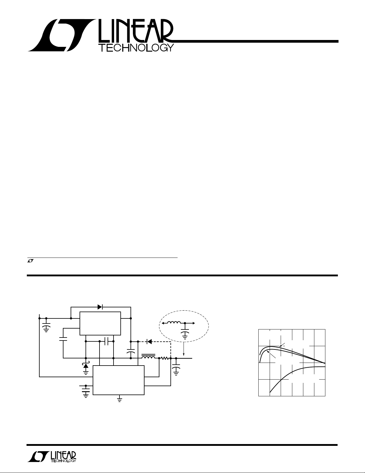
Figure 1. High Efficiency 5V Buck Converter
10µH
3A
100µF
16V
+
+
×
C2
390µF
16V
OPTIONAL
OUTPUT
FILTER
***
V
OUT
3.3V
3A
LT1432-3.3 TA01
100
LT1271, L = 30µH
VIN = 7V
90
80
EFFICIENCY (%)
70
60
0
0
Efficiency
D2 CONNECTED
TO OUTPUT
D2 CONNECTED
TO INPUT
Burst Mode OPERATION
(USE mA SCALE)
1A 2A
20mA
40mA
60mA
LT1432-3.3 TA02
3A
1
Page 2
LT1432-3.3
WU
U
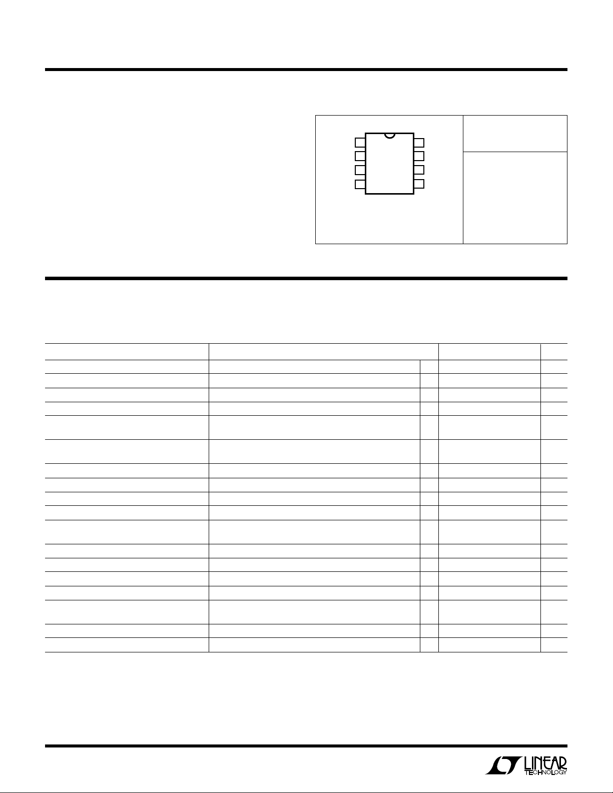
PACKAGE
/
O
RDER I FOR ATIO
1
2
3
4
TOP VIEW
V
LIM
V
OUT
V
IN
V
+
MODE
GND
V
C
DIODE
N8 PACKAGE
8-LEAD PDIP
8
7
6
5
S8 PACKAGE
8-LEAD PLASTIC SO
W
O
A
LUTEXI T
S
VIN Pin .................................................................... 30V
V+ Pin ..................................................................... 40V
A
WUW
ARB
U
G
I
S
ORDER PART
NUMBER
VC........................................................................... 35V
V
and V
LIM
Diode Pin Voltage ................................................... 30V
Pins................................................... 7V
OUT
LT1432CN8-3.3
LT1432CS8-3.3
Mode Pin Current (Note 2) ..................................... 1mA
Operating Temperature Range .................... 0°C to 70°C
Storage Temperature Range ................ –65°C to 150°C
Lead Temperature (Soldering, 10 sec)................. 300°C
LECTRICAL C CHARA TERIST
E
VC = 4V, VIN = 4V, V+ = 8V, V
Device is in standard test loop unless otherwise noted.
PARAMETER CONDITIONS MIN TYP MAX UNITS
Regulated Output Voltage VC Current = 220µA ● 3.24 3.30 3.36 V
Output Voltage Line Regulation VIN = 4V to 30V ● 520mV
Input Supply Current (Note 1) VIN = 4V to 30V, V+ = VIN + 5V, VC = VIN + 1V ● 0.3 0.5 mA
Quiescent Output Load Current 0.9 1.2 mA
Mode Pin Current V
Mode Pin Threshold Voltage I
(Normal to Burst)
VC Pin Saturation Voltage V
VC Pin Maximum Sink Current V
VC Pin Source Current V
Current Limit Sense Voltage (Note 3) Device in Current Limit Loop 56 60 64 mV
Pin Current Device in Current Limit Loop ● 30 45 70 µA
V
LIM
Supply Current in Shutdown V
Burst Mode Operation Output Ripple Device in Burst Test Circuit 100 mV
Burst Mode Operation Average Output Voltage Device in Burst Test Circuit ● 3.15 3.30 3.45 V
Clamp Diode Forward Voltage IF = 1mA, All Other Pins Open ● 0.5 0.65 V
Start-up Drive Current V
Restart Time Delay (Note 4) 0.7 1.2 10 ms
Transconductance, Output to VC Pin IC = 150µA to 250µA ● 2700 3600 5000 µmho
DIODE
= Open, V
ICS
= V
LIM
MODE
V
MODE
MODE
OUT
OUT
OUT
(Current Is Out of Pin)
MODE
OUT
V+ = VIN – 1V, VC = V
, V
OUT
= 0V (Current Is Out of Pin) ● 30 50 µA
= 3.3V (Shutdown) ● 15 30 µA
= 10µA (Out of Pin) ● 0.6 0.9 1.5 V
= 3.6V (Forced) ● 0.25 0.45 V
= 3.6V (Forced) ● 0.45 0.8 1.5 mA
= 3.0V (Forced) ● 35 60 100 µA
> 3V, VIN < 30V, VC and V+ = 0V 15 60 µA
= 1.5V (Forced), VIN = 4V to 26V, ● 30 45 mA
= 0V, TJ = 25°C
MODE
– 1.5V
IN
T
= 100°C, θJA = 150°C/W (N8)
JMAX
T
= 100°C, θJA = 170°C/W (S8)
JMAX
Consult factory for Military and Industrial grade parts.
p-p
2
Page 3
LT1432-3.3
LECTRICAL C CHARA TERIST
E
Operating parameters in standard circuit configuration.
VIN = 7V, I
PARAMETER CONDITIONS MIN TYP MAX UNITS
Burst Mode Operation Quiescent Input Supply Current 1.6 2.2 mA
Burst Mode Operation Output Ripple Voltage I
Normal Mode Equivalent Input Supply Current Extrapolated from I
Normal Mode Minimum Operating Input Voltage 100mA < I
Burst Mode Operation Minimum Operating Input Voltage 5mA < I
Efficiency Normal Mode I
Load Regulation Normal Mode 50mA < I
= 0, unless otherwise noted. These parameters guaranteed where indicated, but not tested.
OUT
ICS
= 0 80 mV
OUT
I
= 50mA 120 mV
OUT
= 20mA 3.0 mA
OUT
< 1.5A 4.5 V
OUT
< 50mA 4.1 V
OUT
= 0.5A 86 %
Burst Mode Operation I
Burst Mode Operation 0 < I
OUT
= 25mA 70 %
OUT
< 2A 5 15 mV
OUT
< 50mA 30 mV
OUT
p-p
p-p
The ● denotes specifications which apply over the full operating
temperature range.
Note 1: Does not include current drawn by the power IC. See operating
parameters in standard circuit.
Note 2: Breakdown voltage on the Mode pin is 7V. External current must
be limited to value shown.
U
T
S
CH
V
IN
V
IN
34
W
A
E
D2
V
CEQUIVALE
TI
V
SW
LT1271
V
C
+
V
C
65
V
GND
Note 3: Current limit sense voltage temperature coefficient is +0.33%/°C
to match TC of copper trace material.
Note 4: V
IN
FB
DIODE
pin switched from 3.6V to 3.0V.
OUT
OPTIONAL
CONNECTION
OF D2
V
OUT
2
–
S1**
V
60mV
LIM
1
+
3.3V
S3*
* S3 IS CLOSED ONLY DURING START-UP.
** S1 AND S2 ARE SHOWN IN NORMAL
MODE. REVERSE FOR Burst Mode
OPERATION.
Figure 2
S2**
MODE
CONTROL
MODE
8
+
–
7
GND
LT1432-3.3 F02
3
Page 4

LT1432-3.3
JUNCTION TEMPERATURE (°C)
0
SENSE VOLTAGE (mV)
60
70
100
LT1432-3.3 G9
50
40
25
50
75
80
* TEMPERATURE COEFFICIENT OF SENSE VOLTAGE IS
DESIGNED TO TRACK COPPER RESISTANCE.
OUTPUT CURRENT (A)
0
INPUT VOLTAGE (V)
5.5
6.0
6.5
4
LT1432-3.3 G03
5.0
4.5
4.0
1
2
3
5
TJ = 25°C
LT1171
LT1271
LT1270
DIODE
TO INPUT
LPER
Efficiency vs Input Voltage
100
TJ = 25°C
LT1271, L = 50µH
90
80
EFFICIENCY (%)
70
DIODE TO INPUT
I
OUT
R
F
O
DIODE TO OUTPUT
= 1A
ATYPICA
UW
CCHARA TERIST
E
C
Efficiency vs Load Current
95
TJ = 25°C
= 7V
V
IN
90
85
EFFICIENCY (%)
80
ICS
Minimum Input Voltage to Start –
Normal Mode (Diode to Input)
LT1270
LT1271
60
0
5101520
INPUT VOLTAGE (V)
Minimum Input Voltage –
Normal Mode (Diode to Output)
9.0
TJ = 25°C
8.0
7.0
LT1171 LT1271
6.0
INPUT VOLTAGE (V)
5.0
4.0
1
0
OUTPUT CURRENT (A)
2
DIODE
TO INPUT
3
Shutdown Current vs Input
Voltage
50
TJ = 25°C
25 30
LT1432-3.3 G01
4
LT1432-3.3 G04
75
0
0.5 1.0 1.5 2.0
LOAD CURRENT (A)
Minimum Running Voltage –
Normal Mode*
5.5
TJ = 25°C
5.0
4.5
4.0
INPUT VOLTAGE (V)
3.5
3.0
5
0
*SEE MINIMUM INPUT VOLTAGE TO START
LT1171
1
2
OUTPUT CURRENT (A)
Battery Current in Shutdown*
40
LT1271
LT1270
3
2.5 3.0
LT1432-3.3 G02
4
LT1432-3.3 G05
5
Burst Mode Operation Minimum
Input Voltage
5.5
TJ = 25°C
5.0
4.5
INPUT VOLTAGE (V)
4.0
3.5
10
0
LOAD CURRENT (mA)
30
20
Current Limit Sense Voltage*
40
LT1432-3.3 G06
50
40
30
20
CURRENT (µA)
10
0
0
5
4
10 15 20
INPUT VOLTAGE (V)
25 30
LT1432-3.3 G07
30
20
CURRENT (µA)
10
0
0
*DOES NOT INCLUDE LT1271 SWITCH LEAKAGE.
V
= 30V
IN
VIN = 6V
25
50
TEMPERATURE (°C)
75
100
LT1432-3.3 G08
Page 5

LPER
JUNCTION TEMPERATURE (°C)
0
TRANSCONDUCTANCE (µmho)
3000
4000
100
LT1432-3.3 G12
2000
1000
25
50
75
5000
Gm =
∆I(V
C
PIN)
∆V
OUT
MODE PIN VOLTAGE (V)
0
CURRENT (µA)
20
40
60
8
LT1432-3.3 G15
0
–20
–40
2
4
6
10
MODE DRIVE MUST
SINK ≈ 30µA AT 0V
TJ = 25°C
F
O
R
ATYPICA
UW
CCHARA TERIST
E
C
LT1432-3.3
ICS
Incremental Battery Current * in
Burst Mode Operation
2.0
TJ = 25°C
1.5
1.0
0.5
INCREMENTAL FACTOR (mA/mA)
0
* TO CALCULATE TOTAL BATTERY CURRENT IN Burst
Mode OPERATION, MULTIPLY LOAD CURRENT BY
INCREMENTAL FACTOR AND ADD NO-LOAD CURRENT.
5
0
BATTERY VOLTAGE (V)
15
10
20
LT1432-3.3 G10
Line Regulation
40
TJ = 25°C
20
No Load Battery Current in Burst
Mode Operation
5
TJ = 25°C
4
3
2
BATTERY CURRENT (mA)
1
25
0
5
0
BATTERY VOLTAGE (V)
15
20
10
25
LT1432-3.3 G11
Transconductance – V
Current
OUT
to V
C
Burst Mode Operation Load
Regulation
25
TJ = 25°C
V
IN
0
= 7V
Mode Pin Current
0
OUTPUT CHANGE (mV)
–20
–40
0
Restart Load Current
40
30
20
CURRENT (mA)
10
0
0
NORMAL MODE
Burst Mode OPERATION
5
V
= 4.5V
OUT
25
JUNCTION TEMPERATURE (°C)
10
INPUT VOLTAGE (V)
50
15
75
LT1432-3.3 G13
LT1432-3.3 G16
20
100
–25
OUTPUT CHANGE (mV)
–50
–75
20
0
LOAD CURRENT (mA)
60
80
40
100
LT1432-3.3 G14
Restart Time Delay Start-up Switch Characteristics
4
3
2
TIME DELAY (ms)
1
0
0
25
JUNCTION TEMPERATURE (°C)
50
75
100
LT1432-3.3 G16
5
TJ = 25°C
0
–20
–40
V+ PIN CURRENT (mA)
–60
–80
–1
–2
NOTE VERTICAL AND
HORIZONTAL SCALE
CHANGES AT 0,0
10
0
V+ TO VIN VOLTAGE
20
LT1432-3.3 G18
30
5
Page 6

LT1432-3.3
U
O
PPLICATI
A
More applications information on the LT1432-3.3 is available
in the LT1432 data sheet.
Basic Circuit Description
The LT1432-3.3 is a dedicated 3.3V buck converter driver
chip intended to be used with an IC switcher from the LT1171/
LT1271 family. This family of current mode switchers includes current ratings from 1.25A to 10A, and switching
frequencies from 40kHz to 100kHz as shown in the table
below.
SWITCH OUTPUT CURRENT IN
DEVICE CURRENT FREQUENCY BUCK CONVERTER
LT1270A 10A 60kHz 7.5A
LT1270 8A 60kHz 6A
LT1170 5A 100kHz 3.75A
LT1070 5A 40kHz 3.75A
LT1269 4A 100kHz 3A
LT1271 4A 60kHz 3A
LT1171 2.5A 100kHz 1.8A
LT1071 2.5A 40kHz 1.8A
LT1172 1.25A 100kHz 0.9A
LT1072 1.25A 40kHz 0.9A
The maximum load current which can be delivered by these
chips in a buck converter is approximately 75% of their
switch current rating. This is partly due to the fact that buck
converters must operate at very high duty cycles when input
voltage is low. The current mode nature of the LT1271 family
requires an internal reduction of peak current limit at high
duty cycles, so these devices are rated at only 80% of their full
current rating when duty cycle is 80%. A second factor is
inductor ripple current, half of which subtracts from maximum available load current. The LT1271 family was originally
intended for topologies which have the negative side of the
switch grounded, such as boost converters. It has an extremely efficient quasi-saturating NPN switch which mimics
the linear resistive nature of a MOSFET but consumes much
less die area. Driver losses are kept to a minimum with a
patented adaptive antisat drive that maintains a forced beta of
40 over a wide range of switch currents. This family is
attractive for high efficiency buck converters because of the
low switch loss, but to operate as a positive buck converter,
the GND pin of the IC must be floated to act as the switch
output node. This requires a floating power supply for the
chip and some means for level shifting the feedback signal.
The LT1432-3.3 performs these functions as well as adding
S
I FOR ATIO
WU
U
current limiting, micropower shutdown, and dual mode
operation for high conversion efficiency with both heavy and
very light loads.
The circuit in Figure 1 is a basic 3.3V positive buck
converter which can operate with input voltage from 4.5V
to 30V. The power switch is located between the VSW pin
and GND pin on the LT1271. Its current and duty cycle are
controlled by the voltage on the VC pin with respect to the
GND pin. This voltage ranges from 1V to 2V as switch
current increases from zero to full-scale. Correct output
voltage is maintained by the LT1432-3.3 which has an
internal reference and error amplifier (see Equivalent
Schematic in Figure 2). The amplifier output is level
shifted with an internal open collector NPN to drive the V
pin of the switcher. The normal resistor divider feedback
to the switcher feedback pin cannot be used because the
feedback pin is referenced to the GND pin, which is
switching up and down. The Feedback pin (FB) is simply
bypassed with a capacitor. This forces the switcher VC pin
to swing high with about 200µA sourcing capability. The
LT1432-3.3 VC pin then sinks this current to control the
loop. Transconductance from the regulator output to the
VC pin current is controlled to approximately 3600µmhos
by local feedback around the LT1432-3.3 error amplifier
(S2 closed in Figure 2). This is done to simplify frequency
compensation of the overall loop. A word of caution about
the FB pin bypass capacitor (C6): this capacitor value is
very non-critical, but the capacitor must be connected
directly to the GND pin or tab of the switcher to avoid
differential spikes created by fast switch currents flowing in the external PCB traces. This is also true for the
frequency compensation capacitor C5. C5 forms the
dominant loop pole.
A floating power supply for the switcher is generated by D2
and C3 which peak detect the input voltage during switch off
time. This is different than the 5V version of the LT1432 which
connects the anode of the diode to the output rather than the
input. The output connection is more efficient because the
floating voltage is a constant 5V (or 3.3V), independent of
input voltage, but in the case of the 3.3V circuit, minimum
required input voltage for starting is several volts higher (see
the Typical Performance Characteristics curves). When the
diode is connected to the input, the suggested type is a
C
6
Page 7

LT1432-3.3
PPLICATI
A
U
O
S
I FOR ATIO
WU
U
Schottky 1N5818. Diode type is more critical for the output
connection because the high capacitance of Schottky diodes
creates narrow output spikes. These spikes will be eliminated
if a secondary output filter is used or if there is sufficient lead
length between the regulator output and the load bypass
capacitors. Low capacitance diodes like the 1N4148 do not
create large spikes, but their high forward resistance requires
even higher input voltage to start.
D1, L1 and C2 act as the conventional catch diode and
output filter of the buck converter. These components
should be selected carefully to maintain high efficiency
and acceptable output ripple. See the original LT1432 (5V)
data sheet for detailed discussions of these parts.
Current limiting is performed by R2. Sense voltage is only
60mV to maintain high efficiency. This also reduces the
value of the sense resistor enough to utilize a printed
circuit board trace as the sense resistor. The sense voltage
has a positive temperature coefficient of 0.33%/°C to
match the temperature coefficient of copper.
The basic regulator has three different operating modes,
defined by the Mode pin drive. Normal operation occurs when
the Mode pin is grounded. A low quiescent current Burst
Mode operation can be initiated by floating the Mode pin.
Input supply current is typically 1.3mA in this mode, and
output ripple voltage is 100mV
. Pulling the Mode pin
p-p
above 2.5V forces the entire regulator into micropower
shutdown where it typically draws less than 20µA.
pulses. This maximizes efficiency at light load by eliminating
quiescent current in the switching IC during the period
between bursts.
The result of pulsating currents into the output capacitor
is that output ripple amplitude increases and ripple frequency becomes a function of load current. The typical
output ripple in Burst Mode operation is 100mVp-p, and
ripple frequency can vary from 50Hz to 2kHz. This is not
normally a problem for the logic circuits which are kept
alive during sleep mode.
Some thought must be given to proper sequencing between normal mode and Burst Mode operation. A heavy
(>100mA) load in Burst Mode operation can cause excessive output ripple, and an abnormally light load (10mA to
30mA, see Figure 3) in
normal
mode can cause the
regulator to revert to a quasi-Burst Mode operation that
also has higher output ripple. The worst condition is a
sudden, large increase in load current (>100mA) during
this quasi-Burst Mode operation or just after a switch
from Burst Mode operation to normal mode. This can
cause the output to sag badly while the regulator is
establishing normal mode operation (≈100µs). To avoid
problems, it is suggested that the power-down sequence
consist of reducing load current to below 100mA, but
greater than the minimum for normal mode, then switching to Burst Mode operation, followed by a reduction of
load current to the final sleep value. Power-up would
consist of increasing the load current to the minimum for
Burst Mode Operation
Burst Mode operation is initiated by allowing the Mode pin to
float, where it will assume a DC voltage of approximately 1V.
If AC pickup from surrounding logic lines is likely, the Mode
pin should be bypassed with a 200pF capacitor. Burst Mode
operation is used to reduce quiescent operating current when
the regulator output current is very low, as in sleep mode in
a lap-top computer. In this mode, hysteresis is added to the
error amplifier to make it switch on and off, rather than
maintain a constant amplifier output. This forces the switching IC to either provide a rapidly increasing current or to go
into full micropower shutdown. Current is delivered to the
output capacitor in pulses of higher amplitude and low duty
cycle rather than a continuous stream of low amplitude
Information furnished by Linear Technology Corporation is believed to be accurate and reliable.
However, no responsibility is assumed for its use. Linear Technology Corporation makes no representation that the interconnection of its circuits as described herein will not infringe on existing patent rights.
50
40
30
20
10
LOAD CURRENT – mA (NORMAL MODE)
0
4
Figure 3. Minimum Normal Mode Load Current
DIODE TO OUTPUT (1N5818)
DIODE TO INPUT (1N5818)
5
6
INPUT VOLTAGE (V)
NORMAL MODE
= 25°C
T
J
7
8
LT1432-3.3 • F03
9
7
Page 8

LT1432-3.3
PPLICATI
A
U
O
S
I FOR ATIO
WU
U
normal mode, then switching to normal mode, pausing for
1ms, followed by return to full load.
If this sequence is not possible, an alternative is to
increase the output capacitor to > 680µF. This modifica-
tion will often allow the power-down sequence to consist
of simultaneous turn-off of load current and switch to
Burst Mode operation. Power-up is accomplished by
switching to normal mode and simultaneously increasing
load current to the lowest possible value (30mA to 500mA),
followed by a short pause and return to full load current.
U
PACKAGE DESCRIPTIO
0.300 – 0.325
(7.620 – 8.255)
0.065
(1.651)
0.009 – 0.015
(0.229 – 0.381)
+0.025
0.325
–0.015
+0.635
8.255
()
–0.381
*THESE DIMENSIONS DO NOT INCLUDE MOLD FLASH OR PROTRUSIONS.
MOLD FLASH OR PROTRUSIONS SHALL NOT EXCEED 0.010 INCH (0.254mm)
TYP
(2.540 ± 0.254)
Dimensions in inches (millimeters) unless otherwise noted.
N8 Package
8-Lead Plastic DIP
0.045 – 0.065
(1.143 – 1.651)
0.005
(0.127)
MIN
0.100 ± 0.010
Full Shutdown
When the Mode pin is driven high, full shutdown of the
regulator occurs. Regulator input current will then consist
of the LT1432 shutdown current (≈15µA) plus the switch
leakage of the switching IC (≈1µA to 25µA). Mode input
current (≈15µA at 5V) must also be considered. Start-up
from shutdown can be in either normal or Burst Mode
operation, but one should always check start-up overshoot, especially if the output capacitor or frequency
compensation components have been changed.
0.130 ± 0.005
(3.302 ± 0.127)
0.125
(3.175)
MIN
0.018 ± 0.003
(0.457 ± 0.076)
0.015
(0.380)
MIN
0.255 ± 0.015*
(6.477 ± 0.381)
0.400*
(10.160)
MAX
876
1234
5
N8 0695
S8 Package
0.010 – 0.020
(0.254 – 0.508)
0.008 – 0.010
(0.203 – 0.254)
*
DIMENSION DOES NOT INCLUDE MOLD FLASH. MOLD FLASH
SHALL NOT EXCEED 0.006" (0.152mm) PER SIDE
**
DIMENSION DOES NOT INCLUDE INTERLEAD FLASH. INTERLEAD
FLASH SHALL NOT EXCEED 0.010" (0.254mm) PER SIDE
× 45°
0.016 – 0.050
0.406 – 1.270
0°– 8° TYP
0.053 – 0.069
(1.346 – 1.752)
0.014 – 0.019
(0.355 – 0.483)
8-Lead Plastic SOIC
0.004 – 0.010
(0.101 – 0.254)
0.050
(1.270)
BSC
0.228 – 0.244
(5.791 – 6.197)
0.189 – 0.197*
(4.801 – 5.004)
7
8
1
2
5
6
0.150 – 0.157**
(3.810 – 3.988)
3
SO8 0695
4
RELATED PARTS
PART NUMBER DESCRIPTION COMMENTS
LTC1148 High Efficiency Step-Down Switching Regulator Controller 5V Regulated Output Voltage
LT1432 High Efficiency Synchronous Step-Down Switching Regulator Adjustable and Fixed 5V or 3.3V Outputs
LT1507 1.5A, 500kHz Step-Down Switching Regulator Fixed Frequency PWM for Low Input Voltages from 4.5V to 12V
LT/GP 0895 2K REV A • PRINTED IN USA
LINEAR TECHNOLOGY CORPORATION 1992
8
Linear Technology Corporation
1630 McCarthy Blvd., Milpitas, CA 95035-7487
(408) 432-1900
●
FAX
: (408) 434-0507
●
TELEX
: 499-3977
 Loading...