

Page 1
LT1432
0
60
EFFICIENCY (%)
70
80
90
100
1A 2A
3A
20mA
LT1432 TA02
40mA
60mA
0
NORMAL MODE
(USE AMPS SCALE)
BURST MODE
(USE mA SCALE)
LT1271, L = 50µH
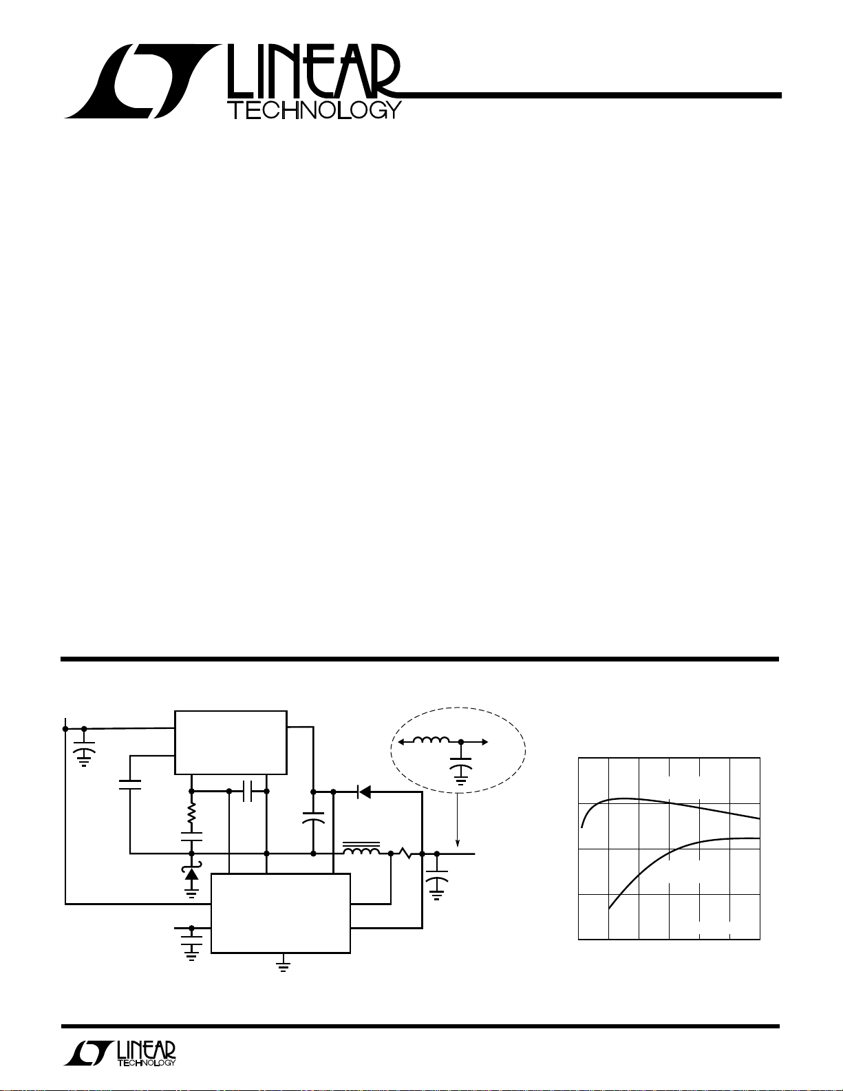
5V High Efficiency Step-Down
Switching Regulator Controller
EATU
F
■
Accurate Preset +5V Output
■
Up to 90% Efficiency
■
Optional Burst Mode for Light Loads
■
Can be Used with Many LTC Switching ICs
■
Accurate Ultra-Low-Loss Current Limit
■
Operates with Inputs from 6V to 30V
■
Shutdown Mode Draws Only 15µA
■
Uses Small 50µH Inductor
PPLICATI
A
■
Laptop and Palmtop Computers
■
Portable Data-Gathering Instruments
■
DC Bus Distribution Systems
■
Battery-Powered Digital Widgets
RE
S
O
U
S
DUESCRIPTIO
The LT1432 is a control chip designed to operate with the
LT1170/LT1270 family of switching regulators to make a
very high efficiency 5V step-down (buck) switching regulator. A minimum of external components is needed.
Included is an accurate current limit which uses only 60mV
sense voltage and uses “free” PC board trace material for
the sense resistor. Logic controlled electronic shutdown
mode draws only 15µA battery current. The switching
regulator operates down to 6V input.
The LT1432 has a logic controlled “burst” mode to achieve
high efficiency at very light load currents (0 to 100mA) such
as memory keep-alive. In normal switching mode, the
standby power loss is about 60mW, limiting efficiency at
light loads. In burst mode, standby loss is reduced to
approximately 15mW. Output current in this mode is
typically in the 5mA to 100mA range.
The LT1432 is available in 8-pin surface mount and DIP
packages. The LT1170/LT1270 family will also be available
in a surface mount version of the 5-pin TO-220 package.
For 3.3V versions contact Linear Technology Corporation.
V
IN
+
C1
330µF
35V
C6
0.02µF
MBR330p
MODE LOGIC
<0.3V = NORMAL MODE
>2.5V = SHUTDOWN
OPEN = BURST MODE
U
O
A
PPLICATITYPICAL
0.1µF
220pF
V
SW
LT1170
LT1271
FB
V
C
R1
680Ω
C4
D1
V
V
IN
MODE
0.03µF
C
C5
V
GND
DIODE
LT1432
IN
4.7µF
TANT
GND
D2
1N4148
C3
+
L1
50µH
+
V
V
LIM
V
OUT
* R2 IS MADE FROM PC BOARD
COPPER TRACES.
** MAXIMUM CURRENT IS DETERMINED
BY THE CHOICE OF LT1070 FAMILY.
SEE APPLICATION SECTION.
Figure 1. High Efficiency 5V Buck Converter
R2*
0.013Ω
10µH
3A
100µF
16V
+
+
×
C2
390µF
16V
OPTIONAL
OUTPUT
FILTER
V
OUT
5V
3A**
LT1432 TA01
Efficiency
1
Page 2

LT1432
WU
U
PACKAGE
/
O
RDER I FOR ATIO
W
O
A
LUTEXI T
S
VIN Pin .................................................................... 30V
V+ Pin ..................................................................... 40V
VC........................................................................... 35V
V
LIM
and V
Pins................................................... 7V
OUT
Diode Pin Voltage ................................................... 30V
Mode Pin Current (Note 2) ..................................... 1mA
Operating Temperature Range .................... 0°C to 70°C
Storage Temperature Range ................ –65°C to 150°C
Lead Temperature (Soldering, 10 sec.)................ 300°C
LECTRICAL C CHARA TERIST
E
VC = 6V, VIN = 12V, V+ = 10V, V
Device is in standard test loop unless otherwise noted.
PARAMETER CONDITIONS MIN TYP MAX UNITS
Regulated Output Voltage VC Current = 220µA ● 4.9 5.0 5.1 V
Output Voltage Line Regulation VIN = 6V to 30V ● 520 mV
Input Supply Current (Note 1) VIN = 6V to 30V, V+ = VIN + 5V, VC = VIN + 1V ● 0.3 0.5 mA
Quiescent Output Load Current 0.9 1.2 mA
Mode Pin Current V
Mode Pin Threshold Voltage I
(Normal to Burst)
VC Pin Saturation Voltage V
VC Pin Maximum Sink Current V
VC Pin Source Current V
Current Limit Sense Voltage (Note 3) Device in Current Limit Loop 56 60 64 mV
Pin Current Device in Current Limit Loop ● 30 45 70 µA
V
LIM
Supply Current in Shutdown V
Burst Mode Output Ripple Device in Burst Test Circuit 100 mV
Burst Mode Average Output Voltage Device in Burst Test Circuit ● 4.8 5 5.2 V
Clamp Diode Forward Voltage IF = 1mA, All Other Pins Open ● 0.5 0.65 V
Startup Drive Current V
Restart Time Delay (Note 4) 1 1.8 10 ms
Transconductance, Output to VC Pin IC = 150µA to 250µA ● 1500 2000 2800 µmho
The ● denotes specifications which apply over the operating temperature
range.
Note 1: Does not include current drawn by the LT1070 IC. See operating
parameters in standard circuit.
Note 2: Breakdown voltage on the mode pin is 7V. External current must
be limited to value shown.
A
WUW
= Open, V
DIODE
U
ARB
G
I
S
1
V
LIM
2
V
OUT
3
V
IN
+
4
V
8-LEAD PLASTIC DIP
8-LEAD PLASTIC SO
TOP VIEW
N8 PACKAGE
S8 PACKAGE
ORDER PART
MODE
8
GND
7
V
6
C
DIODE
5
NUMBER
LT1432CN8
LT1432CS8
ICS
= V
, V
LIM
OUT
= 0V (current is out of pin) ● 30 50 µA
MODE
V
= 5V (shutdown) ● 15 30 µA
MODE
= 10µA (out of pin) ● 0.6 0.9 1.5 V
MODE
= 5.5V (forced) ● 0.25 0.45 V
OUT
= 5.5V (forced) ● 0.45 0.8 1.5 mA
OUT
= 4.5V (forced) ● 40 60 100 µA
OUT
(current is out of pin)
> 3V, VIN < 30V, VC and V+ = 0V ● 15 60 µA
MODE
= 2.5V (forced), V+ = 5V to 25V, ● 30 45 mA
OUT
VIN = 6V to 26V, V+ = VIN – 1V, VC = V
= 0V, TJ = 25°C
MODE
– 1.5V
IN
Note 3: Current limit sense voltage temperature coefficient is +0.33%/°C
to match TC of copper trace material.
Note 4: V
pin switched from 5.5Vto 4.5V.
OUT
p-p
2
Page 3
LT1432
LECTRICAL C CHARA TERIST
E
Operating parameters in standard circuit configuration.
VIN = +12V, I
PARAMETER CONDITIONS MIN TYP MAX UNITS
Burst Mode Quiescent Input Supply Current 1.3 1.8 mA
Burst Mode Output Ripple Voltage I
Normal Mode Equivalent Input Supply Current Extrapolated from I
Normal Mode Minimum Operating Input Voltage 100mA < I
Burst Mode Minimum Operating Input Voltage 5mA < I
Efficiency Normal Mode I
Load Regulation Normal Mode 50mA < I
= 0, unless otherwise noted. These parameters guaranteed where indicated, but not tested.
OUT
ICS
= 0 100 mV
OUT
I
= 50mA 130 mV
OUT
= 20mA 6 mA
OUT
< 1.5A 6 V
OUT
< 50mA 6.2 V
OUT
= 0.5A 91 %
Burst Mode I
Burst Mode 0 < I
OUT
= 25mA 77 %
OUT
< 2A 10 25 mV
OUT
< 50mA 50 mV
OUT
p-p
p-p
U
T
V
IN
E
S
CH
V
IN
34
S3*
W
A
V
CEQUIVALE
TI
V
SW
LT1271
V
C
+
V
C
65
GND
V
IN
FB
DIODE
S1**
V
60mV
LIM
+5V
V
1
+
OUT
2
–
+
* S3 IS CLOSED ONLY DURING STARTUP.
** S1 AND S2 ARE SHOWN IN NORMAL
MODE. REVERSE FOR BURST MODE.
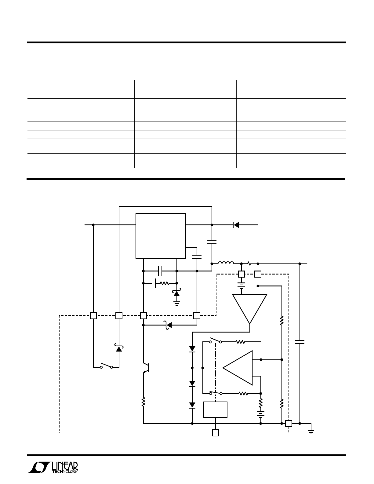
Figure 2
S2**
MODE
CONTROL
MODE
8
–
7
GND
LT1432 F02
3
Page 4
LT1432
JUNCTION TEMPERATURE (°C)
0
SENSE VOLTAGE (mV)
60
70
100
LT1432 G11
50
40
25
50
75
80
* TEMPERATURE COEFFICIENT OF SENSE VOLTAGE IS
DESIGNED TO TRACK COPPER RESISTANCE.
OUTPUT CURRENT (A)
0
INPUT VOLTAGE (V)
6.5
7.0
7.5
4
LT1432 G03
6.0
5.5
5.0
1
2
3
5
LT1270
LT1271
LT1270/1271
T
J
= 25°C
LPER
Efficiency vs Input Voltage
100
90
I
80
LOAD
I
LOAD
I
LOAD
F
= 2A
O
= 0.5A
= 1A
R
ATYPICA
UW
CCHARA TERIST
E
C
Efficiency vs Load Current
100
L = 50µH
90
LT1170
80
L = 25µH
LT1271
ICS
LT1270
L = 50µH
Minimum Input Voltage – Normal
Mode (1270/1271)
EFFICIENCY (%)
70
TJ = 25°C
LT1271, L = 50µH
60
0
5101520
INPUT VOLTAGE (V)
Minimum Input Voltage – Normal
Mode (1070 Family)
7.5
LT1070 FAMILY(40kHz)
= 25°C
T
J
7.0
6.5
6.0
INPUT VOLTAGE (V)
5.5
5.0
0
LT1072
LT1071
1
2
OUTPUT CURRENT (A)
LT1070
3
25 30
LT1432 G01
4
LT1432 G04
EFFICIENCY (%)
70
TJ = 25°C
60
0
0.5 1.0 1.5 2.0
LOAD CURRENT (A)
Minimum Input Voltage – Normal
Mode (1170 Family)
7.5
LT1170 FAMILY(100kHz)
= 25°C
T
J
7.0
LT1172
6.5
6.0
INPUT VOLTAGE (V)
5.5
5
5.0
0
LT1171
1
2
OUTPUT CURRENT (A)
2.5 3.0
LT1432 G02
Burst Mode Minimum Input
Voltage
7.0
TJ = 25°C
LT1170
3
4
5
LT1432 G05
6.5
LT1170
6.0
INPUT VOLTAGE (V)
5.5
5.0
10
0
LT1070
30
20
LOAD CURRENT (mA)
40
50
LT1432 G06
Shutdown Current vs Input
Voltage
50
TJ = 25°C
40
30
20
CURRENT (µA)
10
0
0
5
4
10 15 20
INPUT VOLTAGE (V)
25 30
LT1432 G07
Battery Current in Shutdown*
40
30
20
CURRENT (µA)
10
0
0
*DOES NOT INCLUDE LT1271 SWITCH LEAKAGE.
V
= 30V
IN
VIN = 6V
25
50
TEMPERATURE (°C)
75
Current Limit Sense Voltage*
100
LT1432 G08
Page 5
LPER
MODE PIN VOLTAGE (V)
0
CURRENT (µA)
20
40
60
8
LT1432 G15
0
–20
–40
2
4
6
10
MODE DRIVE MUST
SINK ≈ 30µA AT 0V
TJ = 25°C
V+ TO VIN VOLTAGE
–2
V+ PIN CURRENT (mA)
–20
0
5
20
LT1432 G18
–40
–60
–80
–1
0
10
30
TJ = 25°C
NOTE VERTICAL &
HORIZONTAL SCALE
CHANGES AT 0,0
F
O
R
ATYPICA
UW
CCHARA TERIST
E
C
LT1432
ICS
Incremental Battery Current * in
Burst Mode
2.0
TJ = 25°C
1.5
1.0
0.5
INCREMENTAL FACTOR (mA/mA)
0
* TO CALCULATE TOTAL BATTERY CURRENT IN BURST
MODE, MULTIPLY LOAD CURRENT BY INCREMENTAL
FACTOR AND ADD NO-LOAD CURRENT.
5
0
BATTERY VOLTAGE (V)
15
20
10
25
LT1432 G10
Line Regulation
40
TJ = 25°C
BURST MODE
20
No Load Battery Current in Burst
Mode
5
TJ = 25°C
4
3
2
BATTERY CURRENT (mA)
1
0
5
0
BATTERY VOLTAGE (V)
15
10
Burst Mode Load Regulation
25
TJ = 25°C
0
20
LT1432 G09
Transconductance – V
OUT
to V
C
Current
4000
3000
2000
1000
TRANSCONDUCTANCE (µmho)
25
40
∆I(V
PIN)
C
Gm =
∆V
OUT
0
25
JUNCTION TEMPERATURE (°C)
50
75
100
LT1432 G12
Mode Pin Current
0
OUTPUT CHANGE (mV)
–20
–40
40
30
20
CURRENT (mA)
10
0
NORMAL MODE
0
5
10
INPUT VOLTAGE (V)
Restart Load Current
V
= 4.5V
OUT
0
25
JUNCTION TEMPERATURE (°C)
50
–25
OUTPUT CHANGE (mV)
–50
15
75
20
LT1432 G13
100
LT1432 G16
–75
20
0
Restart Time Delay
4
3
2
TIME DELAY (ms)
1
0
0
25
JUNCTION TEMPERATURE (°C)
60
40
LOAD CURRENT (mA)
50
80
100
LT1432 G14
Startup Switch Characteristics
75
100
LT1432 G16
5
Page 6
LT1432
U
O
PPLICATI
A
Basic Circuit Description
The LT1432 is a dedicated 5V buck converter driver chip
intended to be used with an IC switcher from the LT1070
family. This family of current mode switchers includes
current ratings from 1.25A to 10A, and switching frequencies from 40kHz to 100kHz as shown in the table below.
SWITCH OUTPUT CURRENT IN
DEVICE CURRENT FREQUENCY BUCK CONVERTER
LT1270A 10A 60kHz 7.5A
LT1270 8A 60kHz 6A
LT1170 5A 100kHz 3.75A
LT1070 5A 40kHz 3.75A
LT1271 4A 60kHz 3A
LT1171 2.5A 100kHz 1.8A
LT1071 2.5A 40kHz 1.8A
LT1172 1.25A 100kHz 0.9A
LT1072 1.25A 40kHz 0.9A
The maximum load current which can be delivered by
these chips in a buck converter is approximately 75% of
their switch current rating. This is partly due to the fact that
buck converters must operate at very high duty cycles
when input voltage is low. The “current mode” nature of
the LT1070 family requires an internal reduction of peak
current limit at high duty cycles, so these devices are rated
at only 80% of their full current rating when duty cycle is
80%. A second factor is inductor ripple current, half of
which subtracts from maximum available load current.
See Inductor Selection for details. The LT1070 family was
originally intended for topologies which have the negative
side of the switch grounded, such as boost converters. It
has an extremely efficient quasi-saturating NPN switch
which mimics the linear resistive nature of a MOSFET but
consumes much less die area. Driver losses are kept to a
minimum with a patented adaptive antisat drive that maintains a forced beta of 40 over a wide range of switch
currents. This family is attractive for high efficiency buck
converters because of the low switch loss, but to operate
as a positive buck converter, the ground pin of the IC must
be floated to act as the switch output node. This requires
a floating power supply for the chip and some means for
level shifting the feedback signal. The LT1432 performs
these functions as well as adding current limiting, micropower shutdown, and dual mode operation for high
conversion efficiency with both heavy and very light loads.
S
I FOR ATIO
WU
U
The circuit in Figure 1 is a basic 5V positive buck converter
which can operate with input voltage from 6V to 30V. The
power switch is located between the VSW pin and GND pin
on the LT1271. Its current and duty cycle are controlled by
the voltage on the VC pin with respect to the GND pin. This
voltage ranges from 1V to 2V as switch current increases
from zero to full scale. Correct output voltage is maintained by the LT1432 which has an internal reference and
error amplifier (see Equivalent Schematic in Figure 2). The
amplifier output is level shifted with an internal open
collector NPN to drive the VC pin of the switcher. The
normal resistor divider feedback to the switcher feedback
pin cannot be used because the feedback pin is referenced
to the GND pin, which is switching up and down. The
feedback pin (FB) is simply bypassed with a capacitor.
This forces the switcher VC pin to swing high with about
200µA sourcing capability. The LT1432 VC pin then sinks
this current to control the loop. Transconductance from
the regulator output to the VC pin current is controlled to
approximately 2000µmhos by local feedback around the
LT1432 error amplifier (S2 closed in Figure 2). This is done
to simplify frequency compensation of the overall loop. A
word of caution about the FB pin bypass capacitor (C6):
this capacitor value is very non-critical, but the capacitor
must be connected directly to the GND pin or tab of the
switcher to avoid differential spikes created by fast switch
currents flowing in the external PCB traces. This is also
true for the frequency compensation capacitors C4 and
C5. C4 forms the dominant loop pole with a loop zero
added by R1. C5 forms a higher frequency loop pole to
control switching ripple at the VC pin.
A floating 5V power supply for the switcher is generated by
D2 and C3 which peak detect the output voltage during
switch “off” time. The diode used for D2 is a low capacitance type to avoid spikes at the output. Do not substitute
a Schottky diode for D2 (they are high capacitance). This
is a very efficient way of powering the switcher because
power drain does not increase with regulator input voltage. However, the circuit is not self-starting, so some
means must be used to start the regulator. This is performed by the internal current path of the LT1432 which
allows current to flow from the input supply to the V+ pin
during startup.
6
Page 7
LT1432
P
VV V I
V
FIN–OUT OUT
IN
=
()()
U
O
PPLICATI
A
D1, L1 and C2 act as the conventional catch diode and
output filter of the buck converter. These components
should be selected carefully to maintain high efficiency
and acceptable output ripple. See other sections of this
data sheet for detailed discussions of these parts.
Current limiting is performed by R2. Sense voltage is only
60mV to maintain high efficiency. This also reduces the
value of the sense resistor enough to utilize a printed
circuit board trace as the sense resistor. The sense voltage
has a positive temperature coefficient of 0.33%/°C to
match the temperature coefficient of copper. See Current
Limiting section for details.
The basic regulator has three different operating modes,
defined by the mode pin drive. Normal operation occurs
when the mode pin is grounded. A low quiescent current
“burst” mode can be initiated by floating the mode pin.
Input supply current is typically 1.3mA in this mode, and
output ripple voltage is 100mV
above 2.5V forces the entire regulator into micropower
shutdown where it typically draws less than 20µA. See
Mode Pin Drive for details.
Efficiency
Efficiency in normal mode is maximum at about 500mA
load current, where it exceeds 90%. At lower currents, the
operating supply current of the switching IC dominates
losses. The power loss due to this term is approximately
8mA × 5V, or 40mW. This is 4% of output power at a load
current of 200mA. At higher load currents, losses in the
switch, diode, and inductor series resistance begin to
increase as the square of current and quickly become the
dominant loss terms.
Loss in inductor series resistance;
P = RS (I
Loss in switch on resistance;
VRI
P
=
Loss in switch driver current;
)
OUT
()
OUT SW
S
I FOR ATIO
2
2
()
OUT
V
IN
p-p
WU
. Pulling the mode pin
U
IV
()
OUT OUT
P
=
40V
Diode loss;
(Use
VF vs I
I
)
OUT
RS = Inductor series resistance
RSW = Switch resistance of LT1271, etc.
IF = Diode current
VF = Diode forward voltage at IF = I
Inductor core loss depends on peak-to-peak ripple current
in the inductor, which is independent of load current for
any load current large enough to establish continuous
current in the inductor. Believe it or not, core loss is also
independent of the physical size of the core. It depends
only on core material, inductance value, and switching
frequency for fixed regulator operating conditions. Increasing inductance or switching frequency will reduce
core loss, because of the resultant decrease in ripple
current. For high efficiency, low loss cores such as ferrites
or Magnetics Inc. molypermalloy or KoolMµ are recommended. The lower cost Type 52 powdered iron from
Phillips is acceptable only if larger inductance is used and
the increased size and slight loss in efficiency is acceptable. In a typical buck converter using the LT1271 (60kHz)
with a 12V input, and a 50µH inductor, core loss with a
Type 52 powdered iron core is 203mW. A molypermalloy
core reduces this figure to 28mW. With a 1A output, this
translates to 4% and 0.56% core loss respectively – a big
difference in a high efficiency converter. For details on
inductor design and losses, see Application Note 44.
What are the benefits of using an active (synchronous)
switch to replace the catch diode? This is the trendy thing
to do, but calculations and actual breadboards show that
the improvement in efficiency is only a few percent at best.
This can be shown with the following simplified formulas:
Diode Loss
F
2
IN
graph on diode data sheet, assuming IF =
OUT
VV V I
()()
FIN–OUT OUT
=
V
IN
7
Page 8
LT1432
U
O
PPLICATI
A
FET Switch Loss
(Ignoring gate drive power)
The change in efficiency is:
Diode Loss – FET Loss Efficiency
()()
This is equal to:
V–V V–R I E
()
IN OUT F FET OUT
If VF (diode forward voltage) = 0.45V, VIN = 10V, V
R
= 0.1Ω, I
FET
ment in efficiency is only:
10V – 5V 0.45V – 0.1 1A 0.9
()
This does not take FET gate drive losses into account,
which can easily reduce this figure to less than 2%. The
added cost, size, and complexity of a synchronous switch
configuration would be warranted only in the most extreme circumstances.
Burst mode efficiency is limited by quiescent current drain
in the LT1432 and the switching IC. The typical burst mode
zero-load input power is 27mW. This gives about one
month battery life for a 12V, 1.2AHr battery pack. Increasing load power reduces discharge time proportionately.
Full shutdown current is only about 15µA, which is considerably less than the self-discharge rate of typical batteries.
Burst Mode Operation
Burst mode is initiated by allowing the mode pin to float,
where it will assume a DC voltage of approximately 1V. If
AC pickup from surrounding logic lines is likely, the mode
pin should be bypassed with a 200pF capacitor. Burst
mode is used to reduce quiescent operating current when
the regulator output current is very low, as in “sleep” mode
OUT
()()
S
I FOR ATIO
VV R I
()()()
IN–OUT SW OUT
=
VV
()( )
IN OUT
×
()()
VV
()( )
IN OUT
= 1A, and efficiency = 90%, the improve-
10V 5V
()()
×
Ω
WU
V
IN
2
2
OUT
2
2.8%
=
U
2
= 5V,
in a lap-top computer. In this mode, hysteresis is added to
the error amplifier to make it switch on and off, rather than
maintain a constant amplifier output. This forces the
switching IC to either provide a rapidly increasing current
or to go into full micropower shutdown. Current is delivered to the output capacitor in pulses of higher amplitude
and low duty cycle rather than a continuous stream of low
amplitude pulses. This maximizes efficiency at light load
by eliminating quiescent current in the switching IC during
the period between bursts.
The result of pulsating currents into the output capacitor
is that output ripple amplitude increases, and ripple frequency becomes a function of load current. The typical
output ripple in burst mode is 150mVp-p, and ripple
frequency can vary from 50Hz to 2kHz. This is not normally
a problem for the logic circuits which are kept “alive”
during sleep mode.
Some thought must be given to proper sequencing between normal mode and burst mode. A heavy (>100mA)
load in burst mode can cause excessive output ripple, and
an abnormally light load (10mA to 30mA, see curves) in
normal mode can cause the regulator to revert to a quasiburst mode that also has higher output ripple. The worst
condition is a sudden, large increase in load current
(>100mA) during this quasi-burst mode or just after a
switch from burst mode to normal mode. This can cause
the output to sag badly while the regulator is establishing
normal mode operation (≈100µs). To avoid problems, it is
suggested that the power-down sequence consist of reducing load current to below 100mA, but greater than the
minimum for normal mode, then switching to burst mode,
followed by a reduction of load current to the final sleep
value. Power-up would consist of increasing the load
current to the minimum for normal mode, then switching
to normal mode, pausing for 1ms, followed by return to
full load.
If this sequence is not possible, an alternative is to
minimize normal mode settling time by adding a 47kΩ
resistor between V+ and VC pins. The output capacitor
should be increased to >680µF and the compensation
capacitors should also be as small as possible, consistent
with adequate phase margin. These modifications will
8
Page 9
LT1432
PPLICATI
A
U
O
S
I FOR ATIO
WU
U
often allow the power-down sequence to consist of simultaneous turn-off of load current and switch to burst mode.
Power-up is accomplished by switching to normal mode
and simultaneously increasing load current to the lowest
possible value (30mA to 500mA), followed by a short
pause and return to full load current.
Full Shutdown
When the mode pin is driven high, full shutdown of the
regulator occurs. Regulator input current will then consist
of the LT1432 shutdown current (≈15µA) plus the switch
leakage of the switching IC (≈1µA to 25µA). Mode input
current (≈15µA at 5V) must also be considered. Startup
from shutdown can be in either normal or burst mode, but
one should always check startup overshoot, especially if
the output capacitor or frequency compensation components have been changed.
5V/DIV
0
1A/DIV
0
5µs/DIV
Figure 3
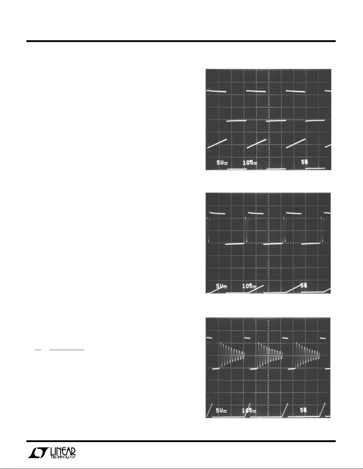
Switching Waveforms in Normal Mode
The waveforms in Figures 3 through 10 were taken with
an input voltage of 12V. Figure 3 shows the classic buck
converter waveforms of switch output voltage (5V/DIV) at
the top and switch current (1A/DIV) underneath, at an
output current of 2A. The regulator is operating in “continuous” mode as evidenced by the fact that switch
current does not start at zero at switch turn-on. Instead,
it jumps to an initial value, then continues to slope upward
during the duration of switch on time. The slope of the
current waveform is determined by the difference between input and output voltage, and the value of inductor
used.
V–V
()
dl
dt
=
IN OUT
L
According to theory, the average switch current during
switch on time should be equal to the 2A output current
and this is confirmed in the photograph. The peak switch
current, however, is about 2.4A.This peak current must
be considered when calculating maximum available load
current because both the LT1432 and the LT1070 family
current limit on instantaneous switch current.
5V/DIV
1A/DIV
5V/DIV
0.5A/DIV
0
0
0
0
5µs/DIV
Figure 4
5µs/DIV
Figure 5
9
Page 10

LT1432
U
O
PPLICATI
A
Note that the switch output voltage is nearly identical to
the 12V input during switch on time, a necessary requirement for high efficiency, and indicative of an efficient
switch topology. Also note the fast, clean edges on the
switching waveforms, an additional requirement for high
efficiency. The “overlap time” of switch current and voltage, which leads to AC switching losses, is only 10ns.
Figure 4 shows the same waveforms when load current
has been reduced to 0.25A, and Figure 5 is at 25mA (note
the scale change for current in Figure 5). The regulator is
now into discontinuous mode as shown by the fact that
switch current has no initial jump, but starts its upward
slope from zero. This implies that the inductor current has
dropped to zero during switch off time, and that is shown
by the “ringing” waveform on the rising edge of switch
voltage. The switch has not yet been turned on, but the
voltage at its output rises and rings as the “input” end of
the inductor tries to settle to the same voltage as its
“output” end (5V).
S
I FOR ATIO
WU
U
1A/DIV
5µs/DIV
Figure 6. Input Capacitor Current
This ringing is not an oscillation.
energy in the catch diode capacitance. This energy is
transferred to the inductor as the inductor voltage attempts to rise to 5V. The inductor and diode capacitance
tank circuit continues to ring until the stored energy is
dissipated by losses in the core and parasitic resistances.
The relatively undamped nature in this case is good
because it shows low losses and that translates to high
efficiency. EMI is not increased by operating in this mode.
Figure 6 shows input capacitor current (1A/DIV) with I
= 2A. The theoretical peak-to-peak value (ignoring sloping
waveforms) is equal to output current, and this is indeed
what the top waveform shows. The RMS value is approximately equal to one half output current. This is a major
consideration because the physical size of a capacitor with
1A ripple current rating may make it the largest component
in the regulator (see output capacitor section). Clever
desigers may hit on the idea of utilizing battery impedance
or remote input capacitors to divert some of the current
away from the actual local capacitor to reduce its size. This
is not too practical as shown by the middle waveform in
Figure 6, which shows input capacitor current when an
additional large capacitor is added about 6" away from the
It is the result of stored
OUT
0.5A/DIV
5µs/DIV
Figure 7. Output Capacitor Ripple Current
local capacitor. The wiring inductance and parasitic resistance limit the shunting effect and local capacitor current
is reduced only slightly. the bottom waveform shows input
capacitor current with output current reduced to 0.25A.
Figure 7 shows output capacitor ripple current at loads of
2A, 0.25A, and 25mA respectively starting from the top.
Note that ripple current is independent of load current until
the load drops well into the discontinuous region. The
small steps superimposed on the triangular ripple are
caused by loading of the diode which pumps the power
supply capacitor on the LT1271. Amplitude of the ripple
current is about 0.7Ap-p in this case, or approximately
10
Page 11

LT1432
U
O
PPLICATI
A
0.2A RMS. Theoretically the output capacitor size would
be minimized by using one which just met this ripple
current, but in practice, this would yield such high output
ripple voltage that an additional output filter would have to
be added. A better solution in the case of buck converters
is usually just to increase the size of the output capacitor
to meet output ripple voltage requirements.
50mV/DIV
1A/DIV
0
Figure 8. Output Ripple Current
1A/DIV
S
I FOR ATIO
5µs/DIV
WU
U
tures, so be sure to check ESR ratings at the lowest
expected operating temperature. Ripple voltage can be
reduced by increasing the inductor value, but this has
rapidly diminishing returns because of typical size restraints.
Figure 9 shows diode current under normal load conditions of 2A, and with the output shorted. Current limit has
been set at 3A. Average diode current at I
about 1A because of duty cycle considerations. Under
short circuit conditions, duty cycle is nearly 100% for the
diode (switch duty cycle is near zero), and diode average
current is nearly 3A. Designs which must tolerate continuous short circuit conditions should be checked carefully
for diode heating. Foldback current limiting can be used if
necessary.
Figure 10 shows inductor current (0.5A/DIV) with a 2A and
100mA load. Average inductor current is always equal to
output current, but it is obvious that with 100mA load,
inductor current drops to zero for part of the switching
cycle, indicating dicontinuous mode. When selecting an
inductor, keep in mind that RMS current determines
copper losses, peak-to-peak current determines core loss,
and peak current must be calculated to avoid core saturation. Also, remember that during short circuit conditions,
inductor current will increase to the full current limit value.
Inductor failure is normally caused by overheating of the
winding insulation with resultant turn-to-turn shorts.
Foldback current limiting will be helpful.
= 2A is only
OUT
0
1A/DIV
0
Figure 9. Diode Current
Figure 8 shows output ripple voltage at the top and switch
current below. Peak-to-peak ripple voltage is 80mV. This
implies an output capacitor effective series resistance
(ESR) of 80mV/0.7A = 0.11Ω. Capacitor ESR varies significantly with temperature, increasing at low tempera-
5µs/DIV
0.5A/DIV
0
Figure 10. Inductor Current
5µs/DIV
11
Page 12

LT1432
U
O
PPLICATI
A
Switching Waveforms in Burst Mode
In burst mode, the LT1432 amplifier is converted to a
comparator with hysteresis. This causes its VC pin current
drive to be either zero (output low), or full “on” at about
0.8mA (output high). The LT1271 therefore is either driven
to full on condition or forced into complete micropower
shutdown. This makes a dramatic reduction in quiescent
current losses because the switching regulator chip draws
supply current only during the relatively short “on” periods. This burst mode results in a battery drain of only
1.2mA with zero output load, even though the nominal
quiescent current of the switcher chip is 7mA. This low
battery drain is accomplished at the expense of higher
output ripple voltage, but the ripple is still well within the
normal requirements for logic chips.
Figure 11 shows burst mode output ripple at load currents
of 0 (top trace), and 50mA (bottom trace). Ripple amplitude is nominally set by the 100mV hysteresis built into the
LT1432, but in most applications, other effects come into
play which can significantly modify this value. The first is
delay in turning off the switcher. This causes the output to
overshoot slightly and therefore increases output ripple.
Delay is caused by the compensation capacitors used to
maintain a stable loop in the normal mode. Another effect,
however, is the ESR of the output capacitor. The surge
current from the switcher creates a step across the capacitor ESR which prematurely trips the LT1432 comparator,
reducing
turning the switcher back on when the output falls below
its lower level. This delay is somewhat longer, but because
the output normally falls at a much slower rate than it rises,
this delay is not significant until output current exceeds
10mA. Falling rate is set by the output capacitor (including
any secondary filter capacitor), and the actual load current, dV
implies a load current of approximately 2mA. This is the
sum of the 1mA output quiescent current of the LT1432
and the 1mA drawn by the VC pin and shunted through the
internal Schottky diode during the switcher “off” period.
The bottom trace at I
caused by turn-on delay. Note that ripple frequency has
increased from 50Hz to about 600Hz and amplitude has
ripple amplitude. A second delay occurs in
/dt = I
OUT
S
I FOR ATIO
OUT/COUT
. The slope in the top traces
= 50mA shows increased ripple
OUT
WU
U
100mV/DIV
100mV/DIV
5ms/DIV
Figure 11. Burst Mode Output Ripple Voltage
100mV/DIV
100mV/DIV
5ms/DIV
Figure 12. Burst Mode Output Ripple Voltage
more than doubled. Figure 12 shows the same conditions
except that a 47kΩ resistor is connected from the LT1271
VIN pin to the VC pin to provide more start-up current.
These additions reduce ripple amplitude at 50mA load
current to a value only slightly higher than the no-load
condition.
Although it is difficult to see in Figures 11 and 12, there is
a narrow spike on the leading edge of the ripple caused by
the burst current and capacitor ESR. Figure 13 shows this
spike in more detail, both with and without an output filter.
12
Page 13

LT1432
PPLICATI
A
100mV/DIV
100mV/DIV
U
O
S
FROM
INDUCTOR
WU
I FOR ATIO
50µs/DIV
Figure 13
“L” IS MEASURED FROM
POINT “X” TO POINT “Y”
U
Current Limiting
The LT1432 has true switching current limit with a sense
voltage of 60mV. This low sense voltage is used to
maintain high efficiency with normal loads and to make it
possible to use the printed circuit board trace material as
the sense resistor. The sense resistor value must take
ripple current into account because the LT1432 limits on
the peak of the inductor ripple current. Errors in the sense
resistor must also be allowed for.
V
R
SENSE
R
SENSE
V
SENSE
I
MAX
=
= Required sense resistor
= 60mV
= Maximum load current, including any surge
SENSE
I
I1.2*+
()
MAX
RIP
2
longer than 50µs
* 1.2 is a fudge factor for errors in R
SENSE
and V
SENSE
.
TO V
LIM
PIN
TO V
OUT
PIN
Figure 14. PC trace Current Limit Sense Resistor
with Kelvin Contacts
“X”
“Y”
TO LOAD
“W”
KEEP THIS DISTANCE SHORT
FOR BEST LOAD REGULATION.
}
LT 432 F14
Time scale has been expanded to 50µs/DIV. The spike
consists of several switching cycles of the LT1271 as
shown in the lower trace. In the upper trace, the output
filter has smoothed the switching frequency content of the
spike, but the actual spike amplitude is only modestly
reduced. Increasing the output filter constants from 10µH
and 220µF to 20µH and 330µF would eliminate most of
the spike.
I
RIP
= 1/2 Peak to Peak Inductor Ripple Current
2
VV–V
()
OUT IN OUT
=
2V (f)(L)
IN
f = Frequency
L = Inductance
Use VIN maximum
Example: I
= 2A, f = 60kHz, maximum VIN = 15V,
MAX
L = 50µH;
515–5
I
RIP
=
2
2 15 60E 50E
R=
SENSE
The formula for R
()
3–6
()
60mV
2A 1.2 + 0.55A
()
shows a 1.2 multiplier term in the
SENSE
0.55A
=
0.02
=Ω
denominator which makes typical current limit 20% above
full load current. This accounts for small errors in the PCB
trace resistance. Trace resistance errors are kept to a
minimum by using internal traces (on multilayer boards)
13
Page 14

LT1432
PPLICATI
A
U
O
S
I FOR ATIO
WU
U
because these traces do not have errors caused by plating
operations. The suggested trace width for 1/2oz foil is
0.03" for each 1A of current limit to keep trace temperature
rise reasonable. 3A current limit would require the width
to be 0.09". 1oz foil can reduce trace width to 0.02" per
amp. Inductance in the trace is not critical so the trace can
be wound serpentine or any other shape that fits available
space. Kelvin connections should be used as shown in
Figure 14 to avoid errors due to termination resistance.
The length of the sense resistor trace can be calculated
from:
WR
()
Length =
SENSE
R
CU
Inches
W = width of copper trace (≈0.03" per amp for 1/2oz
copper foil)
RCU = resistivity of PCB trace, expressed as Ω per square.
It is found by calculating the resistance of a section of trace
with equal length and width. For typical 1/2oz material,
RCU is approximately 1mΩ per square. In the example
shown above, with width = 2A times 0.03" = 0.06";
0.06 0.02
Length =
()
= 1.2 Inches
0.001
Current limiting maintains true switching action, but power
dissipation in the IC switch and catch diode will shift
depending on output voltage. At output voltages near the
correct regulated value, power will be distributed between
switch and the diode according to the usual calculations.
Under short circuit conditions, switch duty cycle will drop
to a very low value, and power will concentrate in the
diode, which will be running at near 100% duty cycle. If
continuous shorts must be tolerated, the catch diode must
be sized to handle the full current limit value, or foldback
current can be used.
Foldback Current Limiting
Foldback current limiting makes the short circuit current
limit somewhat lower than the full load current limit to
reduce component stress under short circuit conditions.
This is shown in Figure 15 with the addition of R3 and R4.
The voltage drop across R3 adds to the 60mV current limit
V
IN
6V – 25V
+
C1
200µF
35V
<0.3V = NORMAL MODE
>2.5V = SHUTDOWN
OPEN = BURST MODE
C6
0.02µF
0.1µF
D1
MBR330p
220pF
V
SW
LT1271
FB
V
C
R1
680Ω
C4
V
C
V
IN
MODE
C5
0.03µF
GND
DIODE
LT1432
V
IN
4.7µF
TANT
GND
C3
+
+
V
V
LIM
V
OUT
Figure 15. Adding Foldback Current Limiting
L1
50µH
D2
1N4148
R2
0.025Ω
R3
100Ω
R4
12.5k
+
10µH
3A
100µF
16V
C2
470µF
16V
+
×
OPTIONAL
OUTPUT
FILTER
V
OUT
5V
3A
LT1432 F15
14
Page 15

LT1432
R4 =
5V 100
100mV – 60mV+100 40 A – 0.042 0.55
7.45k
Ω
Ω
Ω
()
() ()
=
µ
=
()
+
()()
=
60mV – 40 A 100 5V
100
7.45k
0.042 0.55
0.042
2.38A
µΩ
Ω
U
O
PPLICATI
A
voltage. This extra sense voltage is set by output voltage
and R4 under normal loads, but drops to near zero when
the output is shorted.
The 40µA bias current flowing out of the V
accounted for when calculating a value for R4. This current
flows through R3, causing a 4mV
voltage for R3 = 100Ω. The following formulas define
current limit conditions:
Current limit at V
60mV –I R3 + V
=
Short Circuit Current =
R =
SENSE
R4 =
VS = Desired full load sense voltage.
I
= Peak load current (for any time greater than
MAX
50µs)
IB = V
To maintain high efficiency and avoid any startup problems with loads that have non-linear V/I characteristics, a
100mV (average) sense voltage is suggested for foldback
current limiting. The suggested value for R3 is 100Ω. This
is a compromise value to keep errors due to V
current low, and to minimize current drain on the output
created by the R3/R4 path. From the previous design
example, with I
R3 = 100Ω, V
R =
SENSE
B OUT SENSE
I (1.2)
V – 60mV +I R3 + R
S B SENSE
pin bias current (≈40mA)
LIM
MAX
LIM
S
I FOR ATIO
= 5V
OUT
()( )
V
LIM
MAX
VR3
OUT
R3
R4
R
SENSE
60mV –I (R3)
R
()
()( )
= 2A and I
= 100mV:
100mV
2A 1.2
=Ω
()
/2 = 0.55A, and assuming
RIP
0.042
WU
LIM
decrease
R
–
()
B
SENSE
I
RIP
2
U
pin must be
in sense
I
RIP
2
bias
LIM
Current limit at V
Current limit (output shorted)
60mV – 100 40 A
=
0.042
Minimum Input Voltage
Minimum input voltage for a buck converter using the
LT1432 is actually limited by the IC switcher used with it.
There are three factors which contribute to the minimum
voltage. At very light loads, the charge pump technique
used to provide the floating power for the switcher chip is
unable to provide sufficient current. See Figure 16 for the
minimum load required as a function of input voltage
when operating in the normal mode.
At moderate to heavy loads, switch on-resistance and
maximum duty cycle will limit minimum input voltage.
Graphs in the Typical Performance Characteristics section
show minimum input voltage as a function of load current.
At moderate loads, maximum switch duty cycle is the
limiting factor. The LT1070 family, operating at 40kHz has
a maximum duty cycle of about 94%. The LT1170 family
runs at 100kHz and has a maximum duty cycle of 90%. The
LT1270 and LT1271 operate at 60kHz with a maximum
duty cycle of 92%. The curves were generated using the
expected worst case duty cycle for these devices over the
commercial operating temperature range (0°C to 100°C
junction temperature). Note that the lower frequency
devices will operate at lower input voltage because of their
higher duty cycle. These devices will require larger inductors, however. (Yet another example of the universal “no
free lunch” syndrome).
= 5V
OUT
ΩΩµ
()
=
1.33A
15
Page 16

LT1432
PPLICATI
A
U
O
S
I FOR ATIO
WU
U
At heavy loads, switch on-resistance increases minimum
input voltage. With an LT1071 for instance, minimum
input is 6.1V at 1A load, but increases to 6.3V at 2A load.
If absolute minimum input voltage is needed, use lower
frequency devices with higher current rating than is actually needed. The LT1070, for instance, operates down to
6.15V at 2A. Current limit is defined by the LT1432, so
higher current switchers used in lower current applications do not degrade performance or reliability.
Minimum Load Current in Normal Mode
There is a minimum load current requirement in normal
mode. This is caused by the necessity to “pump” the IC
switcher floating power supply capacitor during switch
“off” time. This pumping current comes from inductor
current, so load current must not be allowed to drop too
low, or the floating bias supply for the switcher will
collapse. Minimum load current is a function of input
voltage as shown in Figure 16.
selected. As inductance increases, core loss goes down.
Unfortunately, increased inductance requires more turns
of wire and therefore copper loss will increase. The trick is
to find the smallest inductor whose inductance is high
enough to limit core loss, and whose series resistance is
low enough to limit copper loss. Historically, inductor
manufacturers have a tendency to be ultra conservative
when designing inductors, and unless you are very specific
about your constraints and requirements, they will more
often than not come up with a unit which is 50% larger than
the optimum. Part of this is due to manufacturing considerations. The trade-off of core loss and copper loss is
optimized by “filling the winding window” with wire, but
especially for toroids this can require more expensive
winding techniques than the widely used “single layer”
design. The lesson here is to spend time with the manufacturer exploring the cost trade-offs of different inductor
designs. The following guidelines may be helpful in this
regard.
80
70
60
50
40
30
MINIMUM LOAD (mA)
20
10
0
Figure 16. Minimum Normal Mode Load Current
510 20
0
INPUT VOLTAGE (V)
15
25
LT1432 F15
Inductor Selection
Inductor selection would be easy if money and space didn’t
count. Unfortunately, these two factors usually count the
most, and compromises must be made. High efficiency
converters generally cannot afford the core loss found in
low cost powdered iron cores, forcing the use of more
expensive cores such as ferrite, molypermalloy, or KoolMµ.
Actual core loss is independent of core size for a fixed
inductor value, but it is very dependent on inductance
1. For most buck converter applications using the
LT1070, LT1170, or LT1270 families of parts at 40kHz to
100kHz, inductor value will be in the range of 25µH to
200µH. The lower values would be used for higher output
currents and/or higher frequencies, with higher values
used for low output current, low frequency applications.
Lower inductance obviously means smaller size, but at
some point the core loss will begin to hurt, or the large
peak-to-peak inductor currents will cause high output
ripple voltage or limit available output current. The following formula is a rough guide for picking an initial inductor
value:
L
I
MAX
8
=
If
()()
MAX
= maximum load current, including surges
f = switching frequency
This formula assumes that a switcher IC is selected which
has a maximum switch current of 1.5 to 2.5 times maximum load current. For a 2.5A design using the LT1271 at
60kHz, L would calculate to 53µH. This formula is very
arbitrary, so do not hesitate to modify the calculated value
by as much as 2:1 if the need arises. Keep in mind that all
the IC switchers have a peak current rating which is a
16
Page 17

LT1432
U
O
PPLICATI
A
function of duty cycle. Care must be taken to ensure that
the sum of output current plus 1/2 inductor p-p ripple
current does not exceed the switch current limit at the
highest duty cycle (lowest input voltage).
Duty Cycle (maximum)
Vf = Diode forward voltage
1/2 p-p Ripple Current
(Use minimum VIN +2V)
A 2.5A design using an LT1271 at 60kHz, with a minimum
input voltage of 7V and a 50µH inductor, would have a
maximum duty cycle of (5 + 0.5)/7 = 79%. 1/2 p-p ripple
current would be:
5 7 2–5
()+()
2 7 + 2 60E 50E
Output current plus 1/2 ripple current = 2.5 + 0.37 = 2.9A.
The switch current rating for the LT1271 is shown on the
data sheet as 4A for duty cycle below 50% and 2.67 (2–
DC) for duty cycles greater than 50%. With DC = 79%,
switch current rating would be 2.67 (2 – 0.79) = 3.23A, so
this meets the guidelines. It should be noted that if normal
running load current conditions result in switch currents
that are close to the maximum switch ratings, efficiency
will drop. Switch voltage loss at maximum switch current
rating is typically 0.7V, and this represents a significant
loss, especially at low input voltages. In most laptop
computer designs, surge currents from hard or floppy
disks require an oversized switcher, so normal running
currents are typically less than one half rated switch
current and efficiency is high except during the short
surge periods.
2. Ferrite designs have very low core loss, so design
goals can concentrate on copper loss and preventing
saturation. The downside is that the finished unit will
almost surely be larger than a molypermalloy toroid design because of the basic topological limitations of the
ferrite/bobbin arrangement. Newer low-profile ferrite cores
are even less space efficient than older configurations.
()
S
I FOR ATIO
VVf
OUT
=
V
IN MIN
VV–V
()( )
OUT IN OUT
=
0.37A
3–6
=
2V f L
WU
+
()
()()()
IN
U
Cost may also be higher. Ferrite core material saturates
“hard,” which means that inductance collapses abruptly
when peak design current is exceeded. This may be a
problem in current limit or if peak load requirements are
not well characterized.
3. Molypermalloy (from Magnetics, Inc.) is a very
good, low loss core material for toroids, but it is (naturally)
rather expensive. A reasonable substitute is KoolMµ (same
manufacturer). Toroids are very space efficient, especially
when you can convince the manufacturer to use several
layers of wire. Because they generally lack a bobbin,
mounting is more difficult. Newer designs for surface
mount are available (Coiltronics), which are nested in a
ring that does not increase the height significantly.
Catch Diode
The catch diode carries load current only during switch
“off” time. Its average current is therefore dependent on
switch duty cycle. At high input voltages, the diode conducts most of the time, and as VIN approaches V
conducts only a small fraction of the time. The current
rating of the diode should be higher than maximum load
current for two reasons. First, conservative diode current
improves efficiency because the diode forward voltage is
lower, and second, short circuit conditions result in near
100% diode duty cycle at currents higher than full load
unless some form of foldback current limiting is used.
Schottky diodes are a must for their low forward drop and
fast switching times.
Maximum diode reverse voltage is equal to maximum
input voltage. However, do not over-specify the diode for
breakdown voltage. Schottky diodes are made with lighter
silicon doping as breakdown ratings increase. This gives
higher forward voltage and degrades regulator efficiency.
An MBR350 (3A, 50V) has almost 100mV higher forward
voltage than the MBR330 (3A, 30V).
Diode current ratings are predicated on proper thermal
mounting techniques. Check the manufacturers assumptions carefully before assuming that a 3A diode is actually
capable of carrying 3A continuously. Pad size may have to
be larger than normal to meet the mounting requirements
for full current capability.
OUT
, it
17
Page 18

LT1432
U
O
PPLICATI
A
Input Supply Bypass Capacitor
The input capacitor on a step-down (buck) switching
regulator must handle switching currents with a peak-topeak amplitude at least equal to the output current. The
RMS value of capacitor current is approximately equal to:
IVV–V
OUT OUT IN OUT
I
=
RMS
This formula has a maximum at VIN = 2V
is equal to I
commonly used for design because even significant deviations from VIN/2 do not offer much relief. A 2A output
(transient loads can be ignored if they last less than 30
seconds) therefore requires an input capacitor with a 1A
ripple current rating.
capacitor section for details on ripple current! The input
capacitor may well be the largest component in the switching regulator. Spend time playing with aspect ratios of
various capacitor families and don’t hesitate to parallel
several units to achieve a low profile.
Output Voltage Ripple
Output voltage ripple is determined by the main inductor
value, switching frequency, input voltage, and the ESR
(effective series resistance) of the output capacitor. The
following formula assumes a load current high enough to
establish continuous current in the inductor.
Output Ripple Voltage = V
V V – V ESR
OUT IN OUT
=
With VIN = 12V, ESR = 0.05Ω, f = 60kHz, and L = 50µH
V
=
p-p
If low output ripple voltage is a requirement, larger output
capacitors and/or inductors may not be the answer. An
output filter can be added at modest cost which will
attenuate ripple much more space-effectively than an
oversized output capacitor or inductor. The thing to keep
[]
OUT
()()
V (f)(L)
IN
5(12 – 5)(0.05)
12 60E 50E
()
S
I FOR ATIO
()
V
IN
/2. This simple worst case condition is
Don’t cheat
p-p
V
p-p
3–6
= 48.6mV
WU
1/2
OUT
, and read the output
p-p
U
, where I
RMS
in mind when adding an output filter is that if the filter
capacitor is small, it may allow large output perturbations
if large load transients occur. This effect should be carefully checked before finalizing any filter design. For more
details on output filters, consult Application Notes 19
and 44.
Output Capacitor
To avoid overheating, the output capacitor must be large
enough to handle the ripple current generated by the main
inductor. It must also have low enough effective series
resistance (ESR) to meet output ripple voltage requirements. RMS ripple current in the output capacitor is given
by:
VV–V
()
I
RIPPLE(RMS)
(use maximum VIN)
For VIN = 15V, f = 60kHz, L = 50µH,
I
RIPPLE(RMS)
Ripple current ratings are specified on capacitors intended
for switching applications, but the number is subject to
much manipulation. The high frequency number is greater
than the low frequency value, and theoretically one can
multiply the ripple number by significant amounts at
temperatures below the typical 85°C or 105°C rating point.
The problem is that the ripple ratings are already unrealistically high at the rated temperature because they are
typically based on a 2000 hour life. I assume this is an
unacceptable lifetime number, so the ripple rating must be
reduced
with the numbers is generally a headache, but it is probably conservative to use the stated high frequency rating
at temperatures below 60°C for a 105°C capacitor, and
assume that the unit will last at least 50,000 hours.
Remember to factor in
temperatures. Laptop computers, for instance, might be
expected to operate no more than four hours a day on
to extend life. The net result of all this fiddling
OUT IN OUT
=
3.5V (f)(L)
IN
=
3.5 15 60E 50E
0.32A
=
5(15 – 5)
3–6
()
RMS
actual
operating time at elevated
18
Page 19

LT1432
Attenuation
ESR
8L f
=
()()
Attenuation
ESR
4L f
=
()
()()
0.4
8 10E 60E
0.083
–6 3
=
U
O
PPLICATI
A
average, so a ten year life is only 15,000 hours. The
manufacturer should be consulted for a final blessing. See
Application Note 46 for specific formulas for calculating
the life time or allowed ripple current in capacitors.
The reason for all this attention to ripple rating is that
everyone is in a size squeeze, and the temptation is to use
the smallest possible components. Do not cheat here
folks, or you may be faced with costly field failures.
ESR on the output capacitor determines output voltage
ripple, so this is also of much concern. Mother Nature has
decreed that for a given capacitor technology, ESR is a
direct function of the
words, if you want low ESR you must consume
is quickly confirmed by scanning the ESR numbers for a
wide range of capacitor values and voltage ratings within
a given family of capacitors. It is immediately obvious that
can size determines ESR, not capacitance, or voltage
rating. The only way to cheat on this limitation is to find the
best family of capacitors. Manufacturers such as Nichicon,
Chemicon, and Sprague should be checked. Sanyo makes
a very low ESR capacitor type know as OSCON, utilizing a
semiconductor dielectric. Its major disadvantage is somewhat higher price, and a tendency to make regulator
feedback loops unstable because of its extremely low ESR.
Most switching regulator loops depend to some extent on
the output capacitor ESR for a phase lead!
Output Filters
S
I FOR ATIO
volume
of the capacitor. In other
WU
space
U
. This
board space may not increase prohibitively. See the discussion of waveforms for load transient response implications when adding a filter.
If modest reductions in output ripple are required, one can
increase the size of the main inductor and/or the output
capacitor. Buck converters are easier than other types
because the main inductor acts as a filter element. The
square wave voltage is converted to a triangular current
before being fed to the output capacitor. Actually, at
switching frequencies, the output capacitor is resistive
and output ripple voltage is determined not by the capacitor value in µF, but rather by the capacitor effective series
resistance (ESR). This parameter is determined by capacitor volume within any given family, so to get ESR down,
one must still use a “bigger” capacitor. The problem is that
often the main inductor/capacitor becomes physically too
large if low output ripple is needed. Inverters, such as the
positive to negative converter, tend to have much higher
output ripple voltage because the main inductor is not a
filter element – it simply acts as an energy storage device
for shuttling essentially square wave currents from input
to output. Unlike the buck converter, these currents can be
much higher in amplitude than the output current.
An output filter of very modest size can reduce normal
mode output ripple voltage by a factor of ten or more. The
formula for filter attenuation in buck converters and inverters is shown below.
Output ripple voltage at the switching frequency is a fact of
life with switching regulators. Everyone knows that this
ripple must be held below some level to guarantee that it
does not affect system performance. The question is, what
is that level? For sensitive analog systems with wide
bandwidths, supply ripple may have to be a 1mV or less.
Digital systems can often tolerate 400mV
effect on performance. In most of these digital applications of the LT1432 as a buck converter, an output filter is
not needed because output ripple is normally in the 25mV
to 100mV
ripple is at low frequencies where small output filters are
not effective. The decision to add an output filter does
allow the main filter capacitor to get smaller, so the overall
range without a filter. Note that burst mode
p-p
ripple with no
p-p
(BUCK CONVERTER)
(INVERTER)
(The factor “4” is an
approximation
assuming worst case
duty cycle of 50%)
A 10µH, 100µF (ESR = 0.4Ω) filter on a buck converter
using a 60kHz LT1271 will give an attenuation of:
19
Page 20

LT1432
∆ΩV = 0.5A
30 s
390 F
0.088V
OUT
01. +
=
µ
µ
U
O
PPLICATI
A
100mV output ripple on the main capacitor will be reduced
to (0.083)(100) = 8.3mV at the output of the filter.
Layout Considerations
Although buck converters are fairly tolerant with regard to
layout issues, there are still several important things to
keep in mind. Most of these revolve around spikes created
by switching high currents at high speeds. If 3A of current
is switched in 30ns, the rate of change of current is 10E8
A/S. Voltage generated across wires will be equal to this
rate multiplied by the approximate 20nH per inch of wire.
This calculates to 2V per inch of wire or trace!! Needless
to say, connections should be kept short if the circuitry
connected to these lines is sensitive to narrow spikes.
1. The input bypass capacitor must be kept as close to
the switcher IC as possible, and its ground return must go
directly to the ground plane with no other component
grounds tied to it. The output capacitor should also
connect directly to the ground plane.
2. The frequency compensation components shown in
Figure 1 (R1 + C4, and C5) and the feedback pin bypass
capacitor (C6) are shown connected to the floating ground
pin of the IC switcher. This ground pin is also the high
current path for the switch. To avoid differential spikes
being coupled into the VC and FB pins, these components
must tie together and then be connected through a direct
trace to the IC switcher ground pin. No other components
should be connected anywhere on this trace and the trace
area should be minimized. A separate wide trace must be
used to connect the IC ground pin to the catch diode and
inductor. Smaller traces can be used to connect the
floating supply capacitor (C3) and the diode pin of the
LT1432 to the wide trace reasonably close to the IC ground
pin.
3. Traces which carry high current must be sized
correctly. To limit temperature rise to 20°C, using 1oz
copper, the trace width must be 20 mils for each ampere
of current. 1/2oz copper requires 30 mils/A. These high
current paths include the IC switcher ground pin and
switch pin, the inductor, the catch diode, the current limit
sense resistor, and the input bypass capacitor. If vias are
used to connect these components on multiple layer
S
I FOR ATIO
WU
U
boards, their maximum rated current must also be considered. For currents greater than 1A, multiple vias may have
to be used.
4. The catch diode has large square wave currents
flowing in it. Connect the anode directly to the ground
plane and the cathode directly to the IC ground pin.
5. The ground pin of the LT1432 is the reference point
for output voltage. It should be routed separately to power
ground as near to the load as is reasonable.
Transient Response
Load transient response may be important in portable
applications where parts of the system are switched on
and off to save power. There are two types of problems
that differ by time scale. The first occurs very rapidly and
is caused by the surge current created in charging the
supply bypass capacitors on the switched load. This can
be a very serious problem if large (>0.1µF) capacitors
must be charged. No regulator can respond fast enough to
handle the surge if the load switch on-resistance is low and
it is driven quickly. The solution here is to limit the rise time
of the switch drive so that the load rise time is limited to
approximately 25 × C
require a 25µs load rise time, etc. This limits surge to
about 200mA. This time frame is still too quick for a
switching regulator to adjust to, but the surge is limited to
a low enough value that the output capacitor will attenuate
the surge voltage to an acceptable level.
A second problem is the change in DC load current.
Switching regulators take many switching cycles to respond to sudden output load changes. During this time,
the output shifts by an amount equal to ∆load (ESR + t/C),
where ESR is the series resistance of the output capacitor,
t is the time for the regulator to shift output current, and C
is the output capacitor value. For example, if the load
change is 0.5A, ESR is 0.1Ω, t is 30µs, and C = 390µF, the
shift in output voltage would be:
. A 1µF load capacitor would
LOAD
20
Page 21

LT1432
PPLICATI
A
U
O
S
I FOR ATIO
WU
U
Figure 17 shows the effect of a 500mA transient load (0.3A
to 0.8A) on the LT1432, both with and without an output
filter. The top trace with no filter shows about a 60mV
deviation with a settling time of 300µs. Astute switching
regulator designers may notice the lack of switching ripple
in this trace. To make a clean display the actual trace was
fed through a one pole filter with 16µs time constant to
eliminate most of the switching ripple. This had very little
effect on the shape or amplitude of the response waveform
(you’ll have to trust me on this one). In the middle trace,
an output filter of 10µH and 200µF was added to the
regulator to achieve very low output ripple. The load
transient response is obviously degraded because the
second filter capacitor, following normal design practice,
is somewhat smaller than the main output capacitor, and
therefore also has higher ESR. Note the slight ringing
caused by the “Q” of the output filter. Calculated ringing
frequency is 1/(2π√LC) = 3.4kHz. Also note the small step
in DC level between the two load conditions on the filtered
output. To maintain good loop stability, the added filter is
left “outside” the feedback loop. Therefore, the DC resistance of the 10µH inductor will add to load regulation. The
10mV step implies a resistance of 10mV/0.5A = 0.02Ω.
The message in all this is to be careful when adding output
filters if transient load response or load regulation is
critical. The second filter capacitor may have to be as large
as the main filter capacitor.
100mV/DIV
Mode Pin Drive
The mode pin defines operating conditions for the LT1432.
A low state programs the IC to operate in “normal” mode
as a constant frequency, current mode, buck converter.
Floating the pin converts the internal error amplifier to a
comparator which puts the LT1432 into a low-power
“burst” mode. In this mode, the pin assumes an open
circuit voltage of approximately 1V. To ensure stable
operation, current into or out of the pin must be limited to
2µA. If the pin is routed near any switching or logic signals
it should be bypassed with a 200pF capacitor to avoid
pickup.
Driving the mode pin high causes the LT1432 to go into
complete shutdown. An internal resistor limits mode pin
current to about 15µA at 5V. A 7V zener diode is also in
parallel with the pin, so input voltages higher than 6.5V
must be externally limited with a resistor. The current/
voltage characteristics of the mode pin are shown in
Typical Performance Characteristics. Note that the drive
signal must sink about 30µA when pulling the mode pin to
its worst case low threshold of 0.6V. This should not be a
problem for any standard open drain or three-state output.
If all three states are desired and a three-state drive is not
available, the circuit shown in Figure 18 can be used. Two
separate logic inputs are used. Both low will allow the
mode pin to float for burst mode. “A” high, “B” low will
generate shutdown, and “B” high, “A” low forces normal
mode operation. Both high will also force normal mode
operation, but this is not an intended state and R1 is
included to limit overload of “A” if this occurs. C1 is
suggested if the mode pin line can pick up capacitively
coupled stray switching or logic signals.
100mV/DIV
0.5A/DIV
0.5ms/DIV
Figure 17
D1
1N914
A
B
Figure 18. Two Input Mode Drive
R1
10k
VN2222L
TO
MODE PIN
C1
200pF
LT1432 F18
21
Page 22

LT1432
N
NV V2VV
5V V
AUX
MAIN AUX DO DA
D
=
+=
()
+
[]
+
PPLICATI
A
U
O
S
I FOR ATIO
WU
U
Internal Restart Sequence
At very light load currents (>10mA), coupled with low
input voltages (<8.5V), it is possible for the basic architecture used by the LT1432 to assume a stable output state
of less than 5V. To avoid this possibility, the LT1432 has
an internal timer which applies a temporary 20mA load to
the output if the output is below its regulated value for
more than 1.8ms. This action is normally transparent to
the user.
Auxiliary Outputs – “Free” Extra Voltages
Semi-regulated secondary outputs may be added to buck
converters by adding additional windings to the main
inductor. These outputs will have a typical regulation of 5
to 10%, but have one very important limitation.
The total
output power of the auxiliary windings is limited by the
output power of the main output
. If this limit is exceeded,
the auxiliary winding voltages will begin to collapse,
although the main 5V output is unaffected by collapse of
the secondary. The auxiliary power available is also a
function of input voltage. At higher input voltages significantly more power is available.
Figure 19 shows the ratio of maximum auxiliary power to
main output power, versus input voltage. The auxiliary
output was loaded until its output voltage dropped 10%.
For applications which push the limit of theoretically
available current, care should be used in winding the
inductor. The effects of leakage inductance and series
resistance are magnified at low input voltage where auxiliary winding currents are many times DC load current.
Also, be aware that output voltage ripple on the 5V main
output can increase significantly when the auxiliary output
is heavily loaded. The inductor is acting partially like a
transformer, so the AC current delivered to the 5V output
capacitor increases in amplitude and shifts from a tri-wave
to a trapezoid with much faster edges.
A typical example would be a +5V buck converter with a
minimum load of 500mA. Output power is 5V × 0.5A =
2.5W. Maximum power from the auxiliary windings would
be 1.25W for input voltages of 9V and above. If we assume
a low dropout linear regulator on the auxiliary output, with
a regulated output voltage of minus 5V, the auxiliary
winding output would have to be about minus 7V. Maximum output current from the 7V output would be 1.25W/
7V = 178mA. Note that the power restriction is the
total
for
all auxiliary outputs.
The formula to calculate turns ratio for the auxiliary
windings versus main winding is simple:
N
= Number of turns on main inductor winding
MAIN
N
= Number of turns on auxiliary winding
AUX
VDA = Auxiliary diode forward voltage
VD = Main 5V catch diode forward voltage
VDO = Allowance for regulation of auxiliary winding and
dropout voltage of low-dropout linear regulator used on
auxiliary winding. Set equal to zero if no regulator is used.
2.0
1.5
MAIN
TO P
1.0
AUX
0.5
RATIO OF P
0
0
Figure 19. Auxiliary Power vs 5V Power
5
10
INPUT VOLTAGE (V)
15
20
LT1432 F19
It is not necessary to use a linear regulator on the auxiliary
winding if 5 to 10% regulation is adequate. Line regulation
will be fairly good, but variations in auxiliary voltage will
occur with load changes on either the auxiliary winding or
the 5V output. For relatively constant loads, regulation will
be significantly better.
22
Page 23

LT1432
INPUT VOLTAGE (V)
8
0
14V OUTPUT CURRENT (A)
0.2
0.4
0.6
0.8
1.0
10
12 14 16
LT1432 F21
18 20
14V LOAD INCREASED
UNTIL V = 13.5V
I(+5) = 1A
I(+5) = 400mA
I(+5) = 200mA
I(+5) = 50mA
I(+5) = 200mA
PPLICATI
A
AUXILIARY
WINDING
D1
+
+
U
O
S
MAIN
WINDING
L1
POSITIVE
REGULATOR
POSITIVE
REGULATOR
Figure 20
I FOR ATIO
+
+
WU
+
AUXILIARY
OUTPUT
–
+5V OUTPUT
POSITIVE
REGULATED
+
OUTPUT
+
NEGATIVE
LT1432 F20
REGULATED
OUTPUT
U
Figure 20 shows how to connect the auxiliary windings.
Dots indicate winding polarity. Pay attention here -- history shows that with a 50% chance of connecting up the
auxiliary correctly when you ignore the dots, in actual
practice you will be wrong 90% of the time.
a load to the 5V output to bootstrap itself. Figure 21 shows
maximum current out of a 14V auxiliary (used to power a
12V linear regulator) connected in this fashion. The auxiliary winding voltage is actually 9V. Note that for lighter 5V
loads, there is an inflection point in the curves at about
11V. That is because theoretically the bootstrapping effect
should allow one to draw
unlimited power
from the
auxiliary winding when duty cycle exceeds 50%. The
actual available current above 50% duty cycle is limited by
parasitic losses. At high 5V loads, the inflection disappears for the same reason. The curves asymptotically
approach 1 amp at high input voltage because the criteria
used to generate the curves was a drop in auxiliary output
voltage to 13.5V, and again parasitic resistance limits
output current.
Auxiliary windings deliver current in triangular or quasisquare waves only during switch off time. Therefore the
amplitude of these pulses will be somewhat higher than
the DC auxiliary load current, especially at low input
voltage. This means that in the “stacked” connection,
ripple voltage on the 5V output will increase with auxiliary
load current.
The floating output can have either end grounded, depending on the need for a positive or negative output. Also
shown are the connections for both positive and negative
outputs using a linear regulator. Note that the two circuits
are identical! The floating auxiliary winding allows the use
of a positive low-dropout regulator for negative outputs.
These positive regulators are more readily available, especially at lower current levels.
There is a way to “cheat” somewhat on auxiliary power for
positive outputs higher than the 5V main output. The
auxiliary winding return can be connected to the 5V
output. This reduces the winding voltage so that more
current is available, and at the same time it actually adds
Figure 21
23
Page 24

LT1432
UU
POSITIVE TO EGATIVE CO VERTER
The circuit in Figure 22 will convert a variable positive input
voltage to a regulated –5V output. By selecting different
members of the LT1070 family, this basic design can
provide up to 6A output current at high input voltages, and
up to 3A with a five volt input supply. As shown using an
LT1271, maximum load current has been reduced to 1A by
utilizing the current limit circuit in the LT1432. Unlike a
positive buck converter, it is not possible to sense output
current directly. Instead, switch/inductor current is sensed.
This would normally result in a DC output current limit
value that changes considerably with input voltage, but the
addition of R2 and R3 alters peak current limit as a function
of input voltage to correct for this effect. Maximum load
current and short circuit current are shown as a function
INPUT
330µF
35V
4.5V – 25V
+
C1
C6
0.02µF
FB
GND
V
SW
LT1271
C5
0.03µF
V
IN
V
C
of input voltage in Figure 23. A 0.02Ω sense resistor was
used, so other values of current limit can be scaled from
this value.
This circuit uses the same basic connections between the
LT1432 and the LT1271 as the buck converter. The difference is in the way power flows in the catch diode, inductor,
and switch. In a buck converter, current flows simultaneously in the switch, inductor, and output. This makes
maximum output current approximately equal to maximum switch current. In inverting designs, current delivered to the output is zero during switch on-time. The
switch allows current to flow directly from the input supply
through the inductor to ground. At switch turn-off, induc-
D2
1N4148
D1
MBR330p
+
V
C
22µF
16V
LT1432
C3
L1
50µH
+
V
V
LIM
V
OUT
GND
R1
680Ω
C4
0.047µF
DIODE
V
IN
MODE
Figure 22. Positive-to-Negative Converter
100Ω
R4
0.02Ω
R2
+
C2
1000µF
16V
R3
100k
–5V
×
OUTPUT
LT1432 F22
10µH
3A
100µF
16V
×
OPTIONAL
OUTPUT
FILTER
+
24
Page 25

UU
I11
5 0.4
4.7 –1 0.25
4.7 5
4.7
4.75 5
2 50E 60E 4.75 5
2.29 0.4 2.69A
SW PEAK
–6 3
()
=+
+
()
+
()
+
()
+
()
=+=
POSITIVE TO EGATIVE CO VERTER
3.0
TJ = 25°C
= 0.02Ω
R
LIM
2.5
LT1432
2.0
1.5
1.0
OUTPUT CURRENT (A)
2
1
Figure 23. Positive-to-Negative Converter
Output Current
V
= 0 (SHORT CIRCUIT)
OUT
∆V
= 1%
OUT
0
5101520
INPUT VOLTAGE (V)
25
LT1432 F23
tor current is diverted through the catch diode to the
output. Figure 24 shows switch current (1A/DIV) with the
upper waveform, and catch diode current (which is delivered to the output) in the lower waveform, with a +5V input
and 1A load. Note that switch, inductor, and diode currents
are much higher than output current as required by the fact
that current is delivered to the output during only part of
a switch cycle. An approximate formula for peak switch
current required in an inverting design is:
I
SWITCH
1A/DIV
I
DIODE
1A/DIV
0
0
5µs/DIV
Figure 24. Positive-to-Negative Converter
Switch and Diode Current
II1
SW PEAK OUT
()
=+
+
2L f V V
()()
VF = Forward voltage of catch diode
RSW = Switch on-resistance
L = Inductor value
f = Switching frequency
If VIN is 4.7V (minimum),
VF = 0.4V, RSW = 0.25Ω,
L = 50µH, f = 60kHz, and I
V–I R
IN OUT SW
VV
()
IN OUT
+
()
IN OUT
VV
+
OUT F
VV
+
()
()
IN OUT
V
IN
OUT
= 1A;
The first term (2.29A) represents the minimum switch
current required if the inductor were infinitely large. A
finite inductor value requires additional switch current.
The 0.4A represents one-half the peak-to-peak inductor
ripple current. The end result is that peak switch current is
almost three times output load current. This multiplier
drops rapidly at higher input voltages, so worst case is
calculated at lower input voltage.
Figure 25 shows the efficiency of this converter. At higher
input voltages and modest output currents efficiency
hovers around 85%, quite good for a 5V output inverter.
Low input voltage reduces efficiency because of increased
currents in the switch, catch diode, and inductor. High
input voltage and low output current also show lower
efficiency due to quiescent currents in the ICs. Note that
the efficiency is actually significantly improved in this
regard over a more conventional design because the
25
Page 26

LT1432
UU
POSITIVE TO EGATIVE CO VERTER
LT1271 operates from a constant 5V supply voltage rather
than the high input voltage.
Output voltage ripple in an inverter can be much higher
than a buck converter because current is delivered to the
output capacitor in high amplitude square waves rather
than a DC level with superimposed tri-wave. C2 is therefore somewhat larger than in a buck design. Also C2 must
be rated to handle the large RMS current pulses fed into it.
This RMS current is approximately equal to:
I
OUT
V
OUT
V
IN
For 1A output current, with 5V input, this computes to
1A
in the output capacitor. A small additional output
RMS
filter would reduce output ripple voltage, but it does not
change the current rating requirement for the main output
capacitor. The reader is referred to a switching regulator
CAD program (SwitcherCAD) supplied by LTC for further
insight into converters. It is suggested that the reader fool
the program by asking for a negative input, positive output
design. It will then select the LT1070 family of ICs which
normally are not used in positive to negative converters.
Efficiency calculations will be somewhat in error at higher
input voltages because the program assumes full input
voltage across the IC. Later versions of SwitcherCAD will
have a special section for this particular design.
100
90
80
VIN = 5V
70
EFFICIENCY (%)
60
50
Figure 25. Positive-to-Negative Converter Efficiency
0.2
0
0.4
OUTPUT CURRENT (A)
0.6
VIN = 20V
VIN = 10V
0.8
1.0
LT1432 F25
26
Page 27

LT1432
W
E
Q10
Q11
A
TI
1k
Q2
Q1
Q7
Q12
2k
S
CH
GND
* INDICATES PINCH RESISTOR
ICDAGRA
Q3
Q5
Q8
Q9
2k
Q14
40k*
Q13
10k
D1
TO Q31
MODE
200k*
30k*
C
W
V
IN
100k*
+
V
V
720Ω
Q18
C
Q39
Q6
V
LIM
Q19
1k
10k
Q23
Q25
3k
Q24
600Ω
Q22
Q21
600Ω
11k
Q26
1.5k
Q34
C2
20pF
Q38
D5
1k
Q36
Q35
Q33
7k
100k
4k
Q27
600Ω 10k
Q4
D3
DIODE
D2
Q20
Q16
Q17
Q15
B
1k
Q40
Q37
V
OUT
9k
Q31 Q32
D4
Q30
C
A
50pF
TO
Q9
150k*
Q28
Q29
150Ω
30k*
LT1432 F26
Information furnished by Linear Technology Corporation is believed to be accurate and reliable.
However, no responsibility is assumed for its use. Linear Technology Corporation makes no representation that the interconnection of circuits as described herein will not infringe on existing patent rights.
27
Page 28

LT1432
PACKAGE DESCRIPTIO
0.300 – 0.320
(7.620 – 8.128)
0.009 - 0.015
(0.229 - 0.381)
+0.025
0.325
–0.015
+0.635
8.255
()
–0.381
0.045 – 0.065
(1.143 – 1.651)
0.065
(1.651)
TYP
0.045 ± 0.015
(1.143 ± 0.381)
0.100 ± 0.010
(2.540 ± 0.254)
U
N8 Package
8-Lead Plastic DIP
0.130 ± 0.005
(3.302 ± 0.127)
0.125
(3.175)
MIN
0.018 ± 0.003
(0.457 ± 0.076)
0.020
(0.508)
MIN
0.400
(10.160)
MAX
8
76
12
3
5
4
0.250 ± 0.010
(6.350 ± 0.254)
N8 1291
T
JMAXθJA
100°C 150°C/W
0°– 8° TYP
0.010 – 0.020
(0.254 – 0.508)
0.016 – 0.050
0.406 – 1.270
× 45°
0.008 – 0.010
(0.203 – 0.254)
0.053 – 0.069
(1.346 – 1.753)
0.014 – 0.019
(0.356 – 0.483)
S8 Package
8-Lead Small Outline
0.004 – 0.010
(0.102 – 0.254)
0.050
(1.270)
BSC
0.228 – 0.244
(5.791 – 6.198)
0.189 – 0.197
(4.801 – 5.004)
8
1
7
2
6
3
5
0.150 – 0.157
(3.810 – 3.988)
4
T
JMAXθJA
100°C 170°C/W
S8 1291
28
Linear Technology Corporation
1630 McCarthy Blvd., Milpitas, CA 95035-7487
(408) 432-1900
FAX
: (408) 434-0507
TELEX
: 499-3977
LT/GP 0392 10K REV 0
LINEAR TECHNOLOGY CORPORATION 1992
 Loading...